

Page 1

E2B0051-19-22
Prelim
This version: Feb. 1999
ML9060¡ Semiconductor
¡ Semiconductor
ML9060
1/2 DUTY, 160-OUTPUT STATIC LCD DRIVER
GENERAL DESCRIPTION
The ML9060 consists of a 320-bit shift register, a 320-bit data latch, 160 sets of LCD drivers, and
a common signal generator circuit.
The LCD display data is input serially to the shift register from the DATA IN pin in
synchronization with the CLOCK IN signal, and is stored in the data latch by the LOAD IN
signal.
The LCD display data stored in the data latch is output via the LCD drivers.
A maximum of 160 segments of LCD can be driven in static display mode and a maximum of
320 segments can be driven directly in the 1/2 duty display mode.
It is possible to select the mode of using the internal oscillator circuit or the mode of using an
external clock for the common signal generator circuit. The ML9060 also outputs the sync signal
during the 1/2 duty display mode.
inary
FEATURES
• Logic power supply : 2.7 to 5.5V
• LCD Driving voltage : 4.5 to 16V
• Maximum number of segments that can be driven:
Static display mode : 160 segments
1/2 Duty display mode : 320 segments
• Serial transfer clock : 1 MHz max.
• The microcontroller interface consists of the three signals DATA IN, CLOCK IN, and LOAD
IN.
• An RC oscillator circuit is built in which can use either an external resistor or the internal
resistor.
• Cascade connection of several ICs is possible.
• Built-in common signal generator circuit.
• Built-in common output mid-level voltage generator circuit.
• Input for turning all segments ON is available (SEG-TEST IN).
• Input for turning all segments OFF is available (BLANK IN).
• Gold bump chip Product name: ML9060DVWA
1/17
Page 2
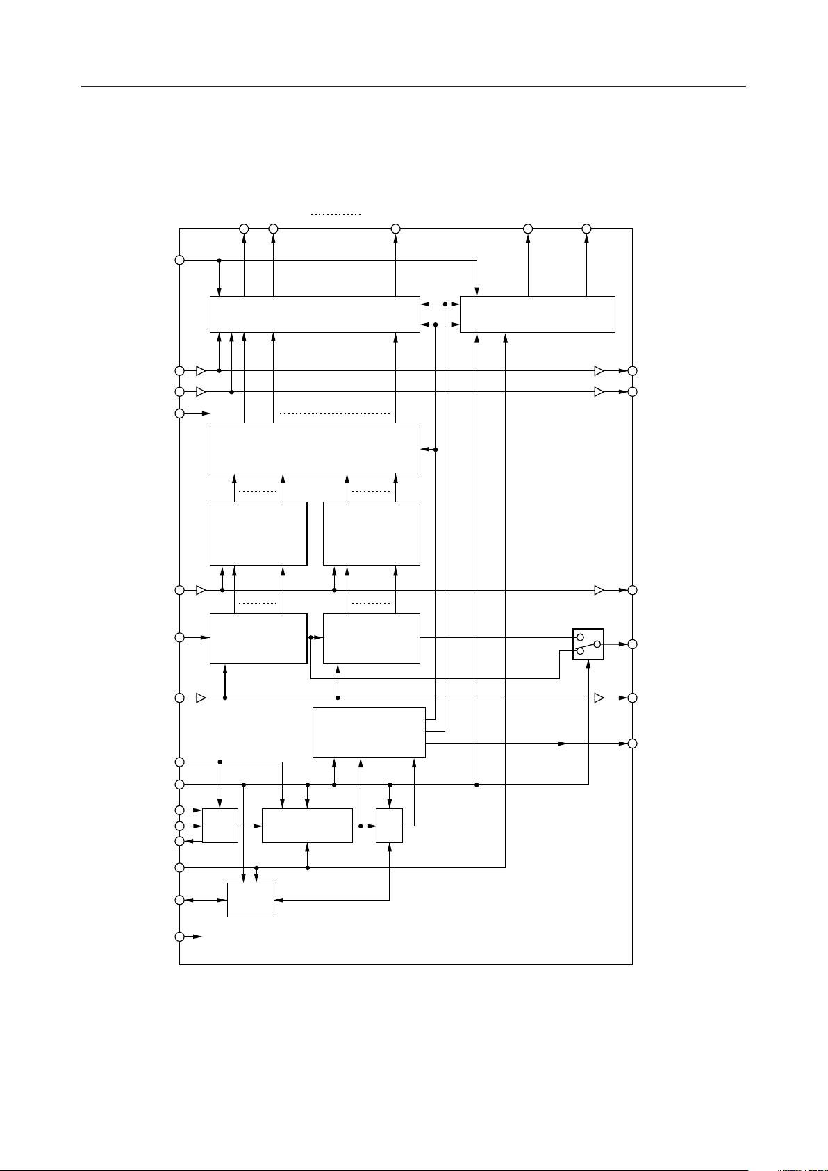
BLOCK DIAGRAM
ML9060¡ Semiconductor
SEG160SEG2SEG1
V
LCD
Segment Drivers
1/2VLCD Generator
& Common Drivers
COM BCOM A
SEG-TEST IN SEG-TEST OUT
BLANK IN BLANK OUT
V
DD
DS0160DS02DS01
Data Selector
DSI160bDSI1bDSI160aDSI1a
L0160aL01a
Data Latch A
LI160aLI1a
Data Latch B
L0160bL01b
LI160bLI1b
LOAD IN LOAD OUT
P0160bP01b
DATA OUT
DATA IN
P0160aP01a
SIa SOa
Shift Register A
SIb SOb
Shift Register B
CLOCK IN CLOCK OUT
Timing Generator
COM OUT
OSC I/E
D/S
OSC1
OSCR
1/64 or 1/128OSC 1/2
OSC2
M/S
SYNC
SYNC
GND
2/17
Page 3
ABSOLUTE MAXIMUM RATINGS
Parameter Symbol Condition Rating Unit
Logic power supply voltage V
LCD Driving voltage V
Input voltage V
Storage temperature T
DD
LCD
I
STG
Ta = 25°C
Ta = 25°C
Ta = 25°C
— –55 to +150 °C
–0.3 to +6.5
0 to 18
GND–0.3 to VDD+0.3
RECOMMENDED OPERATING CONDITIONS
Parameter Symbol Condition Range Unit
Logic power supply voltage VDD* 2.7 to 5.5
LCD Driving voltage V
Operating temperature T
* 4.5 to 16
LCD
op
—
—
— –40 to +85 °C
ML9060¡ Semiconductor
V
V
V
V
V
*: Use with V
DD
≤ V
LCD
Note: Never place a short between an output pin and another output pin or between an output
pin and other pins (input pins, I/O pins, or power supply pins).
3/17
Page 4
ELECTRICAL CHARACTERISTICS
DC Characteristics
Parameter Symbol Condition Min. Typ. Max. Unit Applicable pin
V
*1 0.7V
IH1
"H" Input voltage
"L" Input voltage
Input leakage current 1 I
Input leakage current 2 I
Segment
Common
"H" Output
voltage
Logic
*2
V
IH2
V
*1
IL1
*2 GND — 0.2V
V
IL2
VI = VDD or 0V
L1
VI = VDD or 0V
D/S = "H"
L2
M/S = "L"
V
OHSIO
*3 IO = –150mAV
V
OHC
V
OHL1IO
= –30mAV
= –100mA 0.9V
—
—
(VDD = 2.7 to 5.5V, V
—V
—V
0.8V
DD
DD
GND — 0.3V
= 4.5 to 16V, Ta = –40 to +85°C)
LCD
DD
DD
DD
DD
DATA IN
CLOCK IN
V
LOAD IN
SEG-TEST IN
V
BLANK IN
M/S, D/S
——±1.0
±10
–0.2 — — V SEG1 to SEG160
LCD
–0.2 — — V COM A, COM B
LCD
m
A
OSC1, OSC I/E
m
A SYNC——
DATA OUT
CLOCK OUT
LOAD OUT
SEG-TEST OUT
DD
——
V
BLANK OUT
COM OUT
SYNC
ML9060¡ Semiconductor
"M" Output
voltage
Common
Segment
Common
"L" Output
voltage
Output
resistance
Logic
Segment
Common
"M": Middle level
V
OHL2IO
*3 I
V
OMC
V
OLS
V
*3 IO = 150mA — — 0.2 V
OLC
V
OLL1IO
V
OLL2IO
R
SEG
R
COM
= –200mA 0.9V
= ±150
m
O
A
1/2V
–0.15
DD
LCD
IO = 30mA — — 0.2 V
= 100mA — — 0.1V
= 200mA — — 0.1V
— — 10 kW SEG1 to SEG160
— — 1.5 kW COM A, COM B
— — V OSC2
1/2V
1/2V
LCD
+0.15
LCD
DD
DD
V COM A, COM B
SEG1 to SEG160
COM A, COM B
DATA OUT
CLOCK OUT
LOAD OUT
SEG-TEST OUT
V
BLANK OUT
COM OUT
SYNC
V OSC2
4/17
Page 5
ML9060¡ Semiconductor
Parameter Symbol Condition Min. Typ. Max. Unit
Static supply current *4
Dynamic supply current *4
I
DDS1
I
DDS2
I
LCDS1
I
LCDS2
I
DD1
I
DD2
I
LCD1
I
LCD2
D/S = "L" (Static)
Fix other input levels
at either "H" or "L"
Oscillator stopped
No load
D/S = "H" (1/2duty)
Fix other input levels
at either "H" or "L"
Oscillator stopped
No load
D/S = "L" (Static)
Fix other input levels
at either "H" or "L"
Oscillator stopped
No load
D/S = "H" (1/2duty)
Fix other input levels
at either "H" or "L"
Oscillator stopped
No load
= 5.5V
V
DD
D/S = "L" (Static)
OSC1 is Open
OSC2 is connected to OSCR
Other inputs are "H" or "L"
No load
= 5.5V
V
DD
D/S = "H" (1/2duty)
OSC1 is Open
OSC2 is connected to OSCR
Other inputs are "H" or "L"
No load
= 5.5V
V
DD
D/S = "L" (Static)
OSC1 is Open
OSC2 is connected to OSCR
Other inputs are "H" or "L"
No load
V
= 5.5V
DD
D/S = "H" (1/2duty)
OSC1 is Open
OSC2 is connected to OSCR
Other inputs are "H" or "L"
No load
——
——
——
——
——
——
——
——
TBD
TBD
TBD
TBD
TBD
TBD
TBD
TBD
Applicable
m
A
m
A
m
A
m
A
mA
mA
m
A
m
A
pin
V
DD
V
DD
V
LCD
V
LCD
V
DD
V
DD
V
LCD
V
LCD
*1: Applicable to the DATA IN, LOAD IN, SEG-TEST IN, M/S, D/S, and OSC I/E pins.
*2: Applicable to the CLOCK IN, OSC1, and BLANK IN pins.
*3: Applicable to the voltage drop when the current flows into or out of one COM pin.
*4: The power supply current consumption will be determined finally at the end of sample
evaluations.
The LCD display data of “0” and “1” are input alternately.
5/17
Page 6
Switching Characteristics
Parameter
OSC IN Clock frequency
(external input)
Clock pulse width
(external input)
External Rf clock
frequency
(internal oscillations)
Internal Rf clock frequency
(with the built-in oscillator)
Data clock pulse width
Symbol
f
CP1
t
WCP1
f
OSC1
f
OSC2
f
CP2
t
WCP2
(VDD = 2.7 to 5.5V, V
Condition Min. Typ. Max. Unit Applicable pin
The clock is input to the
OSC1 pin. The pins OSC2
and OSCR are left open.
OSC I/E = "L"
An Rf of 120k W ±2% is
connected between OSC1
and OSC2. OSCR is left
open. OSC I/E = 'H"
OSC1 open. OSC2 and
OSCR shorted. OSC I/E
tied to V
or any "H" level.
DD
= 4.5 to 16V, Ta = –40 to +85°C)
LCD
— — 25.6 kHz
50——µs
7.7 12.8 20.5 kHz
OSC1
OSC1
OSC1, OSC2
OSC1, OSCR,
7.7 12.8 20.5 kHz
OSC2
— — 1 MHzData clock frequency CLOCK IN
100 — — ns
CLOCK IN
ML9060¡ Semiconductor
Data setup time
CLOCK to LOAD
Period
LOAD to CLOCK
Period
CLOCK IN to
DATA OUT delay time
COM OUT to SYNC
delay time
Input signal rise time
Input signal fall time
t
t
t
t
t
WLD
t
PLH
t
PHL
t
DIO
t
DCS
SU
HD
CL
LC
t
t
R
F
CL=15pF
CL=15pF
50——ns
DATA IN
50——nsData hold time CLOCK IN
100 — — ns
100 — — ns
CLOCK IN
LOAD IN
100 — — nsLOAD Pulse width LOAD IN
CLOCK IN
——50ns
DATA OUT
CLOCK IN/OUT
LOAD IN/OUT
——20nsIN to OUT delay time No load
SEG-TEST IN/OUT
BLANK IN/OUT
COM OUT
——40ns
——50ns
——50ns
SYNC
All inputs other than
the OSCR input
* : The specifications of the internal Rf clock frequency and the external Rf clock frequency will
be determined finally at the end of sample evaluations.
6/17
Page 7

TIMING DIAGRAM
t
WCP1
1/f
CP1
t
WCP1
ML9060¡ Semiconductor
OSC1
(External clock)
DATA IN
CLOCK IN
LOAD IN
DATA OUT
V
IH
V
IH
V
IL
t
SU
t
WCP2
V
V
IL
1/f
IL
CP2
V
IH
V
IL
V
IH
V
IL
t
HD
t
WCP2
V
IH
V
IH
V
IL
t
CL
t
t
PLH
PHL
V
VIHV
V
IL
V
IH
IL
V
IL
t
WLD
IH
V
IL
V
OH
V
OL
t
LC
CLOCK IN
LOAD IN
SEG-TEST IN
BLANK IN
CLOCK OUT
LOAD OUT
SEG-TEST OUT
BLANK OUT
All input signals
COM OUT
SYNC
V
IH
V
IL
t
DIO
V
OH
t
R
V
IH
V
IL
1/2V
DD
t
DCS
1/2V
t
DIO
V
OL
t
F
V
IH
V
IL
1/2V
DD
t
DCS
DD
1/2V
DD
7/17
Page 8

ML9060¡ Semiconductor
FUNCTIONAL DESCRIPTION
The ML9060 is an LCD driver LSI with an internal shift register and a set of internal data latches
and is capable of driving LCD displays of up to 320 segments either in the static mode or in the
1/2 duty mode. The display data is read into the shift register serially from the DATA IN pin
at the rising edge of the CLOCK IN input signal. The display data is transferred internally to
the data latches at the High level of the LOAD IN input signal and is output to the segments
via the segment drivers in this IC. The display data in the shift register is output via the DATA
OUT pin in synchronization with the falling edge of the CLOCK IN input signal. The display
data should be input in the sequence of SEG160, SEG159, ... , SEG2, SEG1 for proper display of
data.
Description of Pin Functions
• M/S
This is the input pin for selecting either the Master mode or the Slave mode. This LSI goes into
the master mode when this pin is High and enters the Slave mode when this pin is Low.
• D/S
This input pin is for selecting either the dynamic display mode at 1/2 duty (D mode - “H” input)
or the static display mode (S mode - “L” input).
Note that the internal bias resistor is made ON in the dynamic (D) mode and is turned OFF in
the static mode (S).
• OSC I/E
This is the input pin for selecting whether to use the external clock input mode, or the internal
Rf oscillation mode or the external Rf oscillation mode.
When this pin is tied to the “H” level, the internal Rf oscillation mode or the external Rf
oscillation is used. When this pin is tied to the “L” level, the external clock input is used for the
operation of the LSI.
In the slave mode of operation of this LSI, any input to this pin will be ignored. Hence, tie this
pin to VDD or GND in the slave mode.
• OSC1, OSCR, OSC2
These are the pins for the oscillator for generating the common signal.
In the Master mode (M/S pin = “H”):
It is possible to select from among the three modes - internal Rf oscillation mode, external Rf
oscillation mode, and the external clock input mode. During the static display operation mode,
a common signal with 1/128th the frequency of the clock oscillator is output via the COM OUT
pin.
During the 1/2 duty dynamic display operation mode, a common signal with 1/64th the
frequency of the clock oscillator is output via the COM OUT pin.
• Internal Rf oscillation mode: Tie the OSC I/E pin to “H”, short the pins OSCR and OSC2, and
leave the pin OSC1 open.
• External Rf oscillation mode: Tie the OSC I/E pin to “L”, connect an external resistor Rf
between the pins OSC1 and OSC2, and leave the pin OSCR open.
• External clock input mode: Tie the OSC I/E pin to “L”, leave open the pins OSCR and OSC2,
and input the external clock signal to the pin OSC1.
8/17
Page 9

ML9060¡ Semiconductor
In the Slave mode (M/S pin = “L”):
Leave open the pins OSCR and OSC2 and connect the pin OSC1 to the COM OUT pin of the
ML9060 which has been set in the master mode. The common signal that is input to the pin OSC1
will be used as the internal common signal and is also output via a buffer from the COM OUT
pin.
• COM OUT
This is the common signal output pin. Connect this pin to the OSC1 pin of the ML9060 that is
set in the slave mode.
During operation in the master mode (M/S pin = “H”) for static display, a common signal with
1/128th the frequency of the oscillator is output.
During operation in the master mode (M/S pin = “H”) for 1/2 duty dynamic display, a common
signal with 1/64th the frequency of the oscillator is output.
During operation in the slave mode (M/S pin = “L”), the common signal that is input at the pin
OSC1 is output from this pin via a buffer.
• SYNC
This is the I/O pin for common signal synchronization.
This pin becomes the synchronization signal output pin during operation in the master mode
(M/S pin = “H”) for 1/2 duty dynamic display.
This pin becomes the synchronization signal input pin during operation in the slave mode (M/
S pin = “H”) for 1/2 duty dynamic display.
For cascade operation in the 1/2 duty display mode, connect the SYNC pins of all ML9060 ICs
used together.
During operation in the static display mode, this pin is tied to the “L” level inside the IC.
Connect this pin either to GND or leave it open.
• DATA IN
This is the display data input pin. Input the display data in the sequence of SEG160, SEG159,
... , SEG2, SEG1. The segment is turned ON when the display data is “H” and OFF when “L”.
• DATA OUT
This is the display data output pin. During the static display mode of operation, the data of the
160th stage of the shift register is output from this pin. During the 1/2 duty dynamic display
mode, the data of the 320th stage of the shift register is output from this pin.
• CLOCK IN
This is the input pin for the shift clock of the display data. The display data that is input at the
DATA IN pin is input serially to the shift register at the rising edge of the CLOCK IN signal.
Also, the display data in the shift register is output from the DATA OUT pin at the falling edge
of the CLOCK IN signal.
• CLOCK OUT
This is the output pin for the shift clock of the display data. The shift clock signal that is input
to the CLOCK IN pin is output via a buffer from this pin.
• LOAD IN
This is the input pin for the display data load signal.
The display data in the shift register is output as such to the segment driver when this signal is
at the “H” level. When this signal is made “L”, the shift register is isolated from the segment
drivers, and the display data of the shift register just before this pin goes “L” is retained in the
data latches and transfered to the segment drivers.
9/17
Page 10

ML9060¡ Semiconductor
• LOAD OUT
This is the output pin for the display data load signal. The load signal that is input to the LOAD
IN pin is output from this pin via a buffer.
• SEG-TEST IN
This is the input pin for making all segments ON. When this pin is “H”, all segment outputs
(SEG1 to SEG160) become ON irrespective of the display data and the Blank signal. When this
pin is made “L”, each of the segment outputs (SEG1 to SEG160) become ON or OFF according
to the display data.
• SEG-TEST OUT
This is the output pin for making all segments ON. The segment ON signal that is input to at
the SEG-TEST IN pin is output via a buffer.
• BLANK IN
This is the input pin for making all segments OFF. When this pin is “H”, all segment outputs
(SEG1 to SEG160) become OFF irrespective of the display data. When this pin is made “L”, each
of the segment outputs (SEG1 to SEG160) becomes ON or OFF according to the display data. The
BLANK IN is valid when the segment ON signal is "L".
• BLANK OUT
This is the output pin for making all segments OFF. The segment OFF signal that is input to the
BLANK IN pin is output via a buffer.
• SEG1 to SEG160
These are the signal outputs for driving the LCD segments and are connected to the corresponding
segment pins of the LCD panel.
During the Static mode of operation:
The SEGn output corresponds to bit n of the display data in the data latch A. The display data
in the data latch B becomes invalid. In the segment ON condition, a signal with a phase opposite
to that of the COM OUT signal is output from these pins. In the segment OFF condition, a signal
with a phase identical to that of the COM OUT signal is output from these pins.
During the 1/2 duty dynamic display mode of operation:
The SEGn output corresponds to bit n of the display data in the data latch A when COM A has
been selected and to bin n of the display data in the data latch B when COM B has been selected.
In the segment display ON condition, a signal opposite in phase to that of the selected COM
output is output from these pins. In the segment display OFF condition, a signal identical in
phase to that of the selected COM output is output from these pins.
• COM A, COM B
These are the outputs for LCD display and are connected to the common pins of the LCD panel.
During the Static mode of operation:
COM A and COM B both output a signal with the same phase as that of the COM OUT signal.
10/17
Page 11

ML9060¡ Semiconductor
During the 1/2 duty dynamic display mode of operation:
COM A and COM B change their states at every cycle of the COM OUT signal and repeat the
selected and non-selected modes always opposing each other in phase. A signal with the same
phase as that of the COM OUT signal is output in the selected mode. A voltage equal to 1/2V
LCD
is output in the non-selected mode.
When COM A is in the selected mode (that is, COM B is in the non-selected mode), the segment
outputs (SEG1 to SEG160) output signals corresponding to the display data in the data latch A.
When COM B is in the selected mode (that is, COM A is in the non-selected mode), the segment
outputs (SEG1 to SEG160) output signals corresponding to the display data in the data latch B.
• V
DD
This is the power supply input pin for the logic circuits.
• V
LCD
This is the power supply input pin for the LCD drivers.
• GND
This is the ground pin for all circuits.
11/17
Page 12

Segment Output and Common Output Waveforms
During the 1/2 duty display operation mode:
COM OUT
SYNC
COM A
Selected
COM A
COM B
COM B
Selected
COM A
Selected
COM B
Selected
V
DD
GND
V
DD
GND
V
LCD
1/2V
GND
V
LCD
1/2V
GND
V
LCD
ML9060¡ Semiconductor
LCD
LCD
OFF OFF OFF OFF
SEGn
OFF ON OFF ON
ON OFF ON OFF
ON ON ON ON
Data latch A Data latch B Data latch A Data latch B
During the static display operation mode:
COM OUT
COM A
COM B
GND
V
LCD
GND
V
LCD
GND
V
LCD
GND
V
DD
GND
V
LCD
GND
V
LCD
GND
V
LCD
SEGn
OFF OFF OFF OFF
ON ON ON ON
GND
V
LCD
GND
12/17
Page 13

ML9060¡ Semiconductor
APPLICATION CIRCUIT EXAMPLES
When a single ML9060 is used - Static display mode (internal Rf oscillation mode)
From the controller
LCD Panel 160 segments,
static display
SEG160SEG1
SEG-TEST IN
BLANK IN
LOAD IN
DATA IN
CLOCK IN
D/S M/S OSC1 OSC2 OSCR OSC I/E
ML9060
open
COM
COM A
SYNC
openCOM B
GND
or
open
V
DD
When a single ML9060 is used - 1/2 duty dynamic display mode (external Rf oscillation
mode)
COM A
COM B
SEG160SEG1
COM A
COM B
SYNC
open
V
DD
From the controller
LCD Panel 320 segments,
1/2 Duty dynamic display
SEG-TEST IN
BLANK IN
LOAD IN
DATA IN
CLOCK IN
D/S M/S OSC1 OSC2 OSCR OSC I/E
ML9060
Rf
open
13/17
Page 14

Cascade Connection - Static display mode (external clock input mode)
LCD Panel (160 x n segments)
COM Static
ML9060¡ Semiconductor
From the controller
V
DD
External clock
160
COM A COM A
COM B COM B
SEG-TEST IN
BLANK IN
LOAD IN
DATA IN
CLOCK IN
D/S M/S OSC1 OSC2 OSCR OSC I/E
ML9060
SEG-TEST OUT
BLANK OUT
LOAD OUT
DATA OUT
CLOCK OUT
COM OUT
SYNC
open open
SEG-TEST IN
BLANK IN
LOAD IN
DATA IN
CLOCK IN
D/S M/S OSC1 OSC2 OSCR OSC I/E
160
ML9060
open open
SEG-TEST OUT
BLANK OUT
LOAD OUT
DATA OUT
CLOCK OUT
COM OUT
SYNC
V
DD
or
GND
open
openopen
open
Note: Take care about the resistance and capacitance of wiring for cascade connection.
Cascade Connection - 1/2 duty dynamic display mode (internal Rf oscillation mode)
LCD Panel (320 x n segments)
From the controller
V
DD
160
COM A COM A
COM B COM B
SEG-TEST IN
BLANK IN
LOAD IN
DATA IN
CLOCK IN
D/S M/S OSC1 OSC2 OSCR OSC I/E
ML9060
open
SEG-TEST OUT
BLANK OUT
LOAD OUT
DATA OUT
CLOCK OUT
COM OUT
SYNC
COM A
COM B 1/2 duty dynamic display
160
SEG-TEST IN
BLANK IN
LOAD IN
DATA IN
CLOCK IN
D/S M/S OSC1 OSC2 OSCR OSC I/E
ML9060
SEG-TEST OUT
BLANK OUT
CLOCK OUT
open open
LOAD OUT
DATA OUT
COM OUT
SYNC
V
DD
or
GND
Note: Take care about the resistance and capacitance of wiring for cascade connection.
open
open
open
14/17
Page 15
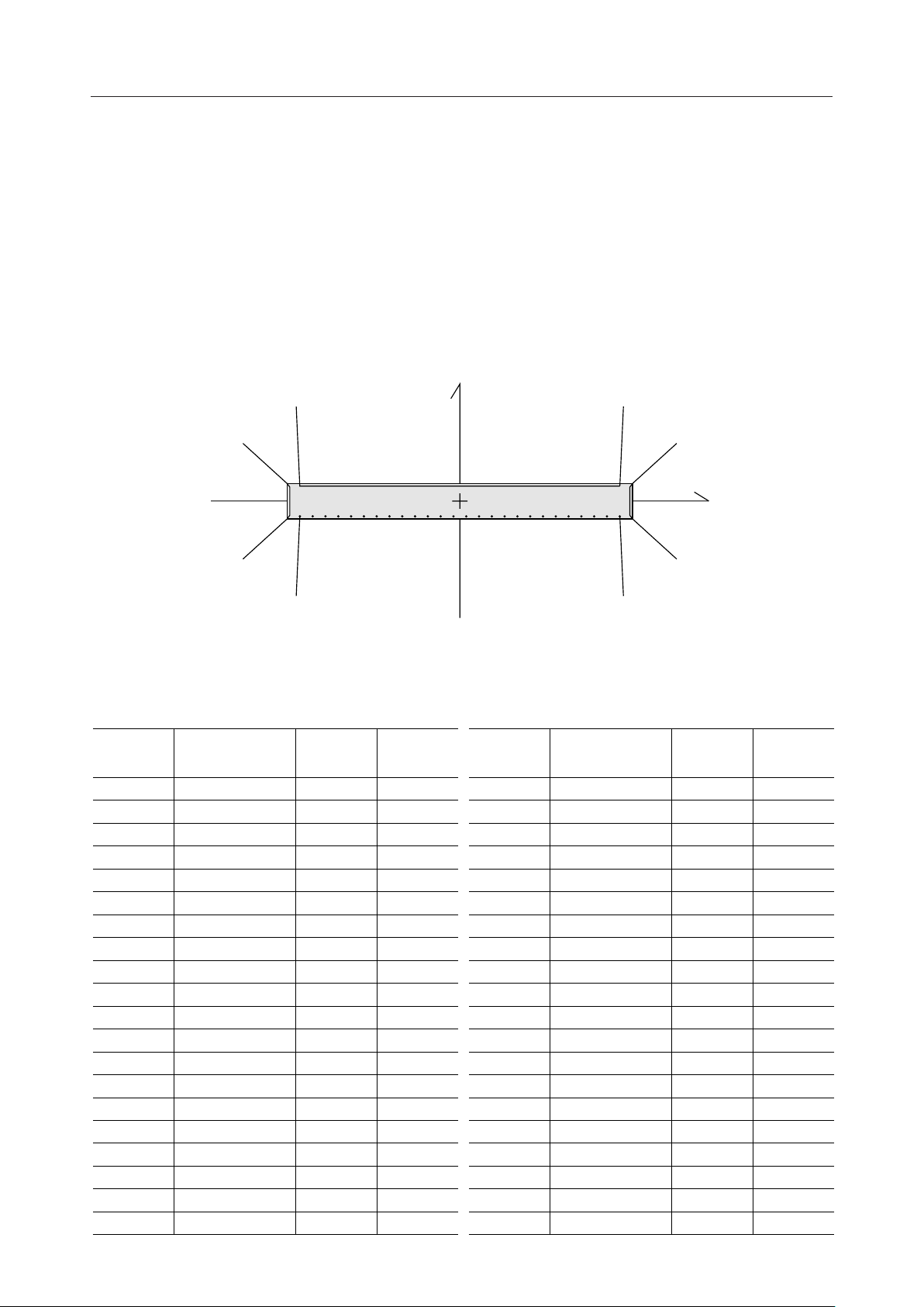
PAD CONFIGURATION
Pad layout (Pattern side)
Chip size : 14.50 ¥ 1.48mm
Chip thickness : 625mm ± 30mm
Minimum bump pitch : 80mm
Bump size : 50 ¥ 80µm
Bump height : 15mm ± 5µm
Bump height inside the chip: max. – min. ≤ 4µm
Bump hardness : max. 100 (HV: 25 g LOAD)
Y
204 37
205 36
ML9060¡ Semiconductor
X
214 27
126
* : The substrate of the chip should either be connected to the GND level or be left open.
Pad Coordinates
267
802
Y-coordinate
(mm)
Pad No.
Pad name
X-coordinate
21 –5614008OSC2
–561 4542
–561 5077
–561 5611
–561 6146
–561 6680
–561 7121
–561 7121
–561 7121
–561 7121
–561 7121
–561 7121
–561 7121
–561 7121
–561 7121
–561 7121
–561 6680
–561 6600
–561 6520
–561 6440
22 OSCR
23 OSC1
24
25
26
NC
NC
NC
27
28
29
30
31
32
33
34
35
36
NC
DATA IN
NC
CLOCK IN
LOAD IN
SEG-TEST IN
BLANK IN
NC
NC
37 NC
38 NC
39 NC
40 COMA
(mm)
Y-coordinate
(mm)
–561
–561
–561
–561
–561
–360NC
–280
–200
–120
Pad No.
1 –561–6680NC
2
3
4
5
6
7
8
9
10
11
12
13
14
15
16
17
18
19
20
Pad name
NC
SYNC
NC
COMOUT
NC
V
LCD
V
LCD
V
LCD
NC
GND
GND
GND
D/S
OSC I/E
M/S
V
DD
V
DD
V
DD
NC
X-coordinate
(mm)
–6146
–5611
–5077
–4542
–4008
–3474
–2939
–2405
–1870
–1336
–802
–267
1336
1870
2405
2939
3474
–40
40
120
200
280
360
561
561
561
561
NC: No Connection
15/17
Page 16

ML9060¡ Semiconductor
Pad No.
Pad name
41 5616360COM B
42
43
44
45
46
47
48
49
50
51
52
53
54
55
56
57
58
59
60
61
62
63
64
65
66
67
68
69
70
71
72
73
74
75
76
77
78
79
80
81
82
83
84
85
X-coordinate
(mm)
6280
6200
6120
6040
5960
5880
5800
5720
5640
5560
5480
5400
5320
5240
5160
5080
5000
4920
4840
4760
4680
4600
4520
4440
4280
4200
4120
4040
3960
3880
3800
3720
3640
3560
3480
3400
3320
3240
3080
3000
2920
2840
Y-coordinate
(mm)
Pad No.
86 5612760SEG45
561SEG1 561SEG46
561SEG2 561SEG47
561SEG3 561SEG48
561SEG4 561SEG49
561SEG5 561SEG50
561SEG6 561SEG51
561SEG7 561SEG52
561SEG8 561SEG53
561SEG9 561SEG54
561SEG10 561SEG55
561SEG11 561SEG56
561SEG12 561SEG57
561SEG13 561SEG58
561SEG14 561SEG59
561SEG15 561SEG60
561SEG16 561SEG61
561SEG17 561SEG62
561SEG18 561SEG63
561SEG19 561SEG64
561SEG20 561SEG65
561SEG21 561SEG66
561SEG22 561SEG67
561SEG23 561SEG68
561SEG24 561SEG69
87
88
89
90
91
92
93
94
95
96
97
98
99
100
101
102
103
104
105
106
107
108
109
110
1114360 760561SEG25 561SEG70
561SEG26 561SEG71
561SEG27 561SEG72
561SEG28 561SEG73
561SEG29 561SEG74
561SEG30 561SEG75
561SEG31 561SEG76
561SEG32 561SEG77
561SEG33 561SEG78
561SEG34 561SEG79
561SEG35 561SEG80
561SEG36 561SEG81
561SEG37 561SEG82
561SEG38 561SEG83
561SEG39 561SEG84
561SEG40 561SEG85
561SEG41 561SEG86
561SEG42 561SEG87
561SEG43 561SEG88
561SEG44 561SEG89
112
113
114
115
116
117
118
119
120
121
122
123
124
125
1263160
127
128
129
130
Pad name
X-coordinate
(mm)
2680
2600
2520
2440
2360
2280
2200
2120
2040
1960
1880
1800
1720
1640
1560
1480
1400
1320
1240
1160
1080
1000
920
840
680
600
520
440
360
280
200
120
40
–40
–120
–200
–280
–360
–440
–520
–600
–680
–760
Y-coordinate
(mm)
16/17
Page 17

ML9060¡ Semiconductor
Pad No.
Pad name
131 561–840SEG90
132
133
134
135
136
137
138
139
140
141
142
143
144
145
146
147
148
149
150
151
152
153
154
155
156
157
158
159
160
161
162
163
164
165
166
167
168
169
170
171
172
173
174
175
X-coordinate
(mm)
–920
–1000
–1080
–1160
–1240
–1320
–1400
–1480
–1560
–1640
–1720
–1800
–1880
–1960
–2040
–2120
–2200
–2280
–2360
–2440
–2520
–2600
–2680
–2760
–2920
–3000
–3080
–3160
–3240
–3320
–3400
–3480
–3560
–3640
–3720
–3800
–3880
–3960
–4040
–4120
–4200
–4280
–4360
Y-coordinate
(mm)
Pad No.
Pad name
176 561–4440SEG135
561SEG91 561SEG136
561SEG92 561SEG137
561SEG93 561SEG138
561SEG94 561SEG139
561SEG95 561SEG140
561SEG96 561SEG141
561SEG97 561SEG142
561SEG98 561SEG143
561SEG99 561SEG144
561SEG100 561SEG145
561SEG101 561SEG146
561SEG102 561SEG147
561SEG103 561SEG148
561SEG104 561SEG149
561SEG105 561SEG150
561SEG106 561SEG151
561SEG107 561SEG152
561SEG108 561SEG153
561SEG109 561SEG154
561SEG110 561SEG155
561SEG111 561SEG156
561SEG112 561SEG157
561SEG113 561SEG158
561SEG114 561SEG159
177
178
179
180
181
182
183
184
185
186
187
188
189
190
191
192
193
194
195
196
197
198
199
200
201–2840 –6440561SEG115 561SEG160
561SEG116 561NC
561SEG117 561NC
561SEG118 561NC
561SEG119 360NC
561SEG120 280NC
561SEG121 200BLANKOUT
561SEG122 120SEG-TESTOUT
561SEG123 40LOADOUT
561SEG124 –40CLOCKOUT
561SEG125 –120NC
561SEG126 –200DATAOUT
561SEG127 –280NC
561SEG128 –360NC
202
203
204
205
206
207
208
209
210
211
212
213
214
561SEG129
561SEG130
561SEG131
561SEG132
561SEG133
561SEG134
X-coordinate
(mm)
–4520
–4600
–4680
–4760
–4840
–4920
–5000
–5080
–5160
–5240
–5320
–5400
–5480
–5560
–5640
–5720
–5800
–5880
–5960
–6040
–6120
–6200
–6280
–6360
–6520
–6600
–6680
–7121
–7121
–7121
–7121
–7121
–7121
–7121
–7121
–7121
–7121
Y-coordinate
(mm)
17/17
Page 18

E2Y0002-29-11
NOTICE
1. The information contained herein can change without notice owing to product and/or
technical improvements. Before using the product, please make sure that the information
being referred to is up-to-date.
2. The outline of action and examples for application circuits described herein have been
chosen as an explanation for the standard action and performance of the product. When
planning to use the product, please ensure that the external conditions are reflected in the
actual circuit, assembly, and program designs.
3. When designing your product, please use our product below the specified maximum
ratings and within the specified operating ranges including, but not limited to, operating
voltage, power dissipation, and operating temperature.
4. Oki assumes no responsibility or liability whatsoever for any failure or unusual or
unexpected operation resulting from misuse, neglect, improper installation, repair, alteration
or accident, improper handling, or unusual physical or electrical stress including, but not
limited to, exposure to parameters beyond the specified maximum ratings or operation
outside the specified operating range.
5. Neither indemnity against nor license of a third party’s industrial and intellectual property
right, etc. is granted by us in connection with the use of the product and/or the information
and drawings contained herein. No responsibility is assumed by us for any infringement
of a third party’s right which may result from the use thereof.
6. The products listed in this document are intended for use in general electronics equipment
for commercial applications (e.g., office automation, communication equipment,
measurement equipment, consumer electronics, etc.). These products are not authorized
for use in any system or application that requires special or enhanced quality and reliability
characteristics nor in any system or application where the failure of such system or
application may result in the loss or damage of property, or death or injury to humans.
Such applications include, but are not limited to, traffic and automotive equipment, safety
devices, aerospace equipment, nuclear power control, medical equipment, and life-support
systems.
7. Certain products in this document may need government approval before they can be
exported to particular countries. The purchaser assumes the responsibility of determining
the legality of export of these products and will take appropriate and necessary steps at their
own expense for these.
8. No part of the contents cotained herein may be reprinted or reproduced without our prior
permission.
9. MS-DOS is a registered trademark of Microsoft Corporation.
Copyright 1999 Oki Electric Industry Co., Ltd.
Printed in Japan
 Loading...