

Page 1

PEDL9050-02
Preliminary
PEDL9050-02
¡ Semiconductor ML9050/9051
¡ Semiconductor
This version: Dec. 1999
Previous version: Jun. 1999
ML9050/9051
132-Channel LCD Driver with Built-in RAM for LCD Dot Matrix Displays
GENERAL DESCRIPTION
The ML9050/9051 is an LSI for dot matrix graphic LCD devices carrying out bit map display.
This LSI can drive a dot matrix graphic LCD display panel under the control of an 8-bit
microcomputer. Since all the functions necessary for driving a bit map type LCD device are
incorporated in a single chip, using the ML9050/9051 makes it possible to realize a bit map type
dot matrix graphic LCD display system with only a few chips.
Since the bit map method in which one bit of display RAM data turns ON or OFF one dot in the
display panel, it is possible to carry out displays with a high degree of freedom such as Chinese
character displays, etc. With one chip, it is possible to construct a graphic display system with
a maximum of 132 ¥ 65 dots. The display can be expanded further using two chips.
The ML9050/9051 is made using a CMOS process. Because it has a built-in RAM, low power
consumption is one of its features, and is therefore suitable for displays in battery-operated
portable equipment.
The ML9050 has 65 common signal outputs and 132 segment signal outputs and one chip can
drive a display of up to 65 ¥ 132 dots.
The ML9051 has 49 common signal outputs and 132 segment signal outputs and one chip can
drive a display of up to 49 ¥ 132 dots.
This device is not resistant to radiation or to light.
FEATURES
• Direct display of the RAM data using the bit map method
Display RAM data "1" ... Dot is displayed
Display RAM data "0" ... Dot is not displayed
• Display RAM capacity
ML9050/9051: 65 ¥ 132 = 8580 dots
• LCD Drive circuits
ML9050: 65 common outputs, 132 segment outputs
ML9051: 49 common outputs, 132 segment outputs
• Microcomputer interface: Can select an 8-Bit parallel or serial interface
• Built-in voltage multiplier circuit for the LCD drive power supply
• Built-in LCD drive power supply adjustment circuit
• Built-in LCD drive bias resistors
• Line reversal drive/frame reversal drive (selected by a command)
• Built-in oscillator circuit (Internal RC oscillator/external clock input)
• A variety of commands
Read/write of display data, display ON/OFF, normal/reverse display, all dots ON/all dots
OFF, set page address, set display start address, etc.
• Power supply voltage
Logic power supply: VDD-VSS = 1.8 V to 5.5 V
Voltage multiplier reference voltage: VIN-VSS = 1.8 V to V
(5-Times multiplier Æ 1.8 V to 3.6 V, 6-times multiplier Æ 1.8 to 3 V, 7-times multiplier Æ 1.8
to 2.5 V)
LCD Drive voltage: VBI-VSS = 6.0 to 18 V
• Package: Gold bump chip, TCP
DD
1/71
Page 2
PEDL9050-02
¡ Semiconductor ML9050/9051
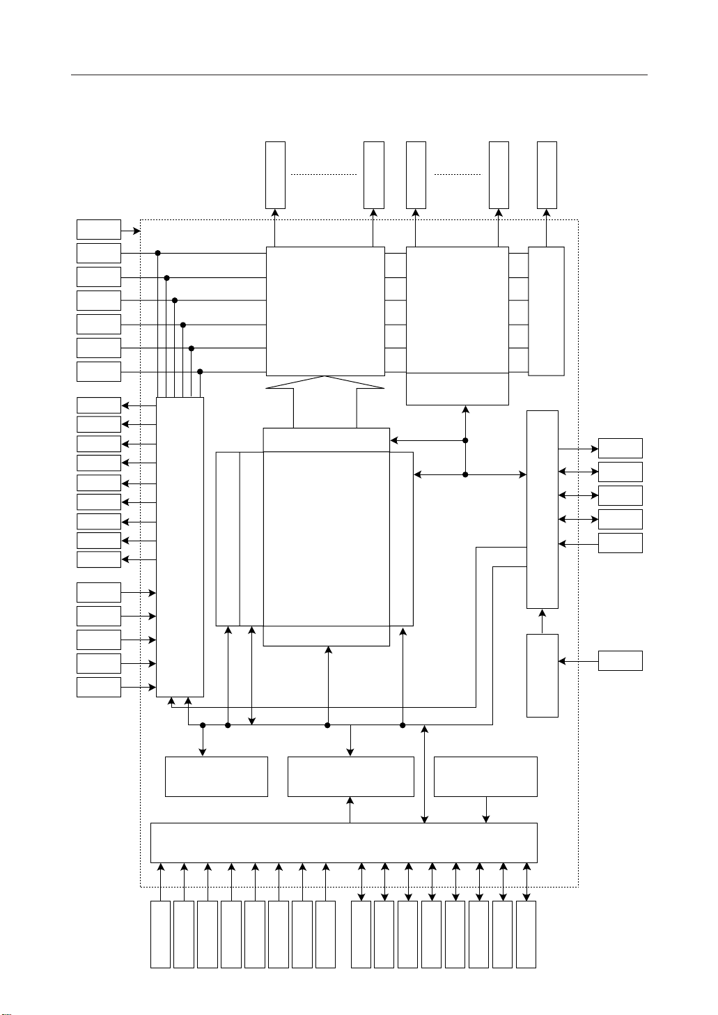
BLOCK DIAGRAM
V
DD
V1
V2
V3
V4
V5
V
SS
VC1+
VS1–
VC2+
VS2–
VC3+
VC4+
VC5+
VC6+
VOUT
V
IN
VR
VRS
IRS
HPM
Display data latch circuit
I/O Buffer
Power supply circuit
Page address circuit
Column address circuit
SEG0
SEG Drivers
Display data RAM
132 ¥ 65
SEG131
COM0
Drivers
COM Output state
selection cricuit
Line address circuit
COM
COM63
COMS
COMS
FRS
FR
CL
DOF
M/S
CLS
Oscillator circuit Display timing generator circuit
C86
Bus holder
CS1
CS2
A0
RD(E)
Command decoder Status
MPU lnterface
D5
P/S
RES
D7(SI)
WR(R/W)
D6(SCL)
D4
D3
D2
D1
D0
2/71
Page 3
PEDL9050-02
¡ Semiconductor ML9050/9051
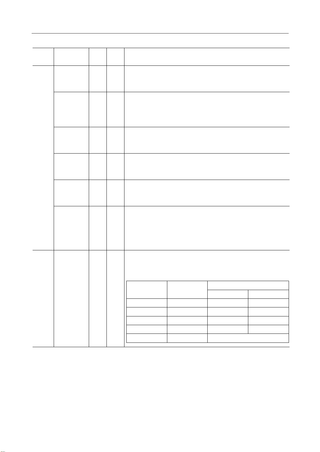
PIN DESCRIPTION
Function
MPU
Interface
Pin name
CS2
(E)
(R/W)
Number
of pins
8
1IA0
1IRES
2ICS1
1IRD
1IWR
1IC86
I/O
This is an 8-bit bi-directional data bus that can be connected to an 8-bit
I/OD0 to D7
or 16-bit standard MPU data bus. When a serial interface is selected (P/S
= "L"):
D7: Serial data input pin (SI)
D6: Serial clock input pin (SCL)
In this case, D0 to D5 will be in the Hi-Z state. D0 to D7 will all be in the
Hi-Z state when the chip select is in the inactive state.
Normally, the lowest bit of the MPU address bus is connected and used
for distinguishing between data and commands.
A0 = "H": Indicates that D0 to D7 is display data.
A1 = "L": Indicates that D0 to D7 is control data.
Initial setting is made by making RES = "L". The reset operation is made
during the active level of the RES signal.
These are the chip select signals. The Chip Select of the LSI becomes
active when CS1 is "L" and also CS2 is "H" and allows the input/output of
data or commands.
The active level of this signal is "L" when connected to an 80-series MPU.
This terminal is connected to the RD signal of the 80-series MPU, and the
data bus of the ML9050/9051 goes into the output state when this signal
is "L".
The active level of this signal is "H" when connected to a 68-series MPU.
This pin will be the Enable and clock input pin when connected to a 68series MPU.
The active level of this signal is "L" when connected to an 80-series MPU.
This terminal is connected to the WR signal of the 80-series MPU. The
data on the data bus is latched into the ML9052 at the rising edge of the
WR signal.
When connected to a 68-series MPU, this pin becomes the input pin for
the Read/Write control signal.
R/W = "H": Read, R/W = "L": Write
This is the pin for selecting the MPU interface type.
C86 = "H": 68-Series MPU interface.
C86 = "L": 80-Series MPU interface.
Description
3/71
Page 4

PEDL9050-02
¡ Semiconductor ML9050/9051
Function
MPU
Interface
Oscillator
circuit
Display
timing
generator
circuit
Pin name
P/S
Number
of pins
I/O
1I
1ICLS
1IM/S
Description
This is the pin for selecting parallel data input or serial data input.
P/S = "H": Parallel data input.
P/S = "L": Serial data input.
The pins of the LSI have the following functions depending on the state of
P/S input.
P/S Data/command Data Read/Write Serial clock
"H"
"L"
A0
A0
D0 to D7
SI (D7)
RD, WR
Write only
SCL (D6)
When P/S is "L", D0 to D5 will go into the Hi-Z state. In this condition,
the data on the lines D0 to D5 can be "H", "L", or open. The pins RD (E)
and WR (R/W) should be tied to either the "H" level or the "L" level.
During serial data input, it is not possible to read the display data in the
RAM.
This is the pin for selecting whether to enable or disable the internal
oscillator circuit for the display clock.
CLS = "H": The internal oscillator circuit is enabled.
CLS = "L": The internal oscillator circuit is disabled (External input).
When CLS = "L", the display clock is input at the pin CL.
This is the pin for selecting whether master operation or slave operation
is made towards the ML9050/9051. During master operation, the
synchronization with the LCD display system is achieved by inputting the
timing signals necessary for LCD display.
M/S = "H": Master operation
M/S = "L": Slave operation
The functions of the different circuits and pins will be as follows
depending on the states of M/S and CLS signals.
Power
supply circuit
Enabled
Enabled
Disabled
Disabled
Output
Input
Input
Input
"L"
"L"
Oscillator
circuit
Enabled
Disabled
Disabled
Disabled
M/S CLS DOFFRSFRCL
"H" "H"
"L" "H"
Output
Output
Input
Input
Output
Output
Output
Output
Output
Output
Input
Input
4/71
Page 5
PEDL9050-02
¡ Semiconductor ML9050/9051
Function
Display
timing
generator
circuit
Power
supply
circuit
Pin name
DD
SS
IN
Number
of pins
1 I/OCL
1 I/OFR
1 I/ODOF
1OFRS
1IIRS
1IHPM
13 —V
9—V
4—V
DescriptionI/O
This is the display clock input/output pin.
The function of this pin will be as follows depending on the states of M/S
and CLS signals.
M/S CLS CL
"H" "H"
"L" "H"
"L"
"L"
Output
Input
Input
Input
When the ML9050/9051 is used in the master/slave mode, the
corresponding CL pin has to be connected.
This is the input/output pin for LCD display frame reversal signal.
M/S = "H": Output
M/S = "L": Input
When the ML9050/9051 is used in the master/slave mode, the
corresponding FR pin has to be connected.
This is the blanking control pin for the LCD display.
M/S = "H": Output
M/S = "L": Input
When the ML9050/9051 is used in the master/slave mode, the
corresponding DOF pin has to be connected.
This is the output pin for static drive.
This pin is used in combination with the FR pin.
This is the pin for selecting the resistor for adjusting the voltage V1.
IRS = "H": The internal resistor is used.
IRS = "L": The internal resistor is not used. The voltage V1 is adjusted
using the external potential divider resistors connected to the pins VR.
This pin is effective only in the master operation. This pin is tied to the
"H" or the "L" level during slave operation.
This is the power control pin for the LCD drive power supply circuit.
HPM = "H": Normal mode
HPM = "L": High power mode
This pin is effective only during master operation mode. This pin is tied to
the "H" or the "L" level during slave operation.
This pin is tied to the MPU power supply terminal VCC.
This is the 0 V pin connected to the system ground (GND).
This is the reference power supply of the voltage multiplier circuit for
driving the LCD.
5/71
Page 6
PEDL9050-02
¡ Semiconductor ML9050/9051
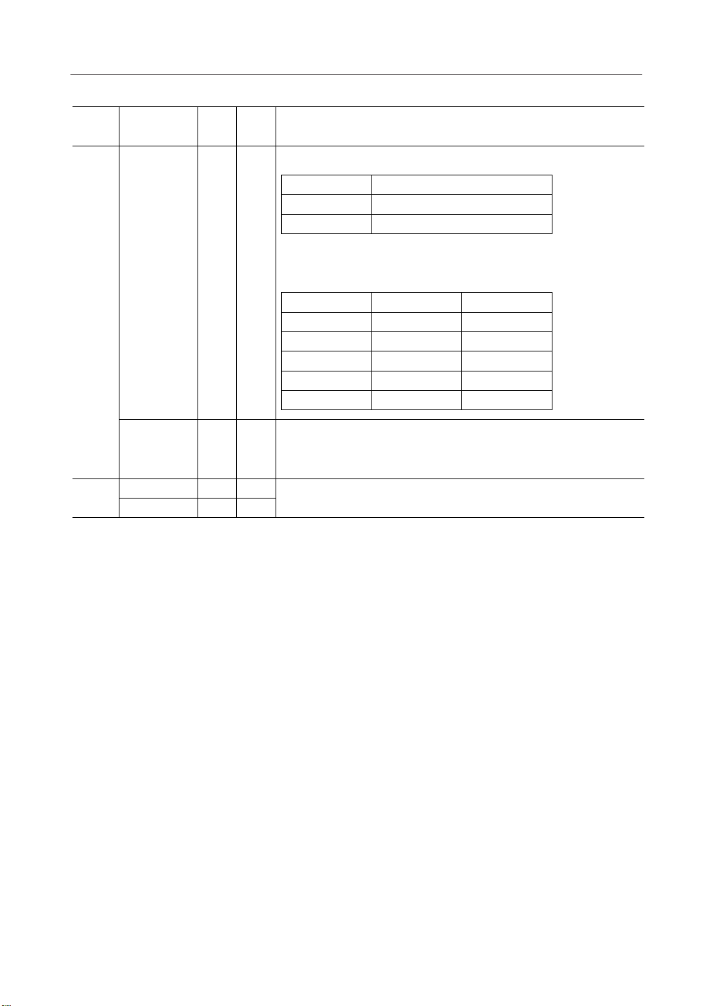
Function
Power
supply
circuit
Pin name
RS
OUT
V2
V3
V4
V5
Number
of pins
2—V
2OV
10 —V1
DescriptionI/O
This is the external input VREG power supply for the LCD power supply
voltage adjustment circuit.
(This pin should be left open when not used as an external input)
This pin is effective only in the case of optional devices with the VREG
external input option.
These are the output pins during voltage multiplication. Connect a
capacitor between these pins and V
.
SS
These are the multiple level power supply pins for the LCD power supply.
The voltages specified for the LCD cells are applied to these pins after
resistor network voltage division or after impedance transformation using
operational amplifiers. The voltages are specified taking V
as the
SS
reference, and the following relationship should be maintained among
them.
V1 ≥ V2 ≥ V3 ≥ V4 ≥ V5 ≥ V
SS
Master operation: When the power supply is ON, the following voltages
are applied to V2 to V5 from the built-in power supply circuit. The
selection of voltages is determined by the LCD bias set command.
ML9050
V2 8/9 ¥ V1 6/7 ¥ V1
V3 7/9 ¥ V1 5/7 ¥ V1
V4 2/9 ¥ V1 2/7 ¥ V1
V5 1/9 ¥ V1 1/7 ¥ V1
ML9051
V2 7/8 ¥ V1 5/6 ¥ V1
V3 6/8 ¥ V1 4/6 ¥ V1
V4 2/8 ¥ V1 2/6 ¥ V1
V5 1/8 ¥ V1 1/6 ¥ V1
2IVR
Voltage adjustment pins. Voltages between V1 and VSS are applied
using a resistance voltage divider.
These pins are effective only when the internal resistors for voltage V1
adjustment are not used (IRS = "L").
Do not use these pins when the internal resistors for voltage V1
adjustment are used (IRS = "H").
2OVC1+
These are the pins for connecting the positive side of the capacitors for
voltage multiplication.
Connect capacitors between VS1– and these pins.
2OVS1–
These are the pins for connecting the negative side of the capacitors for
voltage multiplication.
Connect capacitors between these pins and VC1+, VC3+, and VC5+.
6/71
Page 7
PEDL9050-02
¡ Semiconductor ML9050/9051
Function
Power
supply
circuit
LCD
Drive
output
Pin name
SEG131
Number
of pins
2OVC2+
2OVS2–
2OVC3+
2OVC4+
2OVC5+
2OVC6+
132 OSEG0 to
DescriptionI/O
These are the pins for connecting the positive side of the capacitors for
voltage multiplication.
Connect capacitors between VS2– and these pins.
These are the pins for connecting the negative side of the capacitors for
voltage multiplication.
Connect capacitors between these pins and VC2+, VC4+, and VC6+
(during 7-times voltage multiplication).
These are the pins for connecting the positive side of the capacitors for
voltage multiplication.
Connect capacitors between VS1– and these pins.
These are the pins for connecting the positive side of the capacitors for
voltage multiplication.
Connect capacitors between VS2– and these pins.
These are the pins for connecting the positive side of the capacitors for
voltage multiplication.
Connect capacitors between VS1– and these pins.
These are the pins for connecting the positive side of the capacitors for
voltage multiplication.
Connect capacitors between VS2– and these pins (during 7-times voltage
multiplication).
For 6-times voltage multiplication, connect these pins to the V
OUT
pin.
These are the LCD segment drive outputs.
One of the levels among V1, V3, V4, and V
is selected depending on the
SS
combination of the display RAM content and the FR signal.
RAM Data FR
Normal display Reverse display
Output voltage
H H V1 V3
H L VSS V4
L H V3 V1
L L V4 V
Power save — V
SS
SS
7/71
Page 8
PEDL9050-02
¡ Semiconductor ML9050/9051
Function
Pin name
LCD
Drive
COMn
output
Test pin ITEST0
Number
of pins
96 OCOM0 to
2OCOMS
DescriptionI/O
These are the LCD common drive outputs.
COM
ML9050 COM0 to COM63
ML9051
COM0 to COM47
One of the levels among V1, V2, V5, and VSS is selected depending on
the combination of the scan data and the FR signal.
Scan data FR Output voltage
H H VSS
HLV1
LHV2
LLV5
Power save — V
SS
These are the COM output pins only for indicators. Both pins output the
same signal. Leave these pins open when they are not used.
The same signal is output in both master and slave operation modes.
These are the pins for testing the IC chip. Leave these pins open during
normal use.
OTEST1
8/71
Page 9
PEDL9050-02
¡ Semiconductor ML9050/9051
FUNCTIONAL DESCRIPTION
MPU Interface
• Selection of interface type
The ML9050/9051 carries out data transfer using either the 8-bit bi-directional data bus (D7 to
D0) or the serial data input line (SI). Either the 8-bit parallel data input or serial data input can
be selected as shown in Table 1 by setting the P/S pin to the "H" or the "L" level.
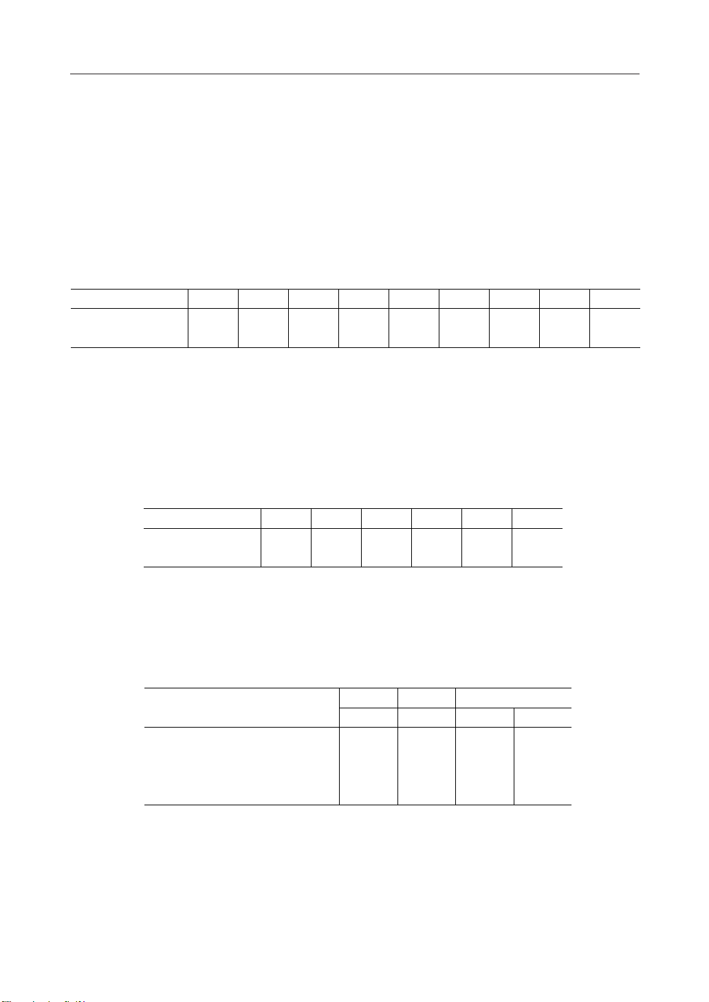
Table 1
P/S CS1 CS2 A0 RD WR C86 D7 D6
H: Parallel input
L: Serial input
CS1
CS1
CS2
CS2
A0
A0
RD
—
WR
—
C86
—
D7
SI
D6
SCL
D5 to D0
D5 to D0
(HZ)
A hyphen (—) indicates that the pin can be tied to the "H" or the "L" level.
• Parallel interface
When the parallel interface is selected, (P/S = "H"), it is possible to connect this LSI directly to the
MPU bus of either an 80-series MPU or a 68-series MPU as shown in Table 2 depending on
whether the pin C86 is set to "H" or "L".
Table 2
P/S CS1 CS2 A0 RD WR
H: 68-Series MPU bus
L: 80-Series MPU bus
CS1
CS1
CS2
CS2
A0
A0
E
RD
D7 to D0
R/WWRD7 to D0
D7 to D0
The data bus signals are identified as shown in Table 3 below depending on the combination of
the signals A0, RD(E), and WR(R/W) of Table 2.
Table 3
Display data read
Display data write
Status read
Control data write (command)
Common 68-Series 80-Series
A0 R/WRD WR
1
1
0
0
1
0
1
0
0
1
0
1
1
0
1
0
9/71
Page 10
PEDL9050-02
¡ Semiconductor ML9050/9051
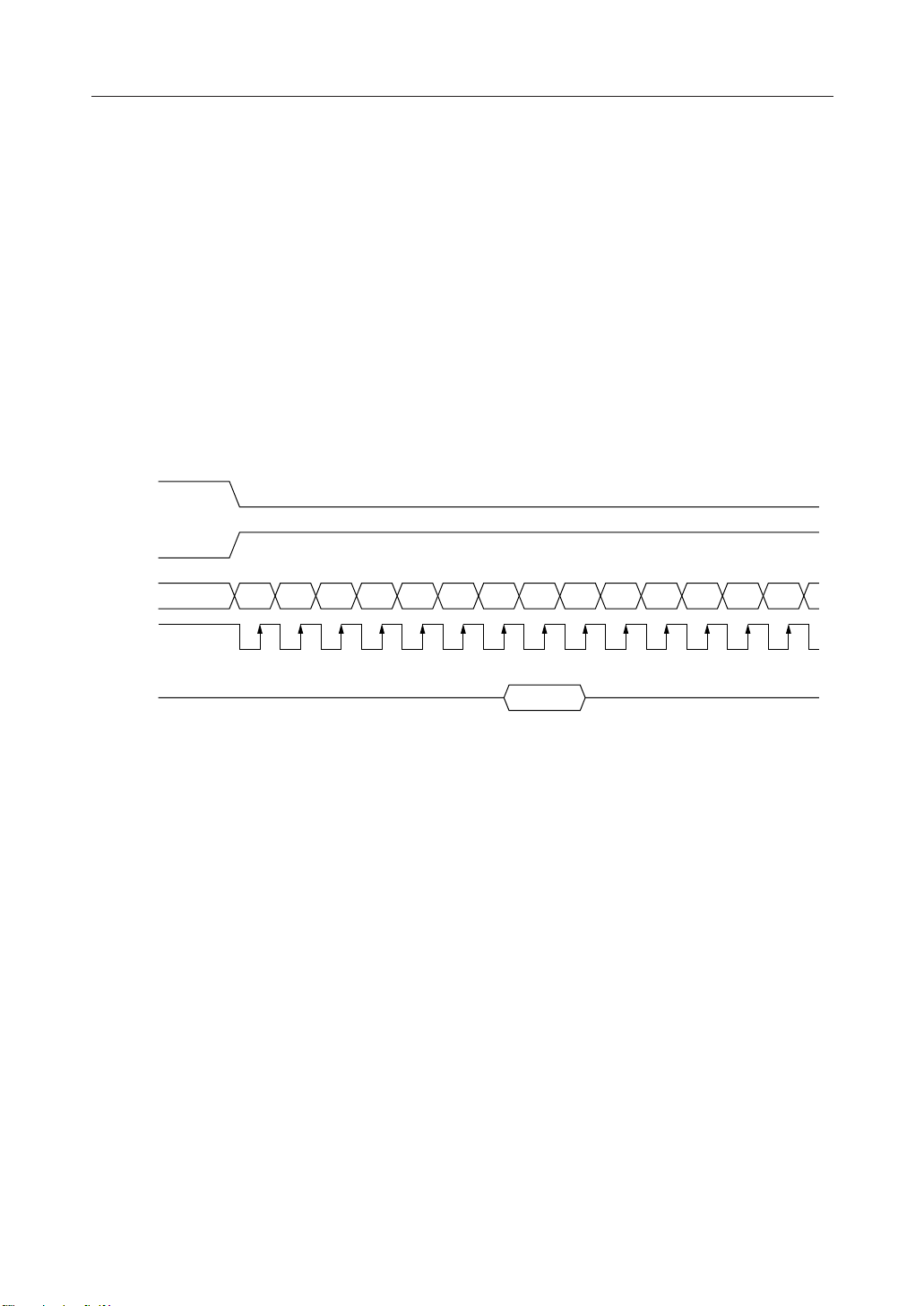
Serial interface
When the serial interface is selected (P/S = "L"), the serial data input (SI) and the serial clock input
(SCL) can be accepted if the chip is in the active state (CS1 = "L" and CS2 = "H"). The serial interface
consists of an 8-bit shift register and a 3-bit counter. The serial data is read in from the serial data
input pin in the sequence D7, D6, ... , D0 at the rising edge of the serial clock input, and is
converted into parallel data at the rising edge of the 8th serial clock pulse and processed further.
The identification of whether the serial data is display data or command is judged based on the
A0 input, and the data is treated as display data when A0 is "H" and as command when A0 is "L".
The A0 input is read in and identified at the rising edge of the (8 ¥ n) th serial clock pulse after
the chip has become active. Fig. 1 shows the signal chart of the serial interface. (When the chip
is not active, the shift register and the counter are reset to their initial states. No data read out
is possible in the case of the serial interface. It is necessary to take sufficient care about wiring
termination reflection and external noise in the case of the SCL signal. We recommend
verification of operation in an actual unit.)
CS1
CS2
D7SI
D62D53D44D35D26D17D08D79D610D511D412D313D2
SC
A0
1
14
Fig. 1
• Chip select
The ML9050/9051 has the two chip select pins CS1 and CS2, and the MPU interface or the serial
interface is enabled only when CS1 = "L" and CS2 = "H". When the chip select signals are in the
inactive state, the D0 to D7 lines will be in the high impedance state and the inputs A0, RD, and
WR will not be effective. When the serial interface has been selected, the shift register and the
counter are reset when the chip select signals are in the inactive state.
• Accessing the display data RAM and the internal registers
Accessing the ML9050/9051 from the MPU side requires merely that the cycle time (t
CYC
) be
satisfied, and high speed data transfer without requiring any wait time is possible. Also, during
the data transfer with the MPU, the ML9050/9051 carries out a type of pipeline processing
between LSIs via a bus holder associated with the internal data bus. For example, when the MPU
writes data in the display data RAM, the data is temporarily stored in the bus holder, and is then
written into the display data RAM before the next data read cycle. Further, when the MPU reads
out data in the display data RAM, first a dummy data read cycle is carried out to temporarily store
the data in the bus holder which is then placed on the system bus and is read out during the next
read cycle. There is a restriction on the read sequence of the display data RAM, which is that the
read instruction immediately after setting the address does not read out the data of that address,
but that data is output as the data of the address specified during the second data read sequence,
and hence care should be taken about this during reading. Therefore, always one dummy read
is necessary immediately after setting the address or after a write cycle. This relationship is
shown in Figs 2(a) and 2(b).
10/71
Page 11
PEDL9050-02
¡ Semiconductor ML9050/9051
• Data write
WR
MPU
DATA
BUS Holder
Write Signal
Internal timing
N
Latch
N N+1 N+2 N+3
N+1 N+2 N+3
Fig. 2(a)
• Data read
WR
RD
MPU
DATA
Address
Preset
Read Signal
Column
Address
Internal timing
BUS Holder
N
Address Set
#n
N n n+1
Preset N
N n n+1 n+2
Dummy
Read
Increment N+1 N+2
Data Read
#n
Data Read
#n+1
Fig. 2(b)
• Busy flag
The busy flag being "1" indicates that the ML9050/9051 is carrying out internal operations, and
hence no instruction other than a status read instruction is accepted during this period. The busy
flag is output at pin D7 when a status read instruction is executed. If the cycle time (t
CYC
) is
established, there is no need to check this flag before issuing every command and hence the
processing performance of the MPU can be increased greatly.
11/71
Page 12

PEDL9050-02
¡ Semiconductor ML9050/9051
Display data RAM
• Display data RAM
This is the RAM storing the dot data for display and has an organization of 65 (8 pages ¥ 8 bits
+1) ¥ 132 bits. It is possible to access any required bit by specifying the page address and the
column address. Since the display data D7 to D0 from the MPU corresponds to the LCD display
in the direction of the common lines as shown in Fig. 3, there are fewer restrictions during display
data transfer when the ML9050/9051 is used in a multiple chip configuration, thereby making
it easily possible to realize a display with a high degree of freedom. Also, since the display data
RAM read/write from the MPU side is carried out via an I/O buffer, it is done independent of
the signal read operation for the LCD drive. Consequently, the display is not affected by
flickering, etc., even when the display data RAM is accessed asynchronously during the LCD
display operation.
D0 0111---0
D1 1000---0
D2 0000---0
D3 0111---0
D4 1000---0
Display data RAM
COM0 - - COM1 - - COM2 - - COM3 - - COM4 - - -
LCD Display
Fig. 3
• Page address circuit
The page address of the display data RAM is specified using the page address set command as
shown in Fig. 4. Specify the page address again when accessing after changing the page. The
page address 8 (D3, D2, D1, D0 Æ 1, 0, 0, 0) is the RAM area dedicated to the indicator, and only
the display data D0 is valid in this page.
• Column address circuit
The column address of the display data RAM is specified using the column address set command
as shown in Fig. 4. Since the specified column address is incremented (by +1) every time a display
data read/write command is issued, the MPU can access the display data continuously. Further,
the incrementing of the column address is stopped at the column address of 83H. Since the
column address and the page address are independent of each other, it is necessary, for example,
to specify separately the new page address and the new column address when changing from
column 83H of page 0 to column 00H of page 1. Also, as is shown in Table 4, it is possible to reverse
the correspondence relationship between the display data RAM column address and the
segment output using the ADC command (the segment driver direction select command). This
reduces the IC placement restrictions at the time of assembling LCD modules.
Table 4
SEG Output
ADC
D0 = "0" Æ Column Address Æ
D0 = "1" ¨ Column Address ¨
0(H)
83(H)
SEG131SEG0
83(H)
0(H)
12/71
Page 13

PEDL9050-02
¡ Semiconductor ML9050/9051
• Line address circuit
The line address circuit is used for specifying the line address corresponding to the COM output
when displaying the contents of the display data RAM as is shown in Fig. 4. Normally, the
topmost line in the display (COM0 output in the normal display state of the common output, and
COM63 output and COM47 output for the ML9050 and the ML9051, respectively, in the reverse
display stage) is specified using the display start line address set command. The display area
is 65 lines and 49 lines for the ML9050 and the ML9051, respectively, in the direction of increasing
line address from the specified display start line address. It is possible to carry out screen
scrolling and page changing by dynamically changing the line address using the display start
line address set command.
• Display data latch circuit
The display data latch circuit is a latch for temporarily storing the data from the display data
RAM before being output to the LCD drive circuits. Since the commands for selecting normal/
reverse display and turning the display ON/OFF control the data in this latch, the data in the
display data RAM will not be changed.
Oscillator circuit
This is an RC oscillator that generates the display clock. The oscillator circuit is effective only
when M/S = "H" and also CLS = "H". The oscillations will be stopped when CLS = "L", and the
display clock has to be input to the CL pin.
13/71
Page 14
PEDL9050-02
¡ Semiconductor ML9050/9051
Page Address
D3D2 D1
D0
0000
0001
0010
0011
0100
0101
0110
0111
1000
Data
D0
D1
D2
D3
D4
D5
D6
D7
D0
D1
D2
D3
D4
D5
D6
D7
D0
D1
D2
D3
D4
D5
D6
D7
D0
D1
D2
D3
D4
D5
D6
D7
D0
D1
D2
D3
D4
D5
D6
D7
D0
D1
D2
D3
D4
D5
D6
D7
D0
D1
D2
D3
D4
D5
D6
D7
D0
D1
D2
D3
D4
D5
D6
D7
D0
00010203040506
828180
83
SEG0
SEG1
SEG2
SEG3
7F
7E
SEG4
SEG5
07
7C
7D
SEG6
SEG7
Page0
Page1
Page2
Page3
Page4
Page5
Page6
Page7
Page8
7F
808182
0403020100
SEG127
SEG128
SEG129
SEG130
83
SEG131
Line
Address
00H
01H
02H
03H
04H
05H
06H
07H
08H
09H
0AH
0BH
0CH
0DH
0EH
0FH
10H
11H
12H
13H
14H
15H
16H
17H
18H
19H
1AH
1BH
1CH
1DH
1EH
1FH
20H
21H
22H
23H
24H
25H
26H
27H
28H
29H
2AH
2BH
2CH
2DH
2EH
2FH
30H
31H
32H
33H
34H
35H
36H
37H
38H
39H
3AH
3BH
3CH
3DH
3EH
3FH
40H
0
1
LCD
When the common
output state is
normal display
63Lines 48Lines
(Start)
D0
D0
Out
ADC
The 65th line and the 49th
Column
Address
line for the ML9050 and the
ML9051, respectively,
accessed irrespective of the
display start line address.
COM
Output
COM0
COM1
COM2
COM3
COM4
COM5
COM6
COM7
COM8
COM9
COM10
COM11
COM12
COM13
COM14
COM15
COM16
COM17
COM18
COM19
COM20
COM21
COM22
COM23
COM24
COM25
COM26
COM27
COM28
COM29
COM30
COM31
COM32
COM33
COM34
COM35
COM36
COM37
COM38
COM39
COM40
COM41
COM42
COM43
COM44
COM45
COM46
COM47
COM48
COM49
COM50
COM51
COM52
COM53
COM54
COM55
COM56
COM57
COM58
COM59
COM60
COM61
COM62
COM63
COMS
Fig. 4
14/71
Page 15
PEDL9050-02
¡ Semiconductor ML9050/9051
Display timing generator circuit
This circuit generates the timing signals for the line address circuit and the display data latch
circuit from the display clock. The display data is latched in the display data latch circuit and is
output to the segment drive output pins in synchronization with the display clock. This circuit
generates the timing signals for the line address circuit and the display data latch circuit from the
display clock. The display data is latched in the display data latch circuit and is output to the
segment drive output pins in synchronization with the display clock. The read out of the display
data to the LCD drive circuits is completely independent of the display data RAM access from
the MPU. As a result, there is no bad influence such as flickering on the display even when the
display data RAM is accessed asynchronously during the LCD display. Also, the internal
common timing and LCD frame reversal (FR) signals are generated by this circuit from the
display clock. The drive waveforms of the frame reversal drive method shown in Fig. 5(a) for the
LCD drive circuits are generated by this circuit. Further, the drive waveforms of the line reversal
method shown in Fig. 5(b) can also be generated depending on the issued command.
In the line reversal drive method, it is possible to carry out reverse display drive at every line to
a maximum of 32 lines. Fig. 5(b) shows the waveforms of the 1 line reversal drive method.
LCDCK
(display clock)
FR
COM0
COM1
RAM
DATA
SEGn
6465123456
606162636465123456
V1
V2
V5
V
SS
V1
V2
V5
V
SS
V1
V3
V4
V
SS
Fig. 5(a) Waveforms in the frame reversal drive method
15/71
Page 16
PEDL9050-02
¡ Semiconductor ML9050/9051
6465123456 606162636465123456
LCDCK
(display clock)
FR
COM0
COM1
RAM
DATA
SEGn
V1
V2
V5
V
V1
V2
V5
V
V1
V3
V4
V
SS
SS
SS
Fig. 5(b) Waveforms in the line reversal drive method
When the ML9050/9051 is used in a multiple chip configuration, it is necessary to supply the
slave side display timing signals (FR, CL, and DOF) from the master side.
The statuses of the signals FR, CL, and DOF are shown in Table 5.
Table 5
Operating mode FR CL DOF
Master mode (M/S = "H") Output
Slave mode (M/S = "L")
Internal oscillator circuit enabled (CLS = H)
Internal oscillator circuit disabled (CLS = L)
Internal oscillator circuit enabled (CLS = H)
Internal oscillator circuit disabled (CLS = L)
Output
Input
Input
Output
Input
Input
Input
Output
Output
Input
Input
16/71
Page 17
PEDL9050-02
¡ Semiconductor ML9050/9051
Common output state selection circuit (see Table 6)
Since the COM output scanning directions can be set using the common output state selection
command in the ML9050/9051, it is possible to reduce the IC placement restrictions at the time
of assembling LCD modules.
Table 6
State
Normal Display
Reverse Display
COM Scanning direction
ML9050 ML9051
COM0 Æ COM63
COM63 Æ COM0
COM0 Æ COM47
COM47 Æ COM0
LCD Drive circuits
This LSI incorporates 197 sets and 181 sets of multiplexers for the ML9050 and the ML9051,
respectively, that generate 4-level outputs for driving the LCD. These output the LCD drive
voltage in accordance with the combination of the display data, COM scanning signals, and the
FR signal. Fig. 6 shows examples of the SEG and COM output waveforms in the frame reversal
drive method.
17/71
Page 18

PEDL9050-02
¡ Semiconductor ML9050/9051
COM0
COM1
COM2
COM3
COM4
COM5
COM6
COM7
COM8
COM9
COM10
COM11
COM12
COM13
COM14
COM15
COM0
COM1
COM2
SEG0
SEG1
SEG2
FR
V
V
V1
V2
V3
V4
V5
V
V1
V2
V3
V4
V5
V
V1
V2
V3
V4
V5
V
V1
V2
V3
V4
V5
V
V1
V2
V3
V4
V5
V
V1
V2
V3
V4
V5
V
DD
SS
SS
SS
SS
SS
SS
SS
COM0-SEG0
COM0-SEG1
Fig. 6
V1
V2
V3
V4
V5
0V
-V5
-V4
-V3
-V2
-V1
V1
V2
V3
V4
V5
0V
-V5
-V4
-V3
-V2
-V1
18/71
Page 19
PEDL9050-02
¡ Semiconductor ML9050/9051
Power supply circuit
This is the low power consumption type power supply circuit for generating the voltages
necessary for driving LCD devices, and consists of voltage multiplier circuits, voltage adjustment
circuits, and voltage follower circuits. In the power supply circuit, it is possible to control the
ON/OFF of each of the circuits of the voltage multiplier, voltage adjustment circuits, and voltage
follower circuits using the power control set command. As a result, it is also possible to use parts
of the functions of both the external power supply and the internal power supply. Table 7 shows
the functions controlled by the 3-bit data of the power control set command and Table 8 shows
a sample combination.
Table 7 Details of functions controlled by the bits of the power control set command
Control bit Function controlled by the bit
D2 Voltage multiplier circuit control bit
D1 Voltage adjustment circuit (V adjustment circuit) control bit
D0 Voltage follower circuit (V/F circuit) control bit
Table 8 Sample combination for reference
Circuit
State used D2 D1 D0
Only the internal power
supply is used
Only V adjustment and
V/F circuits are used
Only V/F circuits are used 0 0 1 ¥¥ V1 OPEN
Only the external power
supply is used
111 V
011 ¥ V
000 ¥¥¥V1 to V5 OPEN
Voltage
multiplier
V
Adjustment
V/F
External
voltage input
IN
OUT
Voltage
multiplier
1
pins *
Used
OPEN
*1: The voltage multiplier pins are the pins VC1+, VS1-, VC2+, VS2-, VC3+, VC4+, VC5+, and
VC6+.
If combinations other than the above are used, normal operation is not guaranteed.
19/71
Page 20

PEDL9050-02
p
¡ Semiconductor ML9050/9051
• Voltage multiplier circuits
The connections for 2-times to 7-times voltage multiplier circuits are shown below.
V
V
V
VC6+
VC4+
OPEN
OPEN
VC2+
VS2–
VC5+
OPEN
OPEN
VC3+
VC1+
VS1–
2-times voltage
multiplier circuit
V
V
V
VC6+
VC4+
VC2+
VS2–
VC5+
VC3+
VC1+
VS1–
IN
SS
OUT
IN
SS
OUT
OPEN
OPEN
3-times voltage
multiplier circuit
V
IN
V
SS
V
OUT
VC6+
VC4+
VC2+
VS2–
VC5+
VC3+
VC1+
VS1–
V
IN
V
SS
V
OUT
VC6+
VC4+
VC2+
VS2–
VC5+
VC3+
VC1+
VS1–
V
V
V
VC6+
VC4+
VC2+
VS2–
VC5+
VC3+
OPEN
VC1+
VS1–
4-times voltage
multiplier circuit
V
V
V
VC6+
VC4+
VC2+
VS2–
VC5+
VC3+
VC1+
VS1–
IN
SS
OUT
IN
SS
OUT
5-times voltage
multi
lier circuit
6-times voltage
multiplier circuit
7-times voltage
multiplier circuit
Fig. 7
20/71
Page 21

PEDL9050-02
¡ Semiconductor ML9050/9051
The voltage relationships in voltage multiplication are shown in Fig. 8.
V
= 7 ¥ V
OUT
= 17.5V
IN
V
= 6 ¥ V
OUT
= 18 V
IN
= 2.5 V
*1 V
IN
V
= 0 V
SS
Voltage relationship in 7-times multiplication Voltage relationship in 6-times multiplication
*1 V
V
= 3 V
IN
SS
= 0 V
Fig. 8
*1: The voltage range of VIN should be set so that the voltage at the pin V
does not exceed
OUT
the absolute maximum rating.
• Voltage adjustment circuit
The voltage multiplier output VOUT produces the LCD drive voltage V1 via the voltage
adjustment circuit. Since the ML9050/9051 incorporates a high accuracy constant voltage
generator, a 64-level electronic potentiometer function, and also resistors for voltage V1 adjustment,
it is possible to build a high accuracy voltage adjustment circuit with very few components. In
addition, the ML9050/9051 is available in three models with the temperature gradients of - (1)
about -0.05%/˚C, (2) about -0.2%/˚C, and (3) external input (input to pin VRS), as a VREG option.
(a) When the internal resistors for voltage V1 adjustment are used
It is possible to control the LCD power supply voltage V1 and adjust the intensity of LCD display
using commands and without needing any external resistors, if the internal voltage V1 adjustment
resistors and the electronic potentiometer function are used. The voltage V1 can be obtained by
the following equation A-1 in the range of V1<VOUT.
V1 = (1+(Rb/Ra)) • VEV = (1+(Rb/Ra)) • (1–(a/324)) • VREG (Eqn. A-1)
Internal Rb
Internal Ra
V
SS
–
V1
+
VEV (Constant voltage generator +
electronic potentiometer)
Fig. 9
VREG is a constant voltage generated inside the IC and its value is constant as given in Table 9
at Ta = 25˚C.
21/71
Page 22

PEDL9050-02
¡ Semiconductor ML9050/9051
Table 9
Model
(1) Internal power supply –0.05 [%/˚C] 3.0
(2) Internal power supply –0.2 [%/˚C] 3.0
(3) External input — — VRS
Temperature
gradient
Unit VREG
Unit
[V]
[V]
[V]
Here, a is the electronic potentiometer function which allows one level among 64 levels to be
selected by merely setting the data in the 6-bit electronic potentiometer register. The values of
a set by the electronic potentiometer register are shown in Table 10.
Table 10
a D5 D4 D3 D2 D1 D0
63
62
61
0
0
0
0
0
0
0
0
0
0
0
1
0
0
0
0
1
0
.
.
.
.
.
.
.
.
.
.
1
1
0
1
.
.
.
.
1
1
1
1
.
.
.
.
1
1
0
1
1
1
Rb/Ra is the voltage V1 adjustment internal resistor ratio and can be adjusted to one of 8 levels
by the voltage V1 adjustment internal resistor ratio set command. The reference values of the
ratio (1+Rb/Ra) according to the 3-bit data set in the voltage V1 adjustment internal resistor ratio
setting register are listed in Table 11.
Table 11 Voltage V1 adjustment internal resistor ratio setting register values and the ratio
(1+Rb/Ra) (For reference)
ML9050 ML9051
Register value
D2 D1 D0 –0.05 –0.2 VREG *
0
0
0
0
0
1
0
1
1
0
1
0
1
1
1
1
Temperature gradient of the
model [unit: %/˚C]
0
1
0
1
0
1
0
1
3.0
3.5
4.0
4.5
5.0
5.5
6.0
6.5
3.0
3.5
4.0
4.5
5.0
5.5
6.0
6.5
1.5
2.0
2.5
3.0
3.5
4.0
4.5
5.0
Temperature gradient of the
model [unit: %/˚C]
1
–0.05 –0.2 VREG *
3.0
3.5
4.0
4.5
5.0
5.4
5.9
6.5
3.0
3.5
4.0
4.5
5.0
5.5
6.0
6.5
1
1.5
2.0
2.5
3.0
3.5
4.0
4.5
5.0
*1: VREG is the external input.
22/71
Page 23

PEDL9050-02
¡ Semiconductor ML9050/9051
(b) When external resistors are used (voltage V1 adjustment internal resistors are not used) - Case
1
It is also possible to set the LCD drive power supply voltage V1 without using the internal
resistors for voltage V1 adjustment but connecting external resistors (Ra' and Rb') between V
SS
& VR and between VR & V1. Even in this case, it is possible to control the LCD power supply
voltage V1 and adjust the intensity of LCD display using commands if the electronic potentiometer
function is used.
The voltage V1 can be obtained by the following equation B-1 in the range of V1<V
OUT
by setting
the external resistors Ra' and Rb' appropriately.
V1 = (1+(Rb'/Ra')) • VEV = (1+(Rb'/Ra')) • (1–(a/324)) • VREG (Eqn. B-1)
VR
External Ra'
V
SS
External Rb'
–
+
VEV (Constant voltage generator +
electronic potentiometer)
V1
Fig. 10
Setting example: Setting V1 = 7 V at Ta = 25˚C using an ML9050/9051 of the model with a
temperature gradient of -0.05%/˚C.
When the electronic potentiometer register value is set to the middle value of (D5, D4, D3, D2,
D1, D0) = (1, 0, 0, 0, 0, 0), the value of a will be 31 and that of VREG will be 3.0 V, and hence the
equation B-1 becomes as follows:
V1 = (1+(Rb'/Ra')) • (1–(a/324)) • VREG
7 = (1+(Rb'/Ra')) • (1–(31/324)) • 3.0 (Eqn. B-2)
Further, if the current flowing through Ra' and Rb' is set as 5mA, the value of Ra'+Rb' will be Ra'+Rb' = 1.4MW (Eqn. B-3)
and hence,
Rb'/Ra' = 1.58, Ra' = 543kW, Rb' = 857kW.
In this case, the variability range of voltage V1 using the electronic potentiometer function and
the increment size will be as given in Table 12.
Table 12
V1 Min Typ Unit
Variability range 6.24 (level 0) 7.0 (center value) [V]
Increment size 24
Max
7.74 (level 63)
[mV]
23/71
Page 24

PEDL9050-02
¡ Semiconductor ML9050/9051
(c) When external resistors are used (voltage V1 adjustment internal resistors are not used) - Case
2
It is possible to set the LCD drive power supply voltage V1 using fine adjustment of Ra' and Rb'
by adding a variable resistor to the case of using external resistors in the above case. Even in this
case, it is possible to control the LCD power supply voltage V1 and adjust the intensity of LCD
display using commands if the electronic potentiometer function is used.
The voltage V1 can be obtained by the following equation C-1 in the range of V1<V
OUT
by setting
the external resistors R1, R2 (variable resistor), and R3 appropriately and making fine adjustment
of R2 (DR2).
V1 = (1+(R3+R2–DR2)/(R1+DR2)) • VEV
= (1+(R3+R2–DR2)/(R1+DR2)) • (1–(a/324)) • VREG (Eqn. C-1)
External R
Rb'
External R
3
2
VR
D R
2
–
V1
+
Ra'
VSS
Setting example: Setting V1 in the range 5 V to 9 V using R2 at Ta = 25˚C using an ML9050/9051
of the model with a temperature gradient of -0.05%/˚C.
When the electronic potentiometer register value is set to the middle value of (D5, D4, D3, D2,
D1, D0) = (1, 0, 0, 0, 0, 0), the value of a will be 31 and that of VREG will be 3.0 V, and hence in
order to make V1 = 9 V when DR2 = 0W, the equation C-1 becomes as follows:
9 = (1+(R3+R2)/R1) • (1–(31/324)) • (3.0) (Eqn. C-2)
In order to make V1 = 5 V when DR2 = R2,
5 = (1+R3/(R1+R2)) • (1–(31/324)) • (3.0) (Eqn. C-3)
Further, if the current flowing between VSS and V1 is set as 5 mA, the value of R1+R2+R3 becomesR1+R2+R3 = 1.8MW (Eqn. C-4)
and hence,
R1 = 542kW, R2 = 436kW, R3 = 822kW.
In this case, the variability range of voltage V1 using the electronic potentiometer function and
the increment size will be as given in Table 13.
External R
1
VEV (Constant voltage generator +
electronic potentiometer)
Fig. 11
Table 13
V1 Min Typ Unit
Variability range 4.45 (level 0) 7.0 (center value) [V]
Increment size 17 24
Max
9.96 (level 63)
31 [mV]
24/71
Page 25

PEDL9050-02
¡ Semiconductor ML9050/9051
* When using the voltage V1 adjustment internal resistors or the electronic potentiometer
function, it is necessary to set at least the voltage adjustment circuit and the voltage follower
circuits both in the operating state using the power control setting command. Also, when the
voltage multiplier circuit is OFF, it is necessary to supply a voltage externally to the VOUT pin.
* The pin VR is effective only when the voltage V1 adjustment internal resistors are not used (pin
IRS = "L"). Leave this pin open when the voltage V1 adjustment internal resistors are being
used (pin IRS = "H").
* Since the input impedance of the pin VR is high, it is necessary to take noise countermeasures
such as using short wiring length or a shielded wire .
• LCD Drive voltage generator circuits
The voltage V1 is divided using resistors inside the IC to generate the voltages V2, V3, V4, and
V5 that are necessary for driving the LCD. In addition, these voltages V2, V3, V4, and V5 are
impedance transformed using voltage follower circuits and fed to the LCD drive circuits. The
bias ratio of 1/9 or 1/7 can be selected in the ML9050 and the bias ratio of 1/8 or 1/6 can be
selected in the ML9051, using the LCD bias setting command.
• High power mode
The power supply circuit incorporated in the ML9050/9051 has an extremely low power
consumption.
[Normal mode: HPM = "H"]. Hence, in the case of an LCD device or panel with a large load, the
display quality may become poorer. In such a case, setting the HPM pin to "L" (high power mode)
can improve the quality of display. It is recommended to verify the display using an actual unit
in order to decide whether or not to use this mode. Further, if the degree of display quality
improvement is still not sufficient even after setting the high power mode, it is necessary to
supply the LCD drive power supply from an external source.
• Command sequence for shutting off the internal power supply
When shutting off the internal power supply, it is recommended to use the procedure given in
Fig. 11 of switching OFF the power after putting the LSI in the power save mode using the
following command sequence.
Procedure
Step1
Ø
Step2
Ø
End
Description
(Command, status)
Display OFF
Ø
Display all ON
Ø
Internal power supply OFF
Command address
D7 D6 D5 D4 D3 D2 D1 D0
1 0 1 0 1 1 1 0
1 0 1 0 0 1 0 1
Power save commands
(multiple)
Fig. 12
25/71
Page 26

PEDL9050-02
¡ Semiconductor ML9050/9051
• APPLICATION CIRCUITS
(1) When the voltage multiplier circuit, voltage adjustment
circuit, and V/F circuits are all used
When using the voltage V1 adjustement internal resistors When not using the voltage V1 adjustement internal resistors
V
= VDD 7-Times voltage multiplication
IN
V
DD
C1
C1
C1
C1
C1
C1
IRS
V
VC6+
VC4+
VC2+
VS2–
VC5+
VC3+
VC1+
VS1–
M/S
IN
V1
VR
V
SS
C1: 1.0 to 4.7 m
C2: 0.47 to 1.0 mF
C1
C2
C2
C2
C2
C2
V
V
V1
V2
V3
V4
V5
SS
OUT
(2) When the voltage multiplier circuit, voltage adjustment
circuit, and V/F circuits are all used
V
= VDD 7-Times voltage multiplication
IN
V
DD
V
SS
C1: 1.0 to 4.7 m
C2: 0.47 to 1.0 mF
R
1R2
C1
C2
C2
C2
C2
C2
C1
C1
C1
C1
C1
C1
IRS
V
VC6+
VC4+
VC2+
VS2–
VC5+
VC3+
VC1+
VS1–
V1
R
3
VR
V
V
V1
V2
V3
V4
V5
M/S
IN
SS
OUT
(3) When only the voltage adjustment circuit and the V/F circuits are used
When not using the voltage V1 adjustment internal resistors
V
DD
IRS
V
VC6+
M/S
IN
(4) When only the V/F circuits are used
When using the voltage V1 adjustment internal resistors
VC4+
VC2+
VS2–
VC5+
VC3+
VC1+
VS1–
V
SS
External
power supply
C2: 0.47 to 1.0 mF
R
1R2
C2
C2
C2
C2
C2
R
3
V1
VR
V
SS
V
OUT
V1
V2
V3
V4
V5
External
power supply
C2: 0.47 to 1.0 mF
V
DD
IRS
V
VC6+
M/S
IN
VC4+
VC2+
VS2–
VC5+
VC3+
VC1+
VS1–
V1
VR
V
SS
C2
C2
C2
C2
C2
V
V
V1
V2
V3
V4
V5
SS
OUT
26/71
Page 27

PEDL9050-02
¡ Semiconductor ML9050/9051
(5) When not using the internal power supply
V
DD
IRS
V
VC6+
M/S
IN
VC4+
VC2+
VS2–
VC5+
VC3+
VC1+
VS1–
V1
VR
V
SS
V
SS
V
OUT
V1
External
power supply
V2
V3
V4
V5
27/71
Page 28

PEDL9050-02
¡ Semiconductor ML9050/9051
• Reset circuit
This LSI goes into the initialized condition when the RES input goes to the "L" level. The
initialized condition consists of the following conditions.
(1) Display OFF
(2) Normal display mode
(3) ADC Select: Incremented (ADC command D0 = "L")
(4) Power control register: (D2, D1, D0) = (0, 0, 0)
(5) The registers and data in the serial interface are cleared.
(6) LCD Power supply bias ratio: ML9050 ... 1/9 bias, ML9051 ... 1/8 bias
(7) Read-modify-write: OFF
(8) Static indicator: OFF
Static indicator register: (D1, D2) = (0, 0)
(9) Line 1 is set as the display start line.
(10) The column address is set to address 0.
(11) The page address is set to 0.
(12) Common output state: Normal
(13) Voltage V1 adjustment internal resistor ratio register: (D2, D1, D0) = (1, 0, 0)
(14) The electronic potentiometer register set mode is released.
Electronic potentiometer register: (D5, D4, D3, D2, D1, D0) = (1, 0, 0 ,0, 0, 0)
(15) The LCD drive method is set to the frame reversal method.
Line reversal count register: (D4, D3, D2, D1, D0) = (1, 0, 0, 0, 0)
On the other hand, when the reset command is used, only the conditions (7) to (15) above are set.
As is shown in the "MPU Interface (example for reference)", the RES pin is connected to the Reset
pin of the MPU and the initialization of this LSI is made simultaneously with the resetting of the
MPU. This LSI always has to be reset using the RES pin at the time the power is switched ON.
Also, excessive current can flow through this LSI when the control signal from the MPU is in the
Hi-Z state. It is necessary to take measures to ensure that the input terminals of this LSI do not
go into the Hi-Z state after the power has been switched ON. When the built-in LCD drive power
supply circuit of the ML9050/9051 is not used, it is necessary that RES = "L" when the external
LCD drive power supply goes ON. During the period when RES = "L", although the oscillator
circuit is operating, the display timing generator would have stopped and the pins CL, FR, FRS,
and DOF would have been tied to the "H" level. There is no effect on the pins D0 to D7.
28/71
Page 29

PEDL9050-02
¡ Semiconductor ML9050/9051
COMMANDS
MPU Interface
MPU Read mode Write mode
80-Series Pin RD = "L" Pin WR = "L"
68-Series Pin R/W = "H"
Pin E = "H"
In the case of the 80-series MPU interface, a command is started by inputting a Low pulse on the
RD pin or the WR pin.
In the case of the 68-series MPU interface, a command is started by inputting a High pulse on the
E pin.
Description of commands
• Display ON/OFF (Write)
This is the command for controlling the turning on or off the LCD panel. The LCD display is
turned on when a "1" is written in bit D0 and is turned off when a "0" is written in this bit.
Pin R/W = "L"
Pin E = "H"
A0 D7 D6 D5 D4 D3 D2 D1 D0
Display ON
Display OFF
0
10101111
0
0
• Display start line set (Write)
This command specifies the display starting line address in the display data RAM.
Normally, the topmost line in the display is specified using the display start line set command.
It is possible to scroll the display screen by dynamically changing the address using the display
start line set command.
D7 D6 D5 D4 D3 D2Line address D1
0
1
2
.
.
.
62
63
A0
0
010
0
0
.
.
.
1
1
0
0
0
.
.
.
1
1
0
0
0
.
.
.
1
1
0
0
0
.
.
.
1
1
0
0
1
.
.
.
1
1
D0
0
1
0
.
.
.
0
1
29/71
Page 30

PEDL9050-02
¡ Semiconductor ML9050/9051
• Page address set (Write)
This command specifies the page address which corresponds to the lower address when
accessing the display data RAM from the MPU side.
It is possible to access any required bit in the display data RAM by specifying the page address
and the column address.
0
1
2
.
.
.
7
8
A0 D7 D6 D5 D4 D3Page address D2
010110
0
0
.
.
.
0
1
0
0
0
.
.
.
1
0
D1
D0
0
0
0
1
1
0
.
.
.
.
.
.
1
1
0
0
• Column address set (Write)
This command specifies the column address of the display data RAM. The column address is
specified by successively writing the upper 4 bits and the lower 4 bits. Since the column address
is automatically incremented (by +1) every time the display data RAM is accessed, the MPU can
read or write the display data continuously. The incrementing of the column address is stopped
at the address 83H.
A0 D7 D6 D5 D4 D3 D2 D1 D0
Upper bits
Lower bits
0
1
2
.
.
.
130
131
00001
0a7a3
a6 a5 a4 a3 a2 a1Column address a0
a7
0
0
0
0
0
0
0
.
.
.
1
1
0
0
0
.
.
.
.
.
.
0
0
0
0
0
0
0
0
0
.
.
.
.
.
.
0
0
0
0
a6a2a5a1a4
0
0
0
0
0
1
.
.
.
0
1
0
1
a0
0
1
0
.
.
.
.
.
.
0
1
30/71
Page 31

PEDL9050-02
¡ Semiconductor ML9050/9051
• Status read (Read)
A0 D7 D6 D5 D4 D3 D2 D1 D0
0 BUSY ADC ON/OFF RESET 0000
BUSY
ADC
ON/OFF
RESET
When BUSY is '1', it indicates that the internal operations are being made or the LSI is being reset.
Although no command is accepted until BUSY becomes '0', there is no need to check this bit if the
cycle time can be satisfied.
This bit indicates the relationship between the column address and the segment driver.
0: SEG0 Æ SEG131; column address 0H Æ 83H
1: SEG131 Æ SEG0; column address 0H Æ 83H
(Opposite to the polarity of the ADC command.)
This bit indicates the ON/OFF state of the display. (Opposite to the polarity of the display ON/OFF
command.)
0: Display ON
1: Display OFF
This bit indicates that the LSI is being reset due to the RES signal or the reset command.
0: Operating state
1: Being reset
• Display data write (Write)
This command writes an 8-bit data at the specified address of the display data RAM. Since the
column address is automatically incremented (by +1) after writing the data, the MPU can write
successive display data to the display data RAM.
A0 D7 D6 D5 D4 D3 D2 D1 D0
1 Write data
• Display data read (Read)
This command read the 8-bit data from the specified address of the display data RAM. Since the
column address is automatically incremented (by +1) after reading the data, the MPU can read
successive display data from the display data RAM. Further, one dummy read operation is
necessary immediately after setting the column data. The display data cannot be read out when
the serial interface is being used.
A0 D7 D6 D5 D4 D3 D2 D1 D0
1 Read data
31/71
Page 32

PEDL9050-02
¡ Semiconductor ML9050/9051
• ADC Select (segment driver direction select) (Write)
Using this command it is possible to reverse the relationship of correspondence between the
column address of the display data RAM and the segment driver output. It is possible to reverse
the sequence of the segment driver output pin by the command.
A0 D7 D6 D5 D4 D3 D2 D1 D0
Forward
Reverse
010100000
1
• Normal/reverse display mode (Write)
It is possible to toggle the display on and off condition without changing the contents of the
display data RAM. In this case, the contents of the display data RAM will be retained.
RAM Data
LCD ON Voltage when "H"
LCD ON Voltage when "L"
Forward
Reverse
A0 D7 D6 D5 D4 D3 D2 D1 D0
0101
00110
1
• Display all-on ON/OFF (Write)
Using this command, it is possible to forcibly turn ON all the dots in the display irrespective of
the contents of the display data RAM. In this case, the contents of the display data RAM will be
retained.
This command is given priority over the Normal/reverse display mode command.
A0 D7 D6 D5 D4 D3 D2 D1 D0
Normal display state
All-on display
010100100
1
The power save mode will be entered into when the Display all-on ON command is executed in
the display OFF condition.
• LCD Bias set (Write)
This command is used for selecting the bias ratio of the voltage necessary for driving the LCD
device or panel.
A0ML9050 D7 D6 D5 D4 D3 D2 D1 D0
010100010
1
1/9 Bias
1/7 Bias
ML9051
1/8 Bias
1/6 Bias
32/71
Page 33

PEDL9050-02
¡ Semiconductor ML9050/9051
• Read-modify-write (Write)
This command is used in combination with the End command. When this command is issued
once, the column address is not changed when the Display data read command is issued, but is
incremented (by +1) only when the Display data write command is issued. This condition is
maintained until the End command is issued. When the End command is issued, the column
address is restored to the address that was effective at the time the Read-modify-write command
was issued last. Using this function, it is possible to reduce the overhead on the MPU when
repeatedly changing the data in special display area such as a blinking cursor.
A0 D7 D6 D5 D4 D3 D2 D1 D0
011100000
• End (Write)
This command releases the read-modify-write mode and restores the column address to the
value at the beginning of the mode.
A0 D7 D6 D5 D4 D3 D2 D1 D0
011101110
Restored
N N+1 N+2 N+3
Read-modify-write mode set
....
N+m NColumn address
End
• Reset (Write)
This command initializes the display start line number, column address, page address, common
output state, voltage V1 adjustment internal resistor ratio, electronic potentiometer function, and
the static indicator function, and also releases the read-modify-write mode or the test mode. This
command does not affect the contents of the display data RAM.
The reset operation is made after issuing the reset command.
The initialization after switching on the power is carried out by the reset signal input to the RES
pin.
A0 D7 D6 D5 D4 D3 D2 D1 D0
011100010
• Common output state select (Write)
This command is used for selecting the scanning direction of the COM output pins.
Forward
Reverse
ML9050
COM0 Æ COM63
COM63 Æ COM0
ML9051
COM0 Æ COM47
COM47 Æ COM0
A0 D7 D6 D5 D4 D3 D2 D1 D0
0
11000
1
*
*
*
*
*
*
*: Invalid bits
33/71
Page 34

PEDL9050-02
¡ Semiconductor ML9050/9051
• Power control set (Write)
This command set the functions of the power supply circuits.
A0ML9050/9051 D7 D6 D5 D4 D3 D2 D1 D0
Voltage multiplier circuit: OFF
Voltage multiplier circuit: ON
Voltage adjustment circuit: OFF
Voltage adjustment circuit: ON
Voltage follower circuits: OFF
Voltage follower circuits: ON
0001010
1
0
1
0
1
• Voltage V1 adjustment internal resistor ratio set
This command sets the ratios of the internal resistors for adjusting the voltage V1.
A0
Small
.
.
.
Large
D7 D6 D5 D4 D3 D2Resistor ratio D0
0
0 01000
0
0
.
.
.
1
1
D1
0
0
1
1
1
0
1
0
.
.
.
.
.
.
0
1
• Electronic potentiometer (2-Byte command)
This command is used for controlling the LCD drive voltage V1 output by the voltage adjustment
circuit of the internal LCD power supply and for adjusting the intensity of the LCD display.
This is a two-byte command consisting of the Electronic potentiometer mode set command and
the Electronic potentiometer register set command, both of which should always be issued
successively as a pair.
• Electronic potentiometer mode set (Write)
When this command is issued, the electronic potentiometer register set command becomes
effective.
Once the electronic potentiometer mode is set, it is not possible to issue any command other than
the Electronic potentiometer register set command. This condition is released after data has been
set in the register using the Electronic potentiometer register set command.
A0 D7 D6 D5 D4 D3 D2 D1 D0
010000001
34/71
Page 35

PEDL9050-02
¡ Semiconductor ML9050/9051
• Electronic potentiometer register set (Write)
By setting a 6-bit data in the electronic potentiometer register using this command, it is possible
to set the LCD drive voltage V1 to one of the 64 voltage levels.
The electronic potentiometer mode is released after some data has been set in the electronic
potentiometer register using this command.
A0
Small
.
.
.
Large
D7 D6 D5 D4 D3 D2V1 D0
*
0*0
0
0
0
0
0
.
.
.
.
.
.
1
1
1
1
0
0
0
.
.
.
1
1
D1
0
0
1
0
1
0
.
.
.
.
.
.
1
1
1
1
1
0
1
.
.
.
0
1
*: Invalid bit
Set the data (*, *, 1, 0, 0, 0, 0, 0) when not using the electronic potentiometer function.
Sequence of setting the electronic potentiometer register:
Electronic potentiometer mode set
Electronic potentiometer register set
The electronic potentiometer mode is released
No
End of modification?
Yes
• Static indicator (2-Byte command)
This command is used for controlling the static drive type indicator display.
Static indicator display is controlled only by this command and is independent of all other
display control commands. One of the electrodes for driving the static indicator LCD is
connected to the pin FR and the other pin is connected to the pin FRS. It is recommended to place
the wiring pattern for the electrodes for static indicators far from those of the electrodes for
dynamic drive. If these interconnection patterns are too close to each other, they may cause
deterioration of the LCD device and the electrodes.
Since the Static indicator ON command is a two-byte command used in combination with the
static indictor register set command, these two commands should always be used together.
(The Static indicator OFF command is a single byte command.)
35/71
Page 36

PEDL9050-02
¡ Semiconductor ML9050/9051
• Static indicator ON/OFF (Write)
When the Static indicator ON command is issued, the Static indicator register set command
becomes effective. Once the Static indicator ON command is issued, it is not possible to issue any
command other than the Static indicator register set command. This condition is released only
after some data is written into the register using the static indicator register set command.
Static indicator
OFF
ON
A0 D7 D6 D5 D4 D3 D2 D1 D0
010101100
1
• Static indicator register set (Write)
This command is used to set data in the 2-bit static indicator register thereby setting the blinking
state of the static indicator.
Indicator
OFF
ON (Blinking at about 1sec intervals)
ON (Blinking at about 0.5sec intervals)
ON (Continuously ON)
A0 D7 D6 D5 D4 D3 D2 D1 D0
0******0
0
1
1
0
1
0
1
*: Invalid bits
Sequence of setting the static indicator register:
Static indicator ON
Static indicator register set
The static indicator mode is released
No
End of modification?
Yes
• Line reversal drive (2-byte command) / frame reversal drive selection
It is possible to select the LCD driving method between the line reversal drive method and the
frame reversal drive methods. When the line reversal method is selected, the command should
be used as a two-byte command in combination with the Line reversal number set command and
hence these two commands should always be issued successively.
36/71
Page 37

PEDL9050-02
¡ Semiconductor ML9050/9051
• LCD Drive method set (Write)
This command sets the LCD driving method.
Once the line reversal method has been set, no command other than the Line reversal number set
command is accepted. This state is released only after some data is set in the register using the
Line reversal number set command.
The frame reversal set command is a single byte command.
A0 D7 D6 D5 D4 D3 D2 D1 D0
Frame reversal
Line reversal
011010
1
*
*
*
*
*
*
*: Invalid bits
• Line reversal number set (Write)
When the line reversal method has been set using the LCD drive method set command, it is
necessary to set immediately the number of reversed lines.
Number of reversed lines
1
2
.
.
.
31
32
A0
0*0
D6 D5 D4 D3 D2 D1
D7
*
*
0
.
.
.
1
1
0
0
0
0
0
0
.
.
.
.
.
1
1
.
.
.
.
1
1
1
1
D0
0
1
.
.
.
0
1
*: Invalid bits
• Power save (Compound command)
The LSI goes into the power save state when the Display all-on ON command is issued when the
LSI is in the display OFF state, and it is possible to greatly reduce the current consumption in this
state. The power save state is of two types, namely, the sleep state and the standby state, and the
LSI goes into the standby state when the static indicator has been made ON.
The display data and the operating mode just before entering the power save mode are retained
in both the sleep state and the standby state, and also the MPU can access the display data RAM
in these states.
The power save mode is released by issuing the Display all-on OFF command.
Static indicator OFF
Power save command issue (compound command)
Static indicator ON
Sleep state
Power save OFF command (compound command)
Display all-on OFF command
Static indicator ON command (2-byte command)
Sleep state released
Standby state
Power save OFF command
(Display all-on OFF command)
Standby state released
37/71
Page 38

PEDL9050-02
¡ Semiconductor ML9050/9051
• Sleep state
In this state, all the operations of the LCD display system are stopped and it is possible to reduce
the current consumption to a level near the idle state current consumption unless there are
accesses from the MPU. The internal conditions in the sleep state are as follows:
(1) The oscillator circuit and the LCD power supply are stopped.
(2) All the LCD drive circuits are stopped and the segment and common driver outputs will be
at the VSS level.
• Standby state
All operations of the dynamic LCD display section are stopped, only the static display circuits
for the indicators operate and hence the current consumption will be the minimum necessary for
static drive. The internal conditions in the standby state are as follows:
(1) The power supply circuit for LCD drive is stopped. The oscillator circuit will be operating.
(2) The LCD drive circuits for dynamic display are stopped and the segment and common driver
outputs will be at the VSS level. The static display section will be operating.
When a reset command is issued in the standby state, the LSI goes into the sleep state.
• NOP (Write)
This is a No Operation command.
A0 D7 D6 D5 D4 D3 D2 D1 D0
011100011
• Test (Write)
This is a command for testing the IC chip. Do not use this command. When the test command
is issued by mistake, this state can be released by issuing a NOP command. This command will
be ineffective if the TEST0 pin is open or at the "L" level.
A0 D7 D6 D5 D4 D3 D2 D1 D0
01111****
*: Invalid bits
38/71
Page 39

PEDL9050-02
¡ Semiconductor ML9050/9051
LIST OF COMMANDS
No Operation
Display OFF
1 10101110
Display ON
2 01Address 1
Display start line set The display starting line address in the
3 1011Address 100Page address set The page address in the display RAM is
4 0001Address
Column address set
(upper bits)
Column address set
(lower bits)
5 Status0000 001Status read The status information is read out from
6 Write data 110Display data write Writes data to the display data RAM.
7 Read data 011Display data read Reads data from the display data RAM.
8 10100000
ADC Select Forward
Reverse
9 10100110
Normal display
Reverse display
10 10100100
LCD Normal display
All-on display
11 10100010
LCD Bias set Sets the LCD drive voltage bias ratio.
12 11100000 100Read-modify-write Incrementing column address
13 11101110 100End Releases the read-modify-write state.
14 11100010 100Reset Internal reset
15 11000***
Common output state select
16 00101
17 00100
internal resistor ratio set
Dn
76543210 RD
1
(upper)
0000Address
(lower)
1
1
1
1
1***
Operating state
Resistor ratio setting
A0
0
0
0
0
0
0
0
0
0
0
0
0
0
0
0
WR
0
1
1
1
1
1
1
1
1
1
1
1
1
1
1
100Power control set Selects the operating state of the internal
100Voltage V1 adjustment
LCD Display:
0
OFF When D0 = 0 ON When D0 = 1
0
display RAM is set.
set.
0
The upper 4 bits of the column address in
the display RAM is set.
0
The lower 4 bits of the column address in
the display RAM is set.
the upper 4 bits.
0
Correspondence between the display data
0
RAM address and SEG output.
Forward when D0 = 0;
reverse when D0 = 1
0
Normal or reverse LCD display mode.
0
Normal mode when D0 = 0;
reverse when D0 = 1
0
LCD
0
Normal display when D0 = 0;
all-on display when D0 = 1
0
0
ML9050: 1/9 when D0 = 0 and 1/7 when
D0 = 1
ML9051: 1/8 when D0 = 0 and 1/6 when
D0 = 1
During a write: +1; during a read: 0
Selects the COM output scanning direction.
0
Forward when D3 = 0;
0
reverse when D3 = 1
power supply.
Selects the internal resistor ratio.
Comment
39/71
Page 40

PEDL9050-02
¡ Semiconductor ML9050/9051
No Operation
Electronic potentiometer
18 10000001
mode set
External potentiometer
register set
19 10101100
Static indicator
ON/OFF
Static indicator register set
20 11010***
LCD Drive method set
Line reversal number set
21 Power save Compound command of Display OFF and
22 11100011 100NOP The "No Operation" command.
23 1111**** 100Test The command for factory testing of the IC
Dn
76543210 RDA0 WR
1
0
1
**Electronic
potentiometer value
1
******State
1***
***Line number
0
1
0
1
0
1
0
1
0
1
0
1
0
Comment
0
Sets the V1 output voltage in the
electronic potentiometer register.
0
0
OFF When D0 = 0
0
ON When D0 = 1
0
Sets the blinking state.
0
Frame reversal when D3 = 0.
0
Line reversal when D3 = 1.
0
Sets the number of lines ireversed.
Display all-on.
chip.
*: Invalid bits
40/71
Page 41

PEDL9050-02
¡ Semiconductor ML9050/9051
DESCRIPTION OF COMMANDS
Examples of settings for the instructions (reference examples)
• Initial setting
VDD-VSS Power supply ON
Power supply stabilization
RESET Input
Wait for more than 20ms *1
Initial settings state (default) *2
Function stabilization using command input (user settings)
LCD Bias set
ADC Select
Common output state selection
Line reversal / frame reversal drive method selection
*3
*4
*5
*6
Function stabilization using command input (user settings)
Setting voltage V1 adjustment internal resistor ratio
Electronic potentiometer
Function stabilization using command input (user settings)
Power control set
Initial setting state complete
*7
*8
*9
Notes: Sections to be referred to
*1: Stabilization time of the internal oscillator
*2: Function description "Reset circuit"
*3: Command description "LCD Bias set"
*4: Command description "ADC Select"
*5: Command description "Common output state select"
*6: Command description "Line reversal/frame reversal drive select"
*7: Function description "Power supply circuit", Command description "Voltage V1 adjustment
internal resistor ratio set"
*8: Function description "Power supply circuit", Command description "Electronic
potentiometer"
*9: Function description "Power supply circuit", Command description "Power control set"
41/71
Page 42

PEDL9050-02
¡ Semiconductor ML9050/9051
Examples of settings for the instructions (reference examples)
• Initial setting
Note: After the power is switched ON, this LSI outputs at the LCD drive output pins SEG and
COM the VSS potential. If any charge is remaining on the smoothing capacitors
connected between the V
pin and the pins for the LCD drive voltage outputs (V1
OUT
to V5), there may be some abnormality in the display such as temporary blacking out
of the display screen when the power is switched ON.
The following procedure is recommended for avoiding such abnormalities at the time
the power is switched ON.
• When using the internal power supply immediately after power-on
VDD-VSS Power supply ON when the pin RES = "L"
Power supply stabilization
Release reset state (RES Pin = "H")
Initial settings state (default) *1
Function stabilization using command input (user settings)
LCD Bias set
ADC Select
Common output state selection
Line reversal / frame reversal drive method selection
Function stabilization using command input (user settings)
Setting voltage V1 adjustment internal resistor ratio
Electronic potentiometer
Function stabilization using command input (user settings)
Power control set
Initial setting state complete
*2
*3
*4
*5
*6
*7
*8
*(a)
*(a): Carry out power control set within 5ms after releasing the reset state.
The 5ms duration changes depending on the panel characteristics and the value of the
smoothing capacitor. We recommend verification of operation using an actual unit.
42/71
Page 43

PEDL9050-02
¡ Semiconductor ML9050/9051
Notes: Sections to be referred to
*1: Function description "Reset circuit"
*2: Command description "LCD Bias set"
*3: Command description "ADC Select"
*4: Command description "Common output state select"
*5: Command description "Line reversal/frame reversal drive select"
*6: Function description "Power supply circuit", Command description "Voltage V1 adjustment
internal resistor ratio set"
*7: Function description "Power supply circuit", Command description "Electronic
potentiometer"
*8: Function description "Power supply circuit", Command description "Power control set"
43/71
Page 44

PEDL9050-02
¡ Semiconductor ML9050/9051
• When not using the internal power supply immediately after power-on
VDD-VSS Power supply ON when the pin RES = "L"
Power supply stabilization
Release reset state (RES Pin = "H")
Initial settings state (default)
Start power save mode (compound command)
Function stabilization using command input (user settings)
LCD Bias set
ADC Select
Common output state selection
Line reversal / frame reversal drive method selection
Function stabilization using command input (user settings)
Setting voltage V1 adjustment internal resistor ratio
Electronic potentiometer
Power save OFF
Function stabilization using command input (user settings)
Power control set *8
Initial setting state complete
*1
*9
*2
*3
*4
*5
*6
*7
*9
*(a)
*(b)
*(a): Enter the power save state within 5ms after releasing the reset state.
*(b): Carry out power control set within 5ms after releasing the power save state.
The 5ms duration in *(a) and *(b) changes depending on the panel characteristics and the
value of the smoothing capacitor. We recommend verification of operation using an actual
unit.
44/71
Page 45

PEDL9050-02
¡ Semiconductor ML9050/9051
Notes: Sections to be referred to
*1: Function description "Reset circuit"
*2: Command description "LCD Bias set"
*3: Command description "ADC Select"
*4: Command description "Common output state select"
*5: Command description "Line reversal/frame reversal drive select"
*6: Function description "Power supply circuit", Command description "Voltage V1 adjustment
internal resistor ratio set"
*7: Function description "Power supply circuit", Command description "Electronic
potentiometer"
*8: Function description "Power supply circuit", Command description "Power control set"
*9: The power save state can be either the sleep state or the standby state.
Command description "Power save (compound command)"
45/71
Page 46

PEDL9050-02
¡ Semiconductor ML9050/9051
• Data display
End of initial settings
Function stabilization using command input (user settings)
Display start line set
Page address set
Column address set
Function stabilization using command input (user settings)
Display data write
Function stabilization using command input (user settings)
Display ON/OFF *14
End of data display
*10
*11
*12
*13
Notes: Sections to be referred to
*10: Command description "Display start line set"
*11: Command description "Page address set"
*12: Command description "Column address set"
*13: Command description "Display data write"
*14: Command description "Display ON/OFF"
• Power supply OFF (*15)
Any state
Function stabilization using command input (user settings)
Power save
VDD-VSS Power supply OFF
*16
*17
Notes: Sections to be referred to
*15: The power supply of this LSI is switched OFF after switching OFF the internal power
supply. Function description "Power supply circuit"
If the power supply of this LSI is switched OFF when the internal power supply is still ON,
since the state of supplying power to the built-in LCD drive circuits continues for a short
duration, it may affect the display quality of the LCD panel. Always follow the power
supply switching OFF sequence.
*16: Command description "Power save"
*17: Do not enter Reset when switching the power supply OFF.
46/71
Page 47

PEDL9050-02
¡ Semiconductor ML9050/9051
• Refresh
Use the refresh sequence at regular intervals.
Refresh sequence
Set to the state in which all commands have been set.
Test mode release command
(F0h)
Refresh DDRAM
47/71
Page 48

PEDL9050-02
¡ Semiconductor ML9050/9051
ABSOLUTE MAXIMUM RATINGS
V
= 0 V
SS
Parameter Symbol Condition Rated value Unit
Power supply voltage V
Bias voltage V
Voltage multiplier reference
voltage
Input voltage V
Storage temperature range T
DD
BI
6-Times multiplication
V
IN
7-Times multiplication
I
stg
Ta = 25˚C V–0.3 to +7
Ta = 25˚C V–0.3 to +20
–0.3 to +3.3
–0.3 to +2.8
Ta = 25˚C V–0.3 to VDD+0.3
TCP
Chip
–55 to +100
–55 to +125
Applicable pins
V
V
˚C
, V
V
DD
, V1 to V5
OUT
VIN, VSS
All inputs
—
SS
Ta: Ambient temperature
RECOMMENDED OPERATING CONDITIONS
Parameter Symbol Condition Rated value Unit
Power supply voltage V
Bias voltage V
Voltage multiplier reference
voltage
Voltage multiplier output
voltage
Reference voltage
Operating temperature range T
*1: Ta = 25˚C
V
CC
GND
V
V
V
DD
BI
6-Times multiplication
V
IN
7-Times multiplication
OUT
REG0
REG1
op
–0.05%/˚C *
–0.2%/˚C *
—V1.8 to 5.5
—V6 to 18
1.8 to 3
1.8 to 2.5
1
1
V
IN
V
DD
V
SS
Applicable pins
V
DD
V
, V1 to V5
OUT
V
V18
VIN, VSS
VOUT
V
˚C–40 to +85 —
V
OUT
V1 to V4
V5
, V
SS
—(3.0)
System (MPU) side
Note 1: The voltages VDD, V1 to V5, and V
OUT
ML9050/9051
are values taking VSS = 0 V as the reference.
Note 2: The highest bias potential is V1 and the lowest is VSS.
Note 3: Always maintain the relationship V1 ≥ V2 ≥ V3 ≥ V4 ≥ V5 ≥ V
among these voltages.
SS
48/71
Page 49

PEDL9050-02
¡ Semiconductor ML9050/9051
ELECTRICAL CHARACTERISTICS
DC Characteristics
[Ta = –40 to +85˚C]
V
V
PF85
Applicable
pins
*1
*2
*3
*4
SEG1 to 132
COM1 to 97
DD
Parameter
"H" Input voltage
"L" Input voltage
"H" Output voltage
"L" Output voltage
"H" Input current
"L" Input current
LCD Driver ON
resistance
Current consumption I
Input pin capacitance C
Symbol
V
IH
V
IL
V
OH
V
OL
I
IH
I
IL
R
ON
DDS
IN
Condition Unit
TypMin
0.8 ¥ VDD
VSS
IOH = –0.5mA
IOL = 0.5mA
VI = VDD
VI = 0 V
0.8 ¥ VDD
VSS
–1.0
–3.0
Io = ±50 mAkW
Max
VDD
0.2 ¥ VDD
VDD
0.2 ¥ VDD
1.0
3.0
10
mA
Standby mA5V
Ta = 25˚C,
f = 1MHz
Internal oscillation Ta = 25˚C kHz262218 *6
External input ML9050 kHz262218 CL*6
Internal oscillation Ta = 25˚C kHz393327 *6
External input ML9051 kHz201714 CL*6
Oscillator frequency
*1: A0, D0 to D5, D6 (SCL), D7 (SI), RD (E), WR (R/W), CS1, CS2, CLS, CL, FR, M/S, C86, P/
S, DOF, RES, IRS, HPM Pins
*2: D0 to D7, FR, FRS, DOF, CL Pins
DOF, RES, IRS, HPM Pins
*3: A0, RD (E), WR (R/W), CS1, CS2, CLS, M/S, C86, P/S, RES, IRS, HPM Pins
*4: Applicable to the pins D0 to D5, D6 (SCL), D7 (SI), CL, FR, DOF in the high impedance
state.
*5: COM1 to COM65 in the ML9050, COM1 to COM65 in the ML9051.
*6: See Table 24 for the relationship between the oscillator frequency and the frame frequency.
Table 24. Relationship among the oscillator frequency (f
ML9050
ML9051
(f
When the internal oscillator is used f
When the internal oscillator is not used External input (f
When the internal oscillator is used f
When the internal oscillator is not used External input (f
), and LCD frame frequency (fFR)
LCDCK
Parameter
Display clock frequency
(f
LCDCK
/4 f
OSC
/8 f
OSC
), display clock frequency
OSC
LCD frame frequency
)
)f
LCDCK
)f
LCDCK
(fFR)
OSC
LCDCK
OSC
LCDCK
/4 ¥ 65
/8 ¥ 49
/260
/196
49/71
Page 50

PEDL9050-02
¡ Semiconductor ML9050/9051
• Operating current consumption value (Ta = 25˚C)
(1) During display operation, internal power supply OFF (The current consumption of the entire
IC when an external power supply is used)
Display mode: All-white
Model
ML9050
ML9051
Symbol Condition
I
VDD = 5 V, V1-VSS = 11 V
DD
= 3 V, V1-VSS = 11 V
V
DD
VDD = 3 V, V1-VSS = 11 V
= 5 V, V1-VSS = 8 V
V
DD
= 3 V, V1-VSS = 8 V
V
DD
Min Typ Max
Display mode: Checker pattern
Model
ML9050
ML9051
Symbol Condition
I
VDD = 5 V, V1-VSS = 11 V
DD
= 3 V, V1-VSS = 11 V
V
DD
VDD = 3 V, V1-VSS = 11 V
= 5 V, V1-VSS = 8 V
V
DD
= 3 V, V1-VSS = 8 V
V
DD
Min Typ Max
(2) During display operation, internal power supply ON
Display mode: All-white
Rated value
(16)
(13)
(11)
(9)
Rated value
TBD
TBD
TBD
TBD
Unit Remarks
mA(18)
Unit Remarks
mATBD
Model
ML9050
ML9051
Symbol Condition
I
VDD = 5 V, 3-times voltage
DD
multiplication, V1-V
V
= 3 V, 4-times voltage
DD
multiplication, V1-V
= 11 V
SS
= 11 V
SS
VDD = 5 V, 3-times voltage
multiplication, V1-V
V
= 3 V, 4-times voltage
DD
multiplication, V1-V
SS
SS
= 8 V
= 8 V
VDD = 3 V, 4-times voltage
multiplication, V1-V
= 11 V
SS
Normal mode
High power mode
Normal mode
High power mode
Normal mode
High power mode
Normal mode
High power mode
Normal mode
High power mode
Rated value
Min Typ Max
TBD
(81)
TBD
(35)
TBD
(43)
TBD
(72)
TBD
Unit
mA(67)
Remarks
50/71
Page 51

PEDL9050-02
¡ Semiconductor ML9050/9051
Display mode: Checker pattern
Model
ML9050
ML9051
Symbol Condition
I
VDD = 5 V, 6-times voltage
DD
multiplication, V1-V
V
= 3 V, 7-times voltage
DD
multiplication, V1-V
= 11 V
SS
= 11 V
SS
VDD = 5 V, 6-times voltage
multiplication, V1-V
V
= 3 V, 7-times voltage
DD
multiplication, V1-V
SS
SS
= 8 V
= 8 V
VDD = 3 V, 7-times voltage
multiplication, V1-V
= 11 V
SS
Normal mode
High power mode
Normal mode
High power mode
Normal mode
High power mode
Normal mode
High power mode
Normal mode
High power mode
Rated value
Min Typ Max
TBD
TBD
TBD
TBD
TBD
TBD
TBD
TBD
TBD
• Power save mode current consumption, VSS = 0 V, VDD = 3 V±10%
Parameter Condition
ML9050 Sleep state
ML9050 Standby state
ML9051 Sleep state
ML9051 Standby state
Symbol
I
DDS1
I
DDS2
I
DDS1
I
DDS2
Rated value
Min Typ Max
(4)
(0.1)
(4)
Unit
Remarks
mATBD
Unit Remarks
mA(0.1)
51/71
Page 52

PEDL9050-02
¡ Semiconductor ML9050/9051
Timing Characteristics
• System bus read/write characteristics 1 (80-series MPU)
A
0
CS1
(CS2= "1")
WR, RD
D
to D
0
7
(Write)
to D
D
0
7
(Read)
Parameter Condition
Address hold time
Address setup time
System cycle time
Control L pulse width (WR)
Control L pulse width (RD)
Control H pulse width (WR)
Control H pulse width (RD)
Data hold time
RD Access time
Output disable time
t
AW8
t
CCLR,tCCLW
t
ACC8
Applicable
pins
A0
A0
WR
RD
WR
RD
D0 to D7Data setup time
t
DS8
Symbol
t
AH8
t
AW8
t
CYC8
t
CCLW
t
CCLR
t
CCHW
t
CCHR
t
DS8
t
DH8
t
ACC8
t
OH8
t
AH8
t
CYC8
t
CCHR,tCCHW
t
DH8
t
OH8
= 4.5 V to 5.5 V, Ta = –40 to +85˚C]
[V
DD
Rated value
Min Max
0
0
—
—
166 —
30
70
30
30
30
10
CL = 100pF 70
—
5
—
—
—
—
—
—
50
Unit
ns
52/71
Page 53

PEDL9050-02
¡ Semiconductor ML9050/9051
= 2.7 V to 4.5 V, Ta = –40 to +85˚C]
[V
DD
Parameter Condition
Address hold time
Address setup time
System cycle time
Control L pulse width (WR)
Control L pulse width (RD)
Control H pulse width (WR)
Control H pulse width (RD)
Data hold time
RD Access time
Output disable time
Parameter Condition
Address hold time
Address setup time
System cycle time
Control L pulse width (WR)
Control L pulse width (RD)
Control H pulse width (WR)
Control H pulse width (RD)
Data hold time
RD Access time
Output disable time
Applicable
pins
A0
A0
WR
RD
WR
RD
D0 to D7Data setup time
Applicable
pins
A0
A0
WR
RD
WR
RD
D0 to D7Data setup time
Symbol
t
AH8
t
AW8
t
CYC8
t
CCLW
t
CCLR
t
CCHW
t
CCHR
t
DS8
t
DH8
t
ACC8
t
OH8
Symbol
t
AH8
t
AW8
t
CYC8
t
CCLW
t
CCLR
t
CCHW
t
CCHR
t
DS8
t
DH8
t
ACC8
t
OH8
CL = 100pF 140
= 1.8 V to 2.7 V, Ta = –40 to +85˚C]
[V
DD
CL = 100pF 280
Rated value
Min Max
0
0
—
—
300 —
60
120
60
60
40
15
—
—
—
—
—
—
—
10
100
Rated value
Min Max
0
0
—
—
1000 —
120
240
120
120
80
30
—
—
—
—
—
—
—
10
200
Unit
ns
Unit
ns
Note 1: The input signal rise and fall times are specified as 15ns or less.
When using the system cycle time for fast speed, the specified values are (tr+tf) £
(t
CYC8-tCCLW-tCCHW
) or (tr+tf) £ (t
CYC8-tCCLR-tCCHR
).
Note 2: All timings are specified taking the levels of 20% and 80% of VDD as the reference.
Note 3: The values of t
CCLW
and t
are specified during the overlapping period of CS1 at
CCLR
"L" (CS2 = "H") and the "L" levels of WR and RD, respectively.
53/71
Page 54

PEDL9050-02
¡ Semiconductor ML9050/9051
• System bus read/write characteristics 2 (68-series MPU)
A
0
R/W
CS1
(CS2 = "1")
E
D
to D
0
7
(Write)
t
AW6
t
EWHR,tEWHW
t
DS6
t
AH6
t
CYC6
t
EWLR,tEWLW
t
DH6
t
OH6
D
to D
0
t
ACC6
7
(Read)
= 4.5 V to 5.5 V, Ta = –40 to +85˚C]
[V
DD
Parameter Condition
Address hold time
Address setup time
System cycle time
Data hold time
Access time
Output disable time
Enable H pulse width 70
Write
Enable L pulse width 30
Write
Applicable
pins
A0
A0
D0 to D7Data setup time
ERead
ERead
Symbol
t
AH6
t
AW6
t
CYC6
t
DS6
t
DH6
t
ACC6
t
OH6
t
EWHR
t
EWHW
t
EWLR
t
EWLW
CL = 100pF 70
Rated value
Min Max
166 —
30
10
—
10
30
30
Unit
0
0
—
—
ns
—
—
50
—
—
—
—
54/71
Page 55

PEDL9050-02
¡ Semiconductor ML9050/9051
= 2.7 V to 4.5 V, Ta = –40 to +85˚C]
[V
DD
Parameter Condition
Address hold time
Address setup time
System cycle time
Data hold time
Access time
Output disable time
Enable H pulse width 120
Write
Enable L pulse width 60
Write
Parameter Condition
Address hold time
Address setup time
System cycle time
Data hold time
Access time
Output disable time
Enable H pulse width 240
Write
Enable L pulse width 120
Write
Applicable
pins
A0
A0
D0 to D7Data setup time
ERead
ERead
Applicable
pins
A0
A0
D0 to D7Data setup time
ERead
ERead
Symbol
t
AH6
t
AW6
t
CYC6
t
DS6
t
DH6
t
ACC6
t
OH6
t
EWHR
t
EWHW
t
EWLR
t
EWLW
Symbol
t
AH6
t
AW6
t
CYC6
t
DS6
t
DH6
t
ACC6
t
OH6
t
EWHR
t
EWHW
t
EWLR
t
EWLW
CL = 100pF 140
= 1.8 V to 2.7 V, Ta = –40 to +85˚C]
[V
DD
CL = 100pF 280
Rated value
Min Max
0
0
—
—
300 —
40
15
—
—
—
10
100
—
60
—
—
60
—
Rated value
Min Max
0
0
—
—
1000 —
80
30
—
—
—
10
200
—
120
—
—
120
—
Unit
ns
Unit
ns
Note 1: The input signal rise and fall times are specified as 15ns or less.
When using the system cycle time for fast speed, the specified values are (tr+tf) £
(t
CYC6-tEWLW-tEWHW
) or (tr+tf) £ (t
CYC6-tEWLR-tEWHR
).
Note 2: All timings are specified taking the levels of 20% and 80% of VDD as the reference.
Note 3: The values of t
EWLW
and t
are specified during the overlapping period of CS1 at
EWLR
"L" (CS2 = "H") and the "H" level of E.
55/71
Page 56

PEDL9050-02
¡ Semiconductor ML9050/9051
• Serial interface
CS1
(CS2 = "1")
A0
SCL
SI
Parameter Condition
Serial clock period
SCL "H" Pulse width
SCL "L" Pulse width
Address setup time
Address hold time
Data hold time
t
CSS
t
SAS
t
SLW
t
SDS
Applicable
pins
SCL
Symbol
t
SCYC
t
SHW
t
SLW
A0
SIData setup time
CSCS-SCL Time 100
t
t
t
t
t
t
SAS
SAH
SDS
SDH
CSS
CSH
t
SCYC
t
t
SAH
SDH
t
CSH
t
SHW
= 4.5 V to 5.5 V, Ta = –40 to +85˚C]
[V
DD
Rated value
Min Max
200
75
75
50
100
50
50
—
—
—
—
—
—
—
—
100
—
Unit
ns
56/71
Page 57

PEDL9050-02
¡ Semiconductor ML9050/9051
= 2.7 V to 4.5 V, Ta = –40 to +85˚C]
[V
DD
Parameter Condition
Serial clock period
SCL "H" Pulse width
SCL "L" Pulse width
Address setup time
Address hold time
Data hold time
Parameter Condition
Serial clock period
SCL "H" Pulse width
SCL "L" Pulse width
Address setup time
Address hold time
Data hold time
Applicable
pins
SCL
Applicable
pins
SCL
Symbol
t
SCYC
t
SHW
t
SLW
A0
SIData setup time
CSCS-SCL Time 150
t
t
t
t
SDH
t
t
SAS
SAH
SDS
CSS
CSH
= 1.8 V to 2.7 V, Ta = –40 to +85˚C]
[V
DD
Symbol
t
SCYC
t
SHW
t
SLW
A0
SIData setup time
CSCS-SCL Time 250
t
t
t
t
SDH
t
t
SAS
SAH
SDS
CSS
CSH
Rated value
Min Max
250
100
100
150
150
100
100
—
—
—
—
—
—
—
—
150
—
Rated value
Min Max
400
150
150
250
250
150
150
—
—
—
—
—
—
—
—
250
—
Unit
ns
Unit
ns
Note 1: The input signal rise and fall times are specified as 15ns or less.
Note 2: All timings are specified taking the levels of 20% and 80% of VDD as the reference.
57/71
Page 58

PEDL9050-02
¡ Semiconductor ML9050/9051
• Display control output timing
CL(OUT)
t
DFR
FR
= 4.5 V to 5.5 V, Ta = –40 to +85˚C]
[V
DD
Parameter Condition
Applicable
Symbol
pins
FR —FR Delay time CL = 50pF 40 ns
t
DFR
Rated value
Min Max
Typ
10
Unit
Parameter Condition
Parameter Condition
Applicable
Applicable
Symbol
pins
FR —FR Delay time CL = 50pF 80 ns
pins
FR —FR Delay time CL = 50pF 200 ns
t
DFR
Symbol
t
DFR
= 2.7 V to 4.5 V, Ta = –40 to +85˚C]
[V
DD
Rated value
Min Max
Typ
20
= 1.8 V to 2.7 V, Ta = –40 to +85˚C]
[V
DD
Rated value
Min Max
Typ
50
Unit
Unit
58/71
Page 59

PEDL9050-02
¡ Semiconductor ML9050/9051
• Reset input timing
t
RW
RES
t
R
Internal state Being reset Reset complete
= 4.5 V to 5.5 V, Ta = –40 to +85˚C]
[V
DD
Parameter Condition
Parameter Condition
Parameter Condition
Applicable
pins
RES 0.5Reset "L" pulse width ——
Applicable
pins
RES 1Reset "L" pulse width ——
Applicable
pins
RES 1.5Reset "L" pulse width ——
Symbol
——Reset time 0.5 ms
t
R
t
RW
Symbol
——Reset time 1 ms
t
R
t
RW
Symbol
——Reset time 1.5 ms
t
R
t
RW
[V
[V
Rated value
Min Max
Typ
—
= 2.7 V to 4.5 V, Ta = –40 to +85˚C]
DD
Rated value
Min Max
Typ
—
= 1.8 V to 2.7 V, Ta = –40 to +85˚C]
DD
Rated value
Min Max
Typ
—
Unit
Unit
Unit
Note 1: All timings are specified taking the levels of 20% and 80% of VDD as the reference.
59/71
Page 60

PEDL9050-02
¡ Semiconductor ML9050/9051
MPU INTERFACE
The ML9050/9051 series ICs can be connected directly to the 80-series and 68-series MPUs.
Further, by using the serial interface, it is possible to operate the LSI with a minimum number
of signal lines.
In addition, it is possible to expand the display area by using the ML9050/9051 series LSIs in a
multiple chip configuration. In this case, it is possible to select the individual LSI to be accessed
using the chip select signals.
• 80-Series MPU
V
DD
V
CC
MPU
GND
A0
A1 to A7
IORQ
D0 to D7
RD
WR
RES
Decoder
RESET
A0
CS1
CS2
D0 to D7
RD
WR
RES
V
DD
C86
ML9050/9051
V
P/S
SS
V
SS
• 68-Series MPU
V
MPU
GND
• Serial interface
V
MPU
GND
V
DD
CC
A0
A1 to A15
VMA
D0 to D7
R/W
RES
A0
Decoder
CS1
CS2
D0 to D7
E
E
R/W
RES
RESET
CC
A0
A1 to A7
Decoder
A0
CS1
CS2
V
DD
C86
ML9050/9051
DD
P/S
SS
V
SS
V
DD
C86
V
V
Can be tied to
either level.
Port1
Port2
RES
RESET
SI
SCL
RES
ML9050/9051
V
P/S
SS
V
SS
60/71
Page 61

PEDL9050-02
¡ Semiconductor ML9050/9051
PAD CONFIGURATION
Pad Layout ; ML9050
Chip Size : 11.05 ¥ 3.39mm
Y
290
291
292 133
334
1
Pad Coordinates
Pad No. Pad Name X (mm) Y (mm)
–1550 –1550
–1550 –1550
–1550 –1550
–1550 –1550
–1550 –1550
–1550 –1550
–1550 –1550
–1550 –1550
–1550 –1550
–1550 –1550
–1550 –1550
–1550 –1550
–1550 –1550
–1550 –1550
–1550 –1550
–1550 –1550
–1550 –1550
–1550 –1550
–1550 –1550
–1550 –1550
10
11
12
13
14
15
16
17
18
19
20
1
2
3
4
5
6
7
8
9
DUMMY
DUMMY
DUMMY
DUMMY
FRS
FR
CL
DOF
TEST0
GND
CS1
CS2
V
DD
RES
A0
GND
WR
RD
V
DD
DB0
–5000
–4888
–4776
–4664
–4552
–4440
–4328
–4216
–4104
–3992
–3880
–3768
–3656
–3544
–3432
–3320
–3208
–3096
–2984
–2872
Pad No. Pad Name X (mm) Y (mm)
21
22
23
24
25
26
27
28
29
30
31
32
33
34
35
36
37
38
39
40
DB1
DB2
DB3
DB4
DB5
DB6
DB7
V
DD
V
DD
V
DD
V
DD
V
IN
V
IN
V
IN
V
IN
GND
GND
GND
V
OUT
V
OUT
–2760
–2648
–2536
–2424
–2312
–2200
–2088
–1976
–1896
–1816
–1736
–1656
–1576
–1496
–1416
–1336
–1256
–1176
–1076
–951
135
134
X
91
90
61/71
Page 62

PEDL9050-02
¡ Semiconductor ML9050/9051
Pad No. Pad Name X (mm) Y (mm)Pad No. Pad Name X (mm) Y (mm)
41
42
43
44
45
46
47
48
49
50
51
52
53
54
55
56
57
58
59
60
61 101
62 102
63 103
64 104
65 105
66 106
67 107
68 108
69 109
70 110
71 111
72 112
73 113
74 114
75 115
76 116
77 117
78 118
79 119
80 120
VC2+
VC2+
VC4+
VC4+
VC6+
VC6+
VS2–
VS2–
VS1–
VS1–
VC5+
VC5+
VC3+
VC3+
VC1+
VC1+
GND
GND
VRS
VRS
V
DD
V
DD
V1
V1
V2
V2
V3
V3
V4
V4
V5
V5
VR
VR
V
DD
V
DD
TEST1
V
DD
MS
CLS
–826
–701
–576
–451
–326
–201
–76
49
174
299
424
549
674
799
924
1049
1174
1299
1424
1549
1674
1799
1924
2049
2174
2299
2424
2549
2674
2799
2924
3049
3174
3299
3424
3549
3674
3786
3898
4010
–1550
–1550
–1550
–1550
–1550
–1550
–1550
–1550
–1550
–1550
–1550
–1550
–1550
–1550
–1550
–1550
–1550
–1550
–1550
–1550
–1550
–1550
–1550
–1550
–1550
–1550
–1550
–1550
–1550
–1550
–1550
–1550
–1550
–1550
–1550
–1550
–1550
–1550
–1550
–1550
81
82
83
84
85
86
87
88
89
90
91
92
93
94
95
96
97
98
99
100
GND
C86
PS
V
DD
HPM
GND
IRS
V
DD
DUMMY
DUMMY
DUMMY
DUMMY
DUMMY
DUMMY
DUMMY
DUMMY
DUMMY
COM31
COM30
COM29
COM28
COM27
COM26
COM25
COM24
COM23
COM22
COM21
COM20
COM19
COM18
COM17
COM16
COM15
COM14
COM13
COM12
COM11
COM10
COM9
4122
4234
4346
4458
4570
4682
4794
4906
5018
5130
5340
5340
5340
5340
5340
5340
5340
5340
5340
5340
5340
5340
5340
5340
5340
5340
5340
5340
5340
5340
5340
5340
5340
5340
5340
5340
5340
5340
5340
5340
–1550
–1550
–1550
–1550
–1550
–1550
–1550
–1550
–1550
–1550
–1363.2
–1298.2
–1233.2
–1168.2
–1103.2
–1038.2
–973.2
–908.2
–843.2
–778.2
–713.2
–648.2
–583.2
–518.2
–453.2
–388.2
–323.2
–258.2
–193.2
–128.2
–63.2
1.8
66.8
131.8
196.8
261.8
326.8
391.8
456.8
521.8
62/71
Page 63

PEDL9050-02
¡ Semiconductor ML9050/9051
Pad No. Pad Name X (mm) Y (mm)Pad No. Pad Name X (mm) Y (mm)
121
122
123
124
125
126
127
128
129
130
131
132
133
134
135
136
137
138
139
140
141
142
143
144
145
146
147
148
149
150
151
152
153
154
155
156
157
158
159
160
COM8
COM7
COM6
COM5
COM4
COM3
COM2
COM1
COM0
COMS1
DUMMY
DUMMY
DUMMY
DUMMY
DUMMY
DUMMY
DUMMY
DUMMY
DUMMY
DUMMY
DUMMY
DUMMY
DUMMY
DUMMY
DUMMY
SEG0
SEG1
SEG2
SEG3
SEG4
SEG5
SEG6
SEG7
SEG8
SEG9
SEG10
SEG11
SEG12
SEG13
SEG14
5340
5340
5340
5340
5340
5340
5340
5340
5340
5340
5340
5340
5340
5037.5
4972.5
4907.5
4842.5
4777.5
4712.5
4647.5
4582.5
4517.5
4452.5
4387.5
4322.5
4257.5
4192.5
4127.5
4062.5
3997.5
3932.5
3867.5
3802.5
3737.5
3672.5
3607.5
3542.5
3477.5
3412.5
3347.5
586.8
651.8
716.8
781.8
846.8
911.8
976.8
1041.8
1106.8
1171.8
1236.8
1301.8
1366.8
1545
1545
1545
1545
1545
1545
1545
1545
1545
1545
1545
1545
1545
1545
1545
1545
1545
1545
1545
1545
1545
1545
1545
1545
1545
1545
1545
161
162
163
164
165
166
167
168
169
170
171
172
173
174
175
176
177
178
179
180
181
182
183
184
185
186
187
188
189
190
191
192
193
194
195
196
197
198
199
200
SEG15
SEG16
SEG17
SEG18
SEG19
SEG20
SEG21
SEG22
SEG23
SEG24
SEG25
SEG26
SEG27
SEG28
SEG29
SEG30
SEG31
SEG32
SEG33
SEG34
SEG35
SEG36
SEG37
SEG38
SEG39
SEG40
SEG41
SEG42
SEG43
SEG44
SEG45
SEG46
SEG47
SEG48
SEG49
SEG50
SEG51
SEG52
SEG53
SEG54
3282.5
3217.5
3152.5
3087.5
3022.5
2957.5
2892.5
2827.5
2762.5
2697.5
2632.5
2567.5
2502.5
2437.5
2372.5
2307.5
2242.5
2177.5
2112.5
2047.5
1982.5
1917.5
1852.5
1787.5
1722.5
1657.5
1592.5
1527.5
1462.5
1397.5
1332.5
1267.5
1202.5
1137.5
1072.5
1007.5
942.5
877.5
812.5
747.5
1545
1545
1545
1545
1545
1545
1545
1545
1545
1545
1545
1545
1545
1545
1545
1545
1545
1545
1545
1545
1545
1545
1545
1545
1545
1545
1545
1545
1545
1545
1545
1545
1545
1545
1545
1545
1545
1545
1545
1545
63/71
Page 64

PEDL9050-02
¡ Semiconductor ML9050/9051
Pad No. Pad Name X (mm) Y (mm)Pad No. Pad Name X (mm) Y (mm)
201
202
203
204
205
206
207
208
209
210
211
212
213
214
215
216
217
218
219
220
221
222
223
224
225
226
227
228
229
230
231
232
233
234
235
236
237
238
239
240
SEG55
SEG56
SEG57
SEG58
SEG59
SEG60
SEG61
SEG62
SEG63
SEG64
SEG65
SEG66
SEG67
SEG68
SEG69
SEG70
SEG71
SEG72
SEG73
SEG74
SEG75
SEG76
SEG77
SEG78
SEG79
SEG80
SEG81
SEG82
SEG83
SEG84
SEG85
SEG86
SEG87
SEG88
SEG89
SEG90
SEG91
SEG92
SEG93
SEG94
682.5
617.5
552.5
487.5
422.5
357.5
292.5
227.5
162.5
97.5
32.5
–32.5
–97.5
–162.5
–227.5
–292.5
–357.5
–422.5
–487.5
–552.5
–617.5
–682.5
–747.5
–812.5
–877.5
–942.5
–1007.5
–1072.5
–1137.5
–1202.5
–1267.5
–1332.5
–1397.5
–1462.5
–1527.5
–1592.5
–1657.5
–1722.5
–1787.5
–1852.5
1545
1545
1545
1545
1545
1545
1545
1545
1545
1545
1545
1545
1545
1545
1545
1545
1545
1545
1545
1545
1545
1545
1545
1545
1545
1545
1545
1545
1545
1545
1545
1545
1545
1545
1545
1545
1545
1545
1545
1545
241
242
243
244
245
246
247
248
249
250
251
252
253
254
255
256
257
258
259
260
261
262
263
264
265
266
267
268
269
270
271
272
273
274
275
276
277
278
279
280
SEG95
SEG96
SEG97
SEG98
SEG99
SEG100
SEG101
SEG102
SEG103
SEG104
SEG105
SEG106
SEG107
SEG108
SEG109
SEG110
SEG111
SEG112
SEG113
SEG114
SEG115
SEG116
SEG117
SEG118
SEG119
SEG120
SEG121
SEG122
SEG123
SEG124
SEG125
SEG126
SEG127
SEG128
SEG129
SEG130
SEG131
DUMMY
DUMMY
DUMMY
–1917.5
–1982.5
–2047.5
–2112.5
–2177.5
–2242.5
–2307.5
–2372.5
–2437.5
–2502.5
–2567.5
–2632.5
–2697.5
–2762.5
–2827.5
–2892.5
–2957.5
–3022.5
–3087.5
–3152.5
–3217.5
–3282.5
–3347.5
–3412.5
–3477.5
–3542.5
–3607.5
–3672.5
–3737.5
–3802.5
–3867.5
–3932.5
–3997.5
–4062.5
–4127.5
–4192.5
–4257.5
–4322.5
–4387.5
–4452.5
1545
1545
1545
1545
1545
1545
1545
1545
1545
1545
1545
1545
1545
1545
1545
1545
1545
1545
1545
1545
1545
1545
1545
1545
1545
1545
1545
1545
1545
1545
1545
1545
1545
1545
1545
1545
1545
1545
1545
1545
64/71
Page 65

PEDL9050-02
¡ Semiconductor ML9050/9051
Pad No. Pad Name X (mm) Y (mm)Pad No. Pad Name X (mm) Y (mm)
281
282
283
284
285
286
287
288
289
290
291
292
293
294
295
296
297
298
299
300
301
302
303
304
305
306
307
DUMMY
DUMMY
DUMMY
DUMMY
DUMMY
DUMMY
DUMMY
DUMMY
DUMMY
DUMMY
DUMMY
DUMMY
DUMMY
DUMMY
COM32
COM33
COM34
COM35
COM36
COM37
COM38
COM39
COM40
COM41
COM42
COM43
COM44
–4517.5
–4582.5
–4647.5
–4712.5
–4777.5
–4842.5
–4907.5
–4972.5
–5037.5
–5102.5
–5167.5
–5340
–5340
–5340
–5340
–5340
–5340
–5340
–5340
–5340
–5340
–5340
–5340
–5340
–5340
–5340
–5340
1545
1545
1545
1545
1545
1545
1545
1545
1545
1545
1545
1366.8
1301.8
1236.8
1171.8
1106.8
1041.8
976.8
911.8
846.8
781.8
716.8
651.8
586.8
521.8
456.8
391.8
308
309
310
311
312
313
314
315
316
317
318
319
320
321
322
323
324
325
326
327
328
329
330
331
332
333
334
COM45
COM46
COM47
COM48
COM49
COM50
COM51
COM52
COM53
COM54
COM55
COM56
COM57
COM58
COM59
COM60
COM61
COM62
COM63
COMS0
DUMMY
DUMMY
DUMMY
DUMMY
DUMMY
DUMMY
DUMMY
–5340
–5340
–5340
–5340
–5340
–5340
–5340
–5340
–5340
–5340
–5340
–5340
–5340
–5340
–5340
–5340
–5340
–5340
–5340
–5340
–5340
–5340
–5340
–5340
–5340
–5340
–5340
326.8
261.8
196.8
131.8
66.8
1.8
–63.2
–128.2
–193.2
–258.2
–323.2
–388.2
–453.2
–518.2
–583.2
–648.2
–713.2
–778.2
–843.2
–908.2
–973.2
–1038.2
–1103.2
–1168.2
–1233.2
–1298.2
–1363.2
65/71
Page 66

PEDL9050-02
¡ Semiconductor ML9050/9051
PAD CONFIGURATION
Pad Layout ; ML9051
Chip Size : 11.05 ¥ 3.39mm
Y
290
291
292 133
334
1
Pad Coordinates
Pad No. Pad Name X (mm) Y (mm)
–1550 –1550
–1550 –1550
–1550 –1550
–1550 –1550
–1550 –1550
–1550 –1550
–1550 –1550
–1550 –1550
–1550 –1550
–1550 –1550
–1550 –1550
–1550 –1550
–1550 –1550
–1550 –1550
–1550 –1550
–1550 –1550
–1550 –1550
–1550 –1550
–1550 –1550
–1550 –1550
10
11
12
13
14
15
16
17
18
19
20
1
2
3
4
5
6
7
8
9
DUMMY
DUMMY
DUMMY
DUMMY
FRS
FR
CL
DOF
TEST0
GND
CS1
CS2
V
DD
RES
A0
GND
WR
RD
V
DD
DB0
–5000
–4888
–4776
–4664
–4552
–4440
–4328
–4216
–4104
–3992
–3880
–3768
–3656
–3544
–3432
–3320
–3208
–3096
–2984
–2872
Pad No. Pad Name X (mm) Y (mm)
21
22
23
24
25
26
27
28
29
30
31
32
33
34
35
36
37
38
39
40
DB1
DB2
DB3
DB4
DB5
DB6
DB7
V
DD
V
DD
V
DD
V
DD
V
IN
V
IN
V
IN
V
IN
GND
GND
GND
V
OUT
V
OUT
–2760
–2648
–2536
–2424
–2312
–2200
–2088
–1976
–1896
–1816
–1736
–1656
–1576
–1496
–1416
–1336
–1256
–1176
–1076
–951
135
134
X
91
90
66/71
Page 67

PEDL9050-02
¡ Semiconductor ML9050/9051
Pad No. Pad Name X (mm) Y (mm)Pad No. Pad Name X (mm) Y (mm)
41
42
43
44
45
46
47
48
49
50
51
52
53
54
55
56
57
58
59
60
61 101
62 102
63 103
64 104
65 105
66 106
67 107
68 108
69 109
70 110
71 111
72 112
73 113
74 114
75 115
76 116
77 117
78 118
79 119
80 120
VC2+
VC2+
VC4+
VC4+
VC6+
VC6+
VS2–
VS2–
VS1–
VS1–
VC5+
VC5+
VC3+
VC3+
VC1+
VC1+
GND
GND
VRS
VRS
V
DD
V
DD
V1
V1
V2
V2
V3
V3
V4
V4
V5
V5
VR
VR
V
DD
V
DD
TEST1
V
DD
MS
CLS
–826
–701
–576
–451
–326
–201
–76
49
174
299
424
549
674
799
924
1049
1174
1299
1424
1549
1674
1799
1924
2049
2174
2299
2424
2549
2674
2799
2924
3049
3174
3299
3424
3549
3674
3786
3898
4010
–1550
–1550
–1550
–1550
–1550
–1550
–1550
–1550
–1550
–1550
–1550
–1550
–1550
–1550
–1550
–1550
–1550
–1550
–1550
–1550
–1550
–1550
–1550
–1550
–1550
–1550
–1550
–1550
–1550
–1550
–1550
–1550
–1550
–1550
–1550
–1550
–1550
–1550
–1550
–1550
81
82
83
84
85
86
87
88
89
90
91
92
93
94
95
96
97
98
99
100
GND
C86
PS
V
DD
HPM
GND
IRS
V
DD
DUMMY
DUMMY
DUMMY
DUMMY
DUMMY
DUMMY
DUMMY
DUMMY
DUMMY
DUMMY
DUMMY
DUMMY
DUMMY
DUMMY
DUMMY
DUMMY
DUMMY
COM23
COM22
COM21
COM20
COM19
COM18
COM17
COM16
COM15
COM14
COM13
COM12
COM11
COM10
COM9
4122
4234
4346
4458
4570
4682
4794
4906
5018
5130
5340
5340
5340
5340
5340
5340
5340
5340
5340
5340
5340
5340
5340
5340
5340
5340
5340
5340
5340
5340
5340
5340
5340
5340
5340
5340
5340
5340
5340
5340
–1550
–1550
–1550
–1550
–1550
–1550
–1550
–1550
–1550
–1550
–1363.2
–1298.2
–1233.2
–1168.2
–1103.2
–1038.2
–973.2
–908.2
–843.2
–778.2
–713.2
–648.2
–583.2
–518.2
–453.2
–388.2
–323.2
–258.2
–193.2
–128.2
–63.2
1.8
66.8
131.8
196.8
261.8
326.8
391.8
456.8
521.8
67/71
Page 68

PEDL9050-02
¡ Semiconductor ML9050/9051
Pad No. Pad Name X (mm) Y (mm)Pad No. Pad Name X (mm) Y (mm)
121
122
123
124
125
126
127
128
129
130
131
132
133
134
135
136
137
138
139
140
141
142
143
144
145
146
147
148
149
150
151
152
153
154
155
156
157
158
159
160
COM8
COM7
COM6
COM5
COM4
COM3
COM2
COM1
COM0
COMS1
DUMMY
DUMMY
DUMMY
DUMMY
DUMMY
DUMMY
DUMMY
DUMMY
DUMMY
DUMMY
DUMMY
DUMMY
DUMMY
DUMMY
DUMMY
SEG0
SEG1
SEG2
SEG3
SEG4
SEG5
SEG6
SEG7
SEG8
SEG9
SEG10
SEG11
SEG12
SEG13
SEG14
5340
5340
5340
5340
5340
5340
5340
5340
5340
5340
5340
5340
5340
5037.5
4972.5
4907.5
4842.5
4777.5
4712.5
4647.5
4582.5
4517.5
4452.5
4387.5
4322.5
4257.5
4192.5
4127.5
4062.5
3997.5
3932.5
3867.5
3802.5
3737.5
3672.5
3607.5
3542.5
3477.5
3412.5
3347.5
586.8
651.8
716.8
781.8
846.8
911.8
976.8
1041.8
1106.8
1171.8
1236.8
1301.8
1366.8
1545
1545
1545
1545
1545
1545
1545
1545
1545
1545
1545
1545
1545
1545
1545
1545
1545
1545
1545
1545
1545
1545
1545
1545
1545
1545
1545
161
162
163
164
165
166
167
168
169
170
171
172
173
174
175
176
177
178
179
180
181
182
183
184
185
186
187
188
189
190
191
192
193
194
195
196
197
198
199
200
SEG15
SEG16
SEG17
SEG18
SEG19
SEG20
SEG21
SEG22
SEG23
SEG24
SEG25
SEG26
SEG27
SEG28
SEG29
SEG30
SEG31
SEG32
SEG33
SEG34
SEG35
SEG36
SEG37
SEG38
SEG39
SEG40
SEG41
SEG42
SEG43
SEG44
SEG45
SEG46
SEG47
SEG48
SEG49
SEG50
SEG51
SEG52
SEG53
SEG54
3282.5
3217.5
3152.5
3087.5
3022.5
2957.5
2892.5
2827.5
2762.5
2697.5
2632.5
2567.5
2502.5
2437.5
2372.5
2307.5
2242.5
2177.5
2112.5
2047.5
1982.5
1917.5
1852.5
1787.5
1722.5
1657.5
1592.5
1527.5
1462.5
1397.5
1332.5
1267.5
1202.5
1137.5
1072.5
1007.5
942.5
877.5
812.5
747.5
1545
1545
1545
1545
1545
1545
1545
1545
1545
1545
1545
1545
1545
1545
1545
1545
1545
1545
1545
1545
1545
1545
1545
1545
1545
1545
1545
1545
1545
1545
1545
1545
1545
1545
1545
1545
1545
1545
1545
1545
68/71
Page 69

PEDL9050-02
¡ Semiconductor ML9050/9051
Pad No. Pad Name X (mm) Y (mm)Pad No. Pad Name X (mm) Y (mm)
201
202
203
204
205
206
207
208
209
210
211
212
213
214
215
216
217
218
219
220
221
222
223
224
225
226
227
228
229
230
231
232
233
234
235
236
237
238
239
240
SEG55
SEG56
SEG57
SEG58
SEG59
SEG60
SEG61
SEG62
SEG63
SEG64
SEG65
SEG66
SEG67
SEG68
SEG69
SEG70
SEG71
SEG72
SEG73
SEG74
SEG75
SEG76
SEG77
SEG78
SEG79
SEG80
SEG81
SEG82
SEG83
SEG84
SEG85
SEG86
SEG87
SEG88
SEG89
SEG90
SEG91
SEG92
SEG93
SEG94
682.5
617.5
552.5
487.5
422.5
357.5
292.5
227.5
162.5
97.5
32.5
–32.5
–97.5
–162.5
–227.5
–292.5
–357.5
–422.5
–487.5
–552.5
–617.5
–682.5
–747.5
–812.5
–877.5
–942.5
–1007.5
–1072.5
–1137.5
–1202.5
–1267.5
–1332.5
–1397.5
–1462.5
–1527.5
–1592.5
–1657.5
–1722.5
–1787.5
–1852.5
1545
1545
1545
1545
1545
1545
1545
1545
1545
1545
1545
1545
1545
1545
1545
1545
1545
1545
1545
1545
1545
1545
1545
1545
1545
1545
1545
1545
1545
1545
1545
1545
1545
1545
1545
1545
1545
1545
1545
1545
241
242
243
244
245
246
247
248
249
250
251
252
253
254
255
256
257
258
259
260
261
262
263
264
265
266
267
268
269
270
271
272
273
274
275
276
277
278
279
280
SEG95
SEG96
SEG97
SEG98
SEG99
SEG100
SEG101
SEG102
SEG103
SEG104
SEG105
SEG106
SEG107
SEG108
SEG109
SEG110
SEG111
SEG112
SEG113
SEG114
SEG115
SEG116
SEG117
SEG118
SEG119
SEG120
SEG121
SEG122
SEG123
SEG124
SEG125
SEG126
SEG127
SEG128
SEG129
SEG130
SEG131
DUMMY
DUMMY
DUMMY
–1917.5
–1982.5
–2047.5
–2112.5
–2177.5
–2242.5
–2307.5
–2372.5
–2437.5
–2502.5
–2567.5
–2632.5
–2697.5
–2762.5
–2827.5
–2892.5
–2957.5
–3022.5
–3087.5
–3152.5
–3217.5
–3282.5
–3347.5
–3412.5
–3477.5
–3542.5
–3607.5
–3672.5
–3737.5
–3802.5
–3867.5
–3932.5
–3997.5
–4062.5
–4127.5
–4192.5
–4257.5
–4322.5
–4387.5
–4452.5
1545
1545
1545
1545
1545
1545
1545
1545
1545
1545
1545
1545
1545
1545
1545
1545
1545
1545
1545
1545
1545
1545
1545
1545
1545
1545
1545
1545
1545
1545
1545
1545
1545
1545
1545
1545
1545
1545
1545
1545
69/71
Page 70

PEDL9050-02
¡ Semiconductor ML9050/9051
Pad No. Pad Name X (mm) Y (mm)Pad No. Pad Name X (mm) Y (mm)
281
282
283
284
285
286
287
288
289
290
291
292
293
294
295
296
297
298
299
300
301
302
303
304
305
306
307
DUMMY
DUMMY
DUMMY
DUMMY
DUMMY
DUMMY
DUMMY
DUMMY
DUMMY
DUMMY
DUMMY
DUMMY
DUMMY
DUMMY
COM24
COM25
COM26
COM27
COM28
COM29
COM30
COM31
COM32
COM33
COM34
COM35
COM36
–4517.5
–4582.5
–4647.5
–4712.5
–4777.5
–4842.5
–4907.5
–4972.5
–5037.5
–5102.5
–5167.5
–5340
–5340
–5340
–5340
–5340
–5340
–5340
–5340
–5340
–5340
–5340
–5340
–5340
–5340
–5340
–5340
1545
1545
1545
1545
1545
1545
1545
1545
1545
1545
1545
1366.8
1301.8
1236.8
1171.8
1106.8
1041.8
976.8
911.8
846.8
781.8
716.8
651.8
586.8
521.8
456.8
391.8
308
309
310
311
312
313
314
315
316
317
318
319
320
321
322
323
324
325
326
327
328
329
330
331
332
333
334
COM37
COM38
COM39
COM40
COM41
COM42
COM43
COM44
COM45
COM46
COM47
COMS0
DUMMY
DUMMY
DUMMY
DUMMY
DUMMY
DUMMY
DUMMY
DUMMY
DUMMY
DUMMY
DUMMY
DUMMY
DUMMY
DUMMY
DUMMY
–5340
–5340
–5340
–5340
–5340
–5340
–5340
–5340
–5340
–5340
–5340
–5340
–5340
–5340
–5340
–5340
–5340
–5340
–5340
–5340
–5340
–5340
–5340
–5340
–5340
–5340
–5340
326.8
261.8
196.8
131.8
66.8
1.8
–63.2
–128.2
–193.2
–258.2
–323.2
–388.2
–453.2
–518.2
–583.2
–648.2
–713.2
–778.2
–843.2
–908.2
–973.2
–1038.2
–1103.2
–1168.2
–1233.2
–1298.2
–1363.2
70/71
Page 71

PEDL9050-02
¡ Semiconductor ML9050/9051
NOTICE
1. The information contained herein can change without notice owing to product and/or
technical improvements. Before using the product, please make sure that the information
being referred to is up-to-date.
2. The outline of action and examples for application circuits described herein have been
chosen as an explanation for the standard action and performance of the product. When
planning to use the product, please ensure that the external conditions are reflected in the
actual circuit, assembly, and program designs.
3. When designing your product, please use our product below the specified maximum
ratings and within the specified operating ranges including, but not limited to, operating
voltage, power dissipation, and operating temperature.
4. Oki assumes no responsibility or liability whatsoever for any failure or unusual or
unexpected operation resulting from misuse, neglect, improper installation, repair, alteration
or accident, improper handling, or unusual physical or electrical stress including, but not
limited to, exposure to parameters beyond the specified maximum ratings or operation
outside the specified operating range.
5. Neither indemnity against nor license of a third party’s industrial and intellectual property
right, etc. is granted by us in connection with the use of the product and/or the information
and drawings contained herein. No responsibility is assumed by us for any infringement
of a third party’s right which may result from the use thereof.
6. The products listed in this document are intended for use in general electronics equipment
for commercial applications (e.g., office automation, communication equipment,
measurement equipment, consumer electronics, etc.). These products are not authorized
for use in any system or application that requires special or enhanced quality and reliability
characteristics nor in any system or application where the failure of such system or
application may result in the loss or damage of property, or death or injury to humans.
Such applications include, but are not limited to, traffic and automotive equipment, safety
devices, aerospace equipment, nuclear power control, medical equipment, and life-support
systems.
7. Certain products in this document may need government approval before they can be
exported to particular countries. The purchaser assumes the responsibility of determining
the legality of export of these products and will take appropriate and necessary steps at their
own expense for these.
8. No part of the contents contained herein may be reprinted or reproduced without our prior
permission.
9. MS-DOS is a registered trademark of Microsoft Corporation.
Copyright 1999 Oki Electric Industry Co., Ltd.
Printed in Japan
71/71
 Loading...