

Page 1
May 1997
ML6698*
100BASE-TX Physical Layer with 5-Bit Interface
GENERAL DESCRIPTION
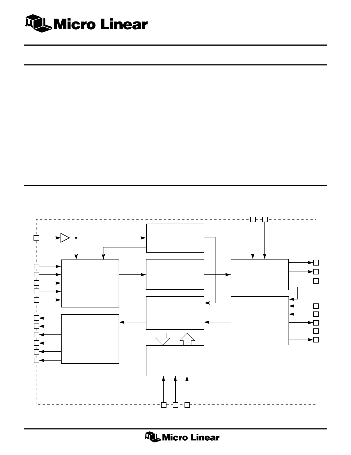
The ML6698 is a high-speed physical layer transceiver
that provides a 5-bit (or symbol) interface to unshielded
twisted pair cable media. The ML6698 is well suited for
adapter card applications using the DEC 21143, the
Macronix MX98713, or equivalent Media Access
Controllers (MACs). The ML6698 may be used in other
100BASE-TX applications requiring the 5-bit interface as
well as FDDI-over-copper applications.
The ML6698 integrates 125MHz clock recovery/
generation, receive adaptive equalization, baseline
wander correction and MLT-3/10BASE-T transmitter.
BLOCK DIAGRAM (PLCC Pin Configuration)
TXC
44
CLOCK SYTHESIZER
FEATURES
■ 5-bit (or symbol) parallel interface
■ Compliant to IEEE 802.3u 100BASE-TX standard
■ Compliant to ANSI X3T12 TP-PMD (FDDI) standard
■ Single-jack 10BASE-T/100BASE-TX solution when used
with external 10Mbps PHY
■ 125MHz receive clock recovery/generation
■ Baseline wander correction
■ Adaptive equalization and MLT-3 encoding/decoding
■ Supports full-duplex operation
*Some Packages Are End Of Life As Of August 1, 2000
41 40
10BTTXINP
10BTTXINN
TSM4
2
TSM3
3
TSM2
4
TSM1
5
TSM0
6
RXC
16
RSM4
8
RSM3
9
RSM2
11
RSM1
13
RSM0
15
SERIALIZER
DESERIALIZER
NRZ TO NRZI
AND
NRZI TO MLT-3
ENCODER
CLOCK AND DATA
RECOVERY
NRZI TO NRZ DECODER
CONTROL LOGIC
PWRDN
LPBK
SEL100/10
74225
100BASE-TX/10BASE-T
TWISTED PAIR DRIVER
EQUALIZER
BLW CORRECTION
MLT-3 DECODER
LOOPBACK MUX
TPOUTP
TPOUTN
CMREF
RGMSET
RTSET
TPINP
TPINN
SDO
34
33
31
38
37
39
30
24
1
Page 2
ML6698
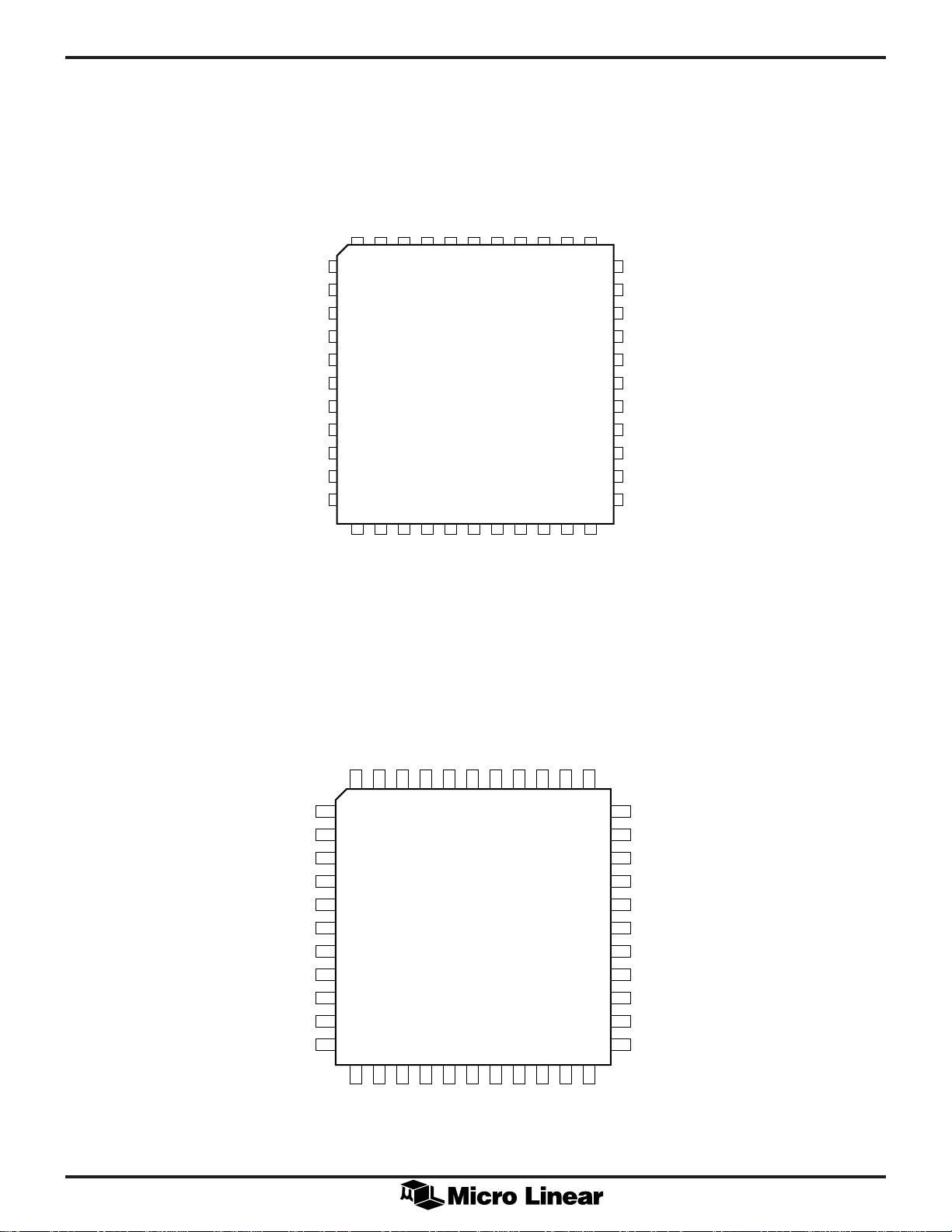
PIN CONFIGURATION
PWRDN
RSM4
RSM3
DGND1
RSM2
DVCC1
RSM1
DGND2
RSM0
RXC
DGND3
44-Pin PLCC (Q44)
TSM0
TSM1
TSM2
TSM3
65432
7
8
9
10
11
12
13
14
15
16
17
18 19 20 21 22
ML6698
TSM4
AGND1
TXC
AVCC1
LPBK
1442543264227412840
23 24
10BTTXINP
10BTTXINN
39
38
37
36
35
34
33
32
31
30
29
CMREF
TPINP
TPINN
AVCC2
AGND2
TPOUTP
TPOUTN
AGND3
RTSET
RGMSET
NC
PWRDN
RSM4
RSM3
DGND1
RSM2
DVCC1
RSM1
DGND2
RSM0
RXC
DGND3
DVCC2
DGND4B
DGND4A
44-Pin TQFP (H44-10)
TSM0
TSM1
TSM2
44 43 42 41 40
1
2
3
4
5
6
7
8
9
10
11
12 13 14 15 16
SDO
DVCC5
DGND5
DGND4C
ML6698
TSM3
TSM4
AGND1
TXC
39 381937203621352234
17 18
SEL100/10
AVCC1
NC
LPBK
NC
AVCC3
10BTTXINP
10BTTXINN
33
32
31
30
29
28
27
26
25
24
23
CMREF
TPINP
TPINN
AVCC2
AGND2
TPOUTP
TPOUTN
AGND3
RTSET
RGMSET
NC
NC
NC
AVCC3
SEL100/10
DVCC2
DGND4A
DGND4B
DGND4C
DVCC5
SDO
DGND5
2
Page 3

ML6698
PIN DESCRIPTION
PIN NAME DESCRIPTION
1 (39) AGND1 Analog ground.
2-6 (40-44) TSM<4:0> Transmit data TTL inputs. TSM<4:0> inputs accept TX data symbols. Data
7 (1) PWRDN Device power down input. A low signal powers down all ciruits of the ML6698, and
8,9, (2, 3, RSM<4:0> Receive data TTL outputs. RSM<4:0> outputs may be sampled synchronously with
11,13, 5, 7, 9) RXC’s rising edge.
15
10 (4) DGND1 Digital ground.
12 (6) DVCC1 Digital +5V power supply.
14 (8) DGND2 Digital ground.
16 (10) RXC Recovered receive symbol clock TTL output. This 25MHz clock is phase-aligned
17 (11) DGND3 Digital ground.
18 (12) DVCC2 Digital +5V power supply.
19 (13) DGND4A Digital ground.
(Pin numbers for TQFP package in parentheses)
appearing at TSM<4:0> are clocked into the ML6698 on the rising edge of TXC.
dissipates less than 20mA.
with the internal 125MHz bit clock recovered from the signal received at TPINP/N
when data is present. Receive data at RSM<4:0> change on the falling edges and
should be sampled on the rising edges of this clock. RXC is phase aligned to TXC
when 100BASE-TX signal is not present at TPINP/N
20 (14) DGND4B Digital ground.
21 (15) DGND4C Digital ground.
22 (16) DVCC5 Digital +5V power supply.
23 (17) DGND5 Digital ground.
24 (18) SD0 Signal detect TTL output. A high output level indicates 100BASE-TX activity at
TPINP/N with an amplitude exceeding the preset threshold. The signal detect
function is always active independent of the configuration of the SEL100/10 pin.
25 (19) SEL100/10 Speed select TTL input. Driving this pin low disables 100BASE-TX transmit and
receive functions, and enables the 10BASE-T transmit path from 10BTTXINP/N to
TPOUTP/N. A high signal on SEL100/10 disables the 10BTTXINP/N inputs and enables
100BASE-TX operation.
28 (22) AVCC3 Analog positive power supply.
30 (24) RGMSET Equalizer bias resistor input. An external 9.53ký, 1% resistor connected between
RGMSET and AGND3 sets internal time constants controlling the receive equalizer
transfer function.
31 (25) RTSET Transmit level bias resistor input. An external 2.49ký, 1% resistor connected
between RTSET and AGND3 sets a precision constant bias current for the twisted
pair transmit level.
32 (26) AGND3 Analog ground.
33,34 (27,28) TPOUTN/P Transmit twisted pair outputs. This differential current output pair drives MLT-3
waveforms into the network coupling transformer in 100BASE-TX mode, and
10BASE-T or FLP waveforms in 10BASE-T mode.
35 (29) AGND2 Analog ground.
36 (30) AVCC2 Analog +5V power supply.
37,38 (31, 32) TPINN/P Receive twisted pair inputs. This differential input pair receives 100BASE-TX signals
from the network.
3
Page 4

ML6698
PIN DESCRIPTION (Continued)
PIN NAME DESCRIPTION
39 (33) CMREF Receiver common-mode reference output. This pin provides a common-mode bias
point for the twisted-pair media line receiver. A typical value for CMREF is
(VCC–1.26)V.
40,41 (34,35) 10BTTXINN/P 10BASE-T transmit waveform inputs. The ML6698 presents a linear copy of the input
at 10BTTXINN/P to the TPOUTN/P outputs when the ML6698 functions in 10BASE-T
mode. Signals presented to these pins must be centered at VCC/2 with a single ended
amplitude of ± 0.25V.
42 (36) LPBK Loopback TTL input pin. Tying this pin to ground places the part in loopback mode;
data at RSM<4:0> are serialized, MLT-3 encoded, equalized then sent to the receive
PLL for clock recovery and sent to the RSM<4:0> outputs. Floating this pin or tying it
to VCC places the part in its normal mode of operation.
43 (37) AVCC1 Analog +5V power supply.
44 (38) TXC Transmit clock TTL input. This 25MHz clock is the frequency reference for the
internal transmit PLL clock multiplier. This pin should be driven by an external
25MHz clock at TTL or CMOS levels.
4
Page 5

ML6698
ABSOLUTE MAXIMUM RATINGS
Junction Temperature ............................................. 150°C
Storage Temperature .............................. ..–65°C to 150°C
Absolute maximum ratings are those values beyond which
Lead Temperature (Soldering, 10 sec) ..................... 260°C
the device could be permanently damaged. Absolute
maximum ratings are stress ratings only and functional
device operation is not implied.
VCC Supply Voltage Range ................... GND –0.3V to 6V
Input Voltage Range
Digital Inputs ....................... GND –0.3V to VCC + 0.3V
TPINP, TPINN, 10BTTXINP,
10BTTXINN ..................... GND –0.3V to VCC + 0.3V
Output Current
TPOUTP, TPOUTN ..............................................60mA
All other outputs ..................................................10mA
OPERATING CONDITIONS
VCC Supply Voltage ............................................ 5V ± 5%
All VCC supply pins
All GND pins
TA, Ambient temperature ................................0°C to 70°C
RGMSET ..................................................... 9.53ký ± 1%
RTSET.......................................................... 2.49ký ± 1%
Receive transformer insertion loss........................ <–0.5dB
must
be within 0.1V of each other.
must
be within 0.1V of each other.
DC ELECTRICAL CHARACTERISTICS
Over full range of operating conditions unless otherwise specified (Note 1)
SYMBOL PARAMETER CONDITIONS MIN TYP MAX UNITS
TTL Inputs (TSM<4:0>, TXC, SEL100/10, PWRDN, LPBK)
V
IL
V
IH
I
IL
I
IH
TTL Outputs (RSM<4:0>, RXC, SDO)
Input Low Voltage I
Input High Voltage I
Input Low Current V
Input High Current V
= –400µA 0.8 V
IL
= 100µA 2.0 V
IH
= 0.4V –200 µA
IN
= 2.7V 100 µA
IN
V
OL
V
OH
Receiver
V
ICM
V
ID
R
IDR
I
ICM
I
RGM
I
RT
Transmitter
I
TD100
I
TD10
I
TOFF
I
TXI
Output Low Voltage I
Output High Voltage I
TPINP/N Input Common-Mode 100ý Termination across TPINP/N VCC – 1.26 V
Voltage
TPINP-TPINN Differential Input –3.0 3.0 V
Voltage Range
TPINP-TPINN Differential 10.0k ý
Input Resistance
TPINP/N Common-Mode Input +10 µA
Current
RGMSET Input Current RGMSET = 9.53ký 130 µA
RTSET Input Current RTSET = 2.49ký 500 µA
TPOUTP/N 100BASE-TX Mode Note 2, 3 ±19 ±21 mA
Differential Output Current
TPOUTP/N 10BASE-T ±55 ±60 ±65 mA
Mode Differential Output Current
TPOUTP/N Off-State Output RL = 200, 1% 0 1.5 mA
TPOUTP/N Differential Output
Current Imbalance RL = 200, 1% 500 µA
= 4mA 0.4 V
OL
= –4mA 2.4 V
OH
5
Page 6

ML6698
DC ELECTRICAL CHARACTERISTICS (Continued)
SYMBOL PARAMETER CONDITIONS MIN TYP MAX UNITS
Transmitter (Continued)
X
ERR
TPOUTP/N Differential Output V
= VCC; Note 3 –5.0 +5.0 %
OUT
Current Error
X
CMP100
V
OCM10
TPOUTP/N 100BASE-X Output V
Current Compliance Error I
TPOUTP/N 10BASE-T Output I
= VCC ± 2.2V; referred to
OUT
at V
OUT
TD10
CC
remains within specified V
–2.0 +2.0 %
– 2.7 V
CC
+ 2.7 V
CC
Voltage Compliance Range values
V
ICM10
10BTTXNN/P Input VCC/2 – 0.3 VCC/2 + 0.3 V
Common-Mode Voltage Range
Power Supply Current
I
CC100
Supply Current, 100BASE-TX Current into all VCC pins, 195 260 mA
Operation, Transmitting VCC = 5.25V (Note 2)
I
CC10
I
CCOFF
Supply Current, 10BASE-T Mode 155 175 mA
Supply Current PWRDN 20 mA
Power Down Mode
AC ELECTRICAL CHARACTERISTICS
Over full range of operating conditions unless otherwise specified
SYMBOL PARAMETER CONDITIONS MIN TYP MAX UNITS
t
TR/F
t
TM
t
TDC
t
TJT
X
OST
t
TXP
t
RXDC
TPOUTP-TPOUTN Differential Notes 5, 6; for any legal 3.0 5.0 ns
Rise/Fall Time code sequence
TPOUTP-TPOUTN Differential Notes 5, 6; for any legal –0.5 0.5 ns
Rise/Fall Time Mismatch code sequence
TPOUTP-TPOUTN Differential Notes 4, 6 –0.5 0.5 ns
Output Duty Cycle Distortion
TPOUTP-TPOUTN Differential Note 6 300 1400 ps
Output Peak-to-Peak Jitter
TPOUTP-TPOUTN Differential Notes 6, 7 5 %
Output Voltage Overshoot
Transmit Bit Delay Note 8 10.5 Bit Times
Receive Bit Delay Note 9 15.5 Bit Times
6
Page 7

ML6698
AC ELECTRICAL CHARACTERISTICS (Continued)
SYMBOL PARAMETER CONDITIONS MIN TYP MAX UNITS
MII (Media-Independent Interface)
X
BTOL
TX Output Clock Frequency 25MHz frequency –100 +100 ppm
Tolerance
t
TPWH
t
TPWL
t
RPWH
t
RPWL
t
TPS
TXC pulse width HIGH 14 ns
TXC pulse width LOW 14 ns
RXC pulse width HIGH 14 ns
RXC pulse width LOW 14 ns
Setup time, TSM<4:0> Data Valid 12 ns
to TXC Rising Edge (1.4V point)
t
TPH
Hold Time, TSM<4:0> Data 3 ns
Valid After TXC Rising Edge
(1.4V point)
t
RCS
Time that RSM<4:0> Data are 10 ns
Valid Before RXC Rising Edge
(1.4V point)
t
RCH
Time that RSM<4:0> Data are 10 ns
Valid After RXC Rising Edge
(1.4V point)
t
RPCR
t
RPCF
Note 1. Limits are guaranteed by 100% testing, sampling, or correlation with worst case test conditions.
Note 2. Measured using the test circuit shown in Fig. 1, under the following conditions:
Note 3. Output current amplitude is I
Note 4. Measured relative to ideal negative and positive signal 50% points, using the four successive MLT-3 transitions for the 01010101 bit sequence.
Note 5. Time difference between 10% and 90% levels of the transition from the baseline voltage (nominally zero) to either the positive or negative peak signal voltage. The
Note 6. Differential test load is shown in fig. 1 (see note 3).
Note 7. Defined as the percentage excursion of the differential signal transition beyond its final adjusted value during the symbol interval following the transition. The
Note 8. Symbol /J/ at TSM <4:0> sampled by TXC to first bit of /J/ at MDI.
Note 9. First bit of /J/ at MDI to first rising edge of RXC after the last part of the /J / appears at RSM <4:0>.
RXC 10% – 90% Rise Time 6ns
RXC 90%-10% Fall Time 6ns
= 200ý, RLS = 49.9ý, R
R
LP
All resistors are 1% tolerance.
times specified here correlate to the transition times defined in the ANSI X3T9.5 TP-PMD Rev 2.0 working draft, section 9.1.6, which include the effects of the
external network coupling transformer and EMI/RFI emissions filter.
adjusted value is obtained by doing a straight line best-fit to an output waveform containing 14 bit-times of no transition preceded by a transition from zero to
either a positive or negative signal peak; the adjusted value is the point at which the straight line fit meets the rising or falling signal edge.
= 2.49ký.
TSET
= 40 3 1.25V/RTSET.
OUT
TPOUTP
TPOUTN
V
CC
R
LP
200Ω
R
LP
200Ω
Figure 1. Test Circuit
2:1
R
49.9Ω
1
2
R
49.9Ω
LS
LS
7
Page 8

ML6698
TXC
TSM<4:0>
RXC
t
TPWH
t
TPWH
t
TPWL
Figure 2.
t
TPWL
t
RPCF
t
TPS
t
TPH
t
RPCR
RSM<4:0>
t
t
RCS
Figure 3.
RCM
8
Page 9

FUNCTIONAL DESCRIPTION
ML6698
TRANSMIT SECTION
100BASE-TX Operation
The transmitter accepts scrambled 5-bit symbols clocked in
at 25MHz and outputs MLT-3 signals onto the twisted-pair
media at 100Mbps. The on-chip transmit PLL converts a
25MHz TTL-level clock at TXC to an internal 125MHz bit
clock. TXC from the ML6698 clocks scrambled transmit
symbols from the MAC into the ML6698's TSM<4:0> input
pins. Symbols from the TSM<4:0> inputs are converted
from parallel to serial form at the 125MHz clock rate. The
serial transmit data is converted to MLT-3 3-level code and
driven differentialy out of the TPOUTP and TPOUTN pins
at nominal ± 2V levels with the proper loads. The
transmitter is designed to drive a center-tapped transformer
with a 2:1 winding ratio, so a differential 400 ohm load is
used on the transformer primary to properly terminate the
100 ohm cable and termination on the secondary. The
transformer’s center tap must be tied to VCC. A 2:1
transformer allows using a ±20mA output current in
100BASE-TX mode. Using a 1:1 transformer would have
required twice the output current and increased the on-chip
power dissipation. An external 2.49kW, 1% resistor at the
RTSET pin creates the correct output levels at TPOUP/N.
10BASE-T
In 10BASE-T mode, the transmitter acts as a linear buffer
with a gain of 10. 10BASE-T inputs (Manchester data and
normal link pulses) at 10BTTXINP/N appear as full-swing
signals at TPOUTP/N in this mode. Inputs to the
10BTTXINP/N pins should have a nominal ±0.25V
differential amplitude and a common-mode voltage of
VCC/2, and should also be waveshaped or filtered to meet
the 10BASE-T harmonic content requirements. The ML6698
does not provide any 10BASE-T transmit filtering.
ML6698 SCHEMATIC
Figure 2 shows a general design where the 5-bit and other
control signals interface to the controller. TXC is
connected to a 25MHz, 100ppm clock oscillator.
Inductors L1 and L2 are for the purpose of improving
return loss.
Capacitor C7 is recommended. It decouples some noise at
the inputs of the ML6698 and improves the Bit Error Rate
(BER) performance of the board.
It is recommended having a 0.1µF capacitor on every V
pin as indicated by C3, 4, 9-12. Also, it is recommended
to split the A
recommended that AGND and DGND planes are large
enough for low inductance. If splitting the two grounds
and keeping the ground planes large enough is not
possible due to board space, you could join them into one
larger ground plane.
DIFFERENCES BETWEEN THE ML6694 AND ML6698
Both parts are pin to pin compatible and perform the same
functions. The only differences are:
1. SDO: The ML6694 has SDO (Signal Detect Output)
active in 100BASE-TX mode only, while the ML6698
has it active in both 10BASE-T and 100BASE-TX
modes.
2. SEL10/100 or SEL100/10: The ML6694 has the
100BASE-TX mode active low and the 10BASE-T
mode active high (SEL10/100). The ML6698 has the
opposite polarity where the 100BASE-TX mode is
active high and the 10BASE-T mode is active low
(SEL100/10).
VCC
and D
, AGND and DGND. It is
VCC
CC
RECEIVE SECTION
The receiver converts 3-level MLT-3 signals from the
twisted-pair media to 5-bit scrambled symbols at
RSM<4:0> with extracted clock at RXC. The adaptive
equalizer compensates for the distortion of up to 140m of
cable and attenuates cable-induced jitter, corrects for DC
baseline wander, and converts the MLT-3 signal to 2-level
NRZ. The receive PLL extracts clock from the equalized
signal, providing additional jitter attenuation, and clocks
the signal through the serial to parallel converter. The
resulting 5-bit symbols appear at RSM<4:0>. The
extracted clock appears at RXC. Resistor RGMSET sets
internal time constants controlling the adaptive equalizer’s
transfer function. RGMSET must be set to 9.53k (1%).
LOOPBACK
Tying LPBK pin low places the part in loopback mode.
Data at TXD<4:0> are serialized, MLT-3 encoded,
equalized, then sent to receive PLL for clock recovery and
sent to the RXD<4:0> outputs.
In this mode, data at TXD<4:0> has to be valid 5-bit
symbol data.
9
Page 10

ML6698
NC
65432
TSM0
7
PWRDN
8
RSM4
9
RSM3
10
DGND1
11
RSM2
12
DVCC1
13
RSM1
14
DGND2
15
CONTROLLER INTERFACE
DVCC
RSM0
16
RXC
17
DGND3
DVCC2
18 19 20 21 22
1
4
U2
23
1442543264227412840
TSM1
TSM2
TSM3
TSM4
ML6698
U1
DGND4A
DGND4B
DGND4C
DVCC5
DGND5
23 24
TXC
AGND1
SDO
INPUT FROM A
INPUT FROM A CONTROLLER,
AVCC1
SEL100/10
10BASE-T PHY
OTHERWISE FLOAT
LPBK
10BTTXINN
10BTTXINP
39
CMREF
38
TPINP
37
TPINN
36
AVCC2
35
AGND2
AGND3
RTSET
NC
AVCC
34
33
32
31
30
29
TPOUTP
TPOUTN
RGMSET
NCNCAVCC3
C1
R2 R1
DVCC
C3 C9 C10 C6
OUTPUTS TO A
10BASE-T PHY
R23
R10
C7
R11
L1
R8
AVCC
R9
L2
C8
1:1
2:1
U5
FB1
FB2
R21
C4 C11 C12
R16 R15
R22
C2
R19
R18
AVCC
++
C5
R17
R20
1
TXTP+
2
TXTP–
3
RXTP+
4
5
6
RXTP–
7
8
RJ45
SHIELD
GROUNDED
R1 2.49kW 1%, 1/8W Surface Mount
R2 9.53kW 1%, 1/8W Surface Mount
R8, R9, 200W 1%, 1/8W Surface Mount
R23
R10, R11 100W 1%, 1/8W Surface Mount
R15-R20 49.9W 5%, 1/8W Surface Mount
R21-R22 75W 5%, 1/8W Surface Mount
C1, C3, 0.1µF Ceramic Chip Cap
C4, C8-C12
C5, C6 10µF Tantalum Cap
Figure 2. ML6698 Typical Applications Circuit
10
C7 10pF Cap
C2 Board Layer Cap (2kV rated)
U1 ML6698 44-PLCC Surface Mount
U2 Clock Oscillator, 25MHz 4-Pin Surface Mount
U5 Bel Transformer Module S558-1287-02,
XFMRS Inc. XF6692TX, or Valor ST6129
(not pin compatible)
FB1, FB2 Fair-Rite SM Bead P/N 2775019447
L1, L2 130nH Inductors rated at 50MHz
Page 11

PHYSICAL DIMENSIONS inches (millimeters)
Package: Q44
0.685 - 0.695
(17.40 - 17.65)
0.650 - 0.656
(16.51 - 16.66)
1
ML6698
44-Pin PLCC
0.042 - 0.056
(1.07 - 1.42)
0.025 - 0.045
(0.63 - 1.14)
(RADIUS)
0.042 - 0.048
(1.07 - 1.22)
12
0.050 BSC
(1.27 BSC)
0.013 - 0.021
(0.33 - 0.53)
1
PIN 1 ID
23
0.026 - 0.032
(0.66 - 0.81)
0.472 BSC
(12.00 BSC)
0.394 BSC
(10.00 BSC)
PIN 1 ID
34
0.165 - 0.180
(4.06 - 4.57)
SEATING PLANE
44-Pin (10 x 10 x 1mm) TQFP
34
0.650 - 0.656
(16.51 - 16.66)
0.148 - 0.156
(3.76 - 3.96)
Package: H44-10
0.685 - 0.695
(17.40 - 17.65)
0.009 - 0.011
(0.23 - 0.28)
0.100 - 0.112
(2.54 - 2.84)
0º - 8º
0.500 BSC
(12.70 BSC)
0.003 - 0.008
(0.09 - 0.20)
0.590 - 0.630
(14.99 - 16.00)
12
0.032 BSC
(0.80 BSC)
0.012 - 0.018
(0.29 - 0.45)
0.394 BSC
(10.00 BSC)
23
0.472 BSC
(12.00 BSC)
0.048 MAX
(1.20 MAX)
0.037 - 0.041
(0.95 - 1.05)
0.018 - 0.030
(0.45 - 0.75)
SEATING PLANE
11
Page 12

ML6698
ORDERING INFORMATION
PART NUMBER TEMPERATURE RANGE PACKAGE
ML6698CQ (End Of Life) 0°C to 70°C 44-PIN PLCC (Q44)
ML6698CH 0°C to 70°C 44-PIN TQFP (H44-10)
© Micro Linear 1997 is a registered trademark of Micro Linear Corporation
Products described in this document may be covered by one or more of the following patents, U.S.: 4,897,611; 4,964,026; 5,027,116; 5,281,862; 5,283,483; 5,418,502; 5,508,570; 5,510,727; 5,523,940;
5,546,017; 5,559,470; 5,565,761; 5,592,128; 5,594,376; Japan: 2598946; 2619299. Other patents are pending.
Micro Linear reserves the right to make changes to any product herein to improve reliability, function or design.
Micro Linear does not assume any liability arising out of the application or use of any product described herein,
neither does it convey any license under its patent right nor the rights of others. The circuits contained in this
data sheet are offered as possible applications only. Micro Linear makes no warranties or representations as to
whether the illustrated circuits infringe any intellectual property rights of others, and will accept no responsibility
or liability for use of any application herein. The customer is urged to consult with appropriate legal counsel
before deciding on a particular application.
12
2092 Concourse Drive
San Jose, CA 95131
Tel: 408/433-5200
Fax: 408/432-0295
Ds6698-01
 Loading...