

Page 1

July 1997
PRELIMINARY
ML6697
100BASE-TX Physical Layer with MII
GENERAL DESCRIPTION
The ML6697 implements the complete physical layer of
the Fast Ethernet 100BASE-TX standard. The ML6697
offers a single-chip per-port solution for MII-based
repeater applications. The ML6697 interfaces to the
controller through the Media Independent Interface (MII).
The ML6697 functionality includes 4B/5B encoding/
decoding, Stream Cipher scrambling/descrambling,
125MHz clock recovery/generation, receive adaptive
equalization, baseline wander correction, and MLT-3
transmitter.
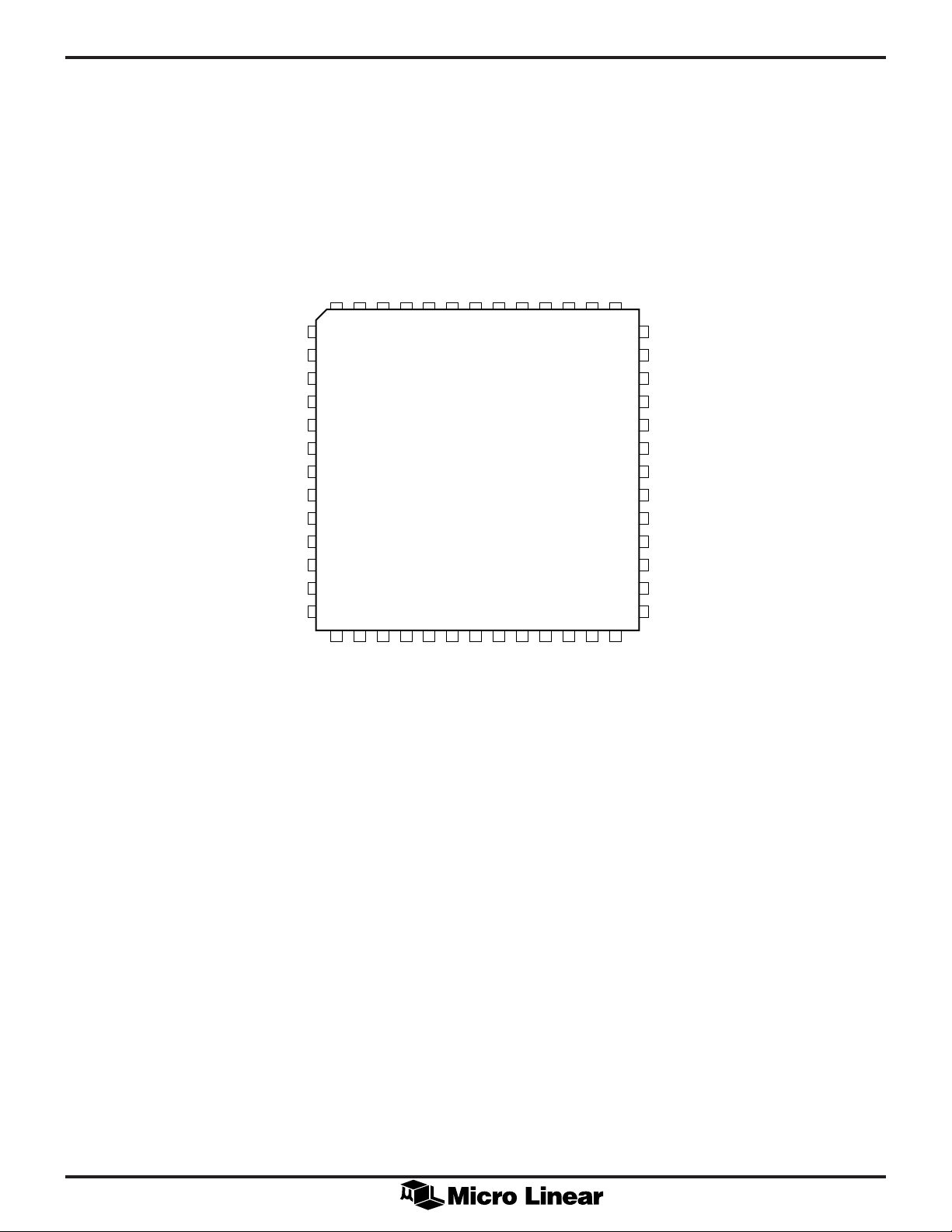
BLOCK DIAGRAM (PLCC Package)
TXCLKIN
1
TXCLK
9
FEATURES
n Single-chip 100BASE-TX physical layer
n Compliant to IEEE 802.3u 100BASE-TX standard
n Supports MII-based repeater applications
n Compliant MII (Media Indendent Interface)
n 4B/5B encoder/decoder
n Stream Cipher scrambler/descrambler
n 125MHz clock recovery/generation
n Baseline wander correction
n Adaptive equalization and MLT-3 encoding/decoding
CLOCK SYNTHESIZER
TXD3
3
TXD2
4
TXD1
5
TXD0
6
TXEN
7
TXER
8
CRS
18
RXEN
19
RXCLK
17
RXD3
10
RXD2
12
RXD1
14
RXD0
16
RXDV
21
RXER
23
PCS TRANSMIT
STATE MACHINE
4B/5B ENCODER
SCRAMBLER
PCS RECEIVE
STATE MACHINE
5B/4B DECODER
DESCRAMBLER
NRZ TO NRZI ENCODER
SERIALIZER
MLT-3 ENCODER
CLOCK AND DATA
RECOVERY
NRZI TO NRZ DECODER
DESERIALIZER
MII MANAGEMENT REGISTERS
AND CONTROL LOGIC
MDIO
MDC
24
25
PHYAD1
PHYAD0
29
PHYAD233PHYAD4
30
31
PHYAD3
32
FLP/100BASE-TX
TWISTED PAIR DRIVER
EQUALIZER
BLW CORRECTION
MLT-3 DECODER
LOOPBACK MUX
TPOUTP
TPOUTN
RTSET
TPINP
TPINN
CMREF
RGMSET
LINK100
40
39
37
45
44
46
36
43
1
Page 2
ML6697
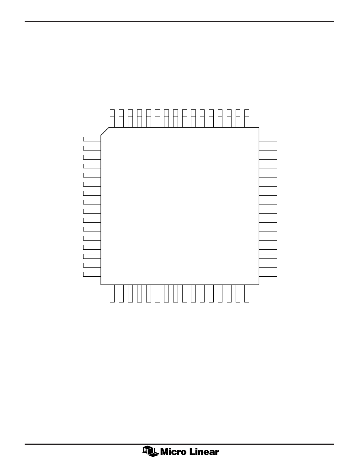
PIN CONFIGURATION
TXCLK
RXD3
DGND1
RXD2
DVCC1
RXD1
DGND2
RXD0
RXCLK
RXEN
DGND3
TXER
CRS
52-Pin PLCC (Q52)
TXEN
TXD0
TXD1
TXD2
76543
8
9
10
11
12
13
14
15
16
17
18
19
20
21 22 23 24 25
ML6697
TXD3
AGND1
TXCLKIN
AVCC1NCNCNCNC
21285229513050314932483347
26 27
NC
46
45
44
43
42
41
40
39
38
37
36
35
34
CMREF
TPINP
TPINN
LINK100
AVCC2
AGND2
TPOUTP
TPOUTN
AGND3
RTSET
RGMSET
AVCC3B
AVCC3A
RXDV
RXER
DVCC2
MDC
MDIO
DVCC5
DGND4
DGND5
PHYAD0
PHYAD1
PHYAD2
PHYAD3
PHYAD4
2
Page 3
PIN CONFIGURATION (Continued)
TXER
TXEN
TXD0
64 63 62 61 60 59 58 57 56 55 54 53 52 51 50 49
TXCLK
RXD3
DGND1A
DGND1B
RXD2
DVCC1A
DVCC1B
RXD1
DGND2A
DGND2B
RXD0
RXCLK
CRS
RXEN
DGND3A
DGND3B
1
2
3
4
5
6
7
8
9
10
11
12
13
14
15
16
17 18 19 20 21 22 23 24 25 26 27 28 29 30 31 32
ML6697
64-Pin TQFP (H64-10)
TXD1
TXD2
TXD3
AGND1A
AGND1B
TXCLKIN
AVCC1NCNC
NC
NC
NC
NC
ML6697
48
47
46
45
44
43
42
41
40
39
38
37
36
35
34
33
NC
CMREF
TPINP
TPINN
LINK100
AVCC2
AGND2A
AGND2B
TPOUTP
TPOUTN
AGND3A
AGND3B
RTSET
RGMSET
AVCC3B
AVCC3A
RXDV
RXER
DVCC2
MDC
MDIO
DGND4B
DGND4A
DVCC5B
DVCC5A
DGND5B
DGND5A
PHYAD0
PHYAD1
PHYAD2
PHYAD3
PHYAD4
3
Page 4

ML6697
PIN DESCRIPTION (Pin numbers for TQFP package in parentheses)
PIN NAME DESCRIPTION
1 (56) TXCLKIN Transmit clock TTL input. This 25MHz clock is the frequency reference for the
internal transmit PLL clock multiplier. This pin should be driven by an external
25MHz clock at TTL or CMOS levels.
2 (58, 57) AGND1 Analog ground.
3, 4 (59,60, TXD<3:0> Transmit data TTL inputs. TXD<3:0> inputs accept TX data from the MII. Data
5, 6 61,62) appearing at TXD<3:0> are clocked into the ML6697 on the rising edge of TXCLK.
7 (63) TXEN Transmit enable TTL input. Driving this input high indicates to the ML6697 that
transmit data are present at TXD<3:0>. TXEN edges should be synchronous with
TXCLK.
8 (64) TXER Transmit error TTL input. Driving this pin high with TXEN also high causes the part
to continuously transmit scrambled H symbols. When TXEN is low, TXER has no
effect.
9 (1) TXCLK Transmit clock TTL output. This 25MHz clock is phase-aligned with the internal
125MHz TX bit clock. Data appearing at TXD<3:0> are clocked into the ML6697 on
the rising edge of this clock.
10, 12, (2, 5, RXD<3:0> Receive data TTL outputs. RXD<3:0> outputs are valid on RXCLK’s rising edge.
14, 16 8, 11)
11 (3, 4) DGND1 Digital ground.
13 (6, 7) DVCC1 Digital +5V power supply.
15 (9, 10) DGND2 Digital ground.
17 (12) RXCLK Recovered receive clock TTL output. This 25MHz clock is phase-aligned with the
internal 125MHz bit clock recovered from the signal received at TPINP/N. Receive
data at RXD<3:0> changes on the falling edges and should be sampled on the rising
edges of this clock. RXCLK is phase aligned to TXCLKIN when the 100BASE-TX
signal is not present at TPINP/N.
18 (13) CRS Carrier Sense TTL output. CRS goes high in the presence of non-idle signals at TPINP/
N. CRS goes low when receive is idle.
19 (14) RXEN Receive enable TTL input. When this input is high, all the MII TTL outputs are
enabled. When this input is low, all the MII TTL outputs are in high impedance
mode. This input does not affect MDIO, TXCLK and CRS.
20 (15, 16) DGND3 Digital ground.
21 (17) RXDV Receive data valid TTL output. This output goes high when the ML6697 is receiving
a data packet. RXDV should be sampled synchronously with RXCLK’s rising edge.
22 (18) DVCC2 Digital +5V power supply.
23 (19) RXER Receive error TTL output. This output goes high to indicate error or invalid symbols
within a packet, or corrupted idle between packets. RXER should be sampled
synchronously with RXCLK’s rising edge.
24 (20) MDC MII Management Interface clock TTL input. A clock at this pin clocks serial data into
or out of the ML6697’s MII management registers through the MDIO pin. The
maximum clock frequency at MDC is 2.5MHz.
4
Page 5

ML6697
PIN DESCRIPTION (Continued)
PIN NAME DESCRIPTION
25 (21) MDIO MII Management Interface data TTL input/output. Serial data are written to and read
from the ML6697’s management registers through this I/O pin. Input data is sampled
on the rising edge of MDC. Data output should be sampled synchronously with
MDC's rising edge.
26 (22, 23) DGND4 Digital ground.
27 (24, 25) DVCC5 Digital +5V power supply.
28 (26, 27) DGND5 Digital ground.
29 (28) PHYAD0 MII Serial Management Interface address bit 0.
30 (29) PHYAD1 MII Serial Management Interface address bit 1.
31 (30) PHYAD2 MII Serial Management Interface address bit 2.
32 (31) PHYAD3 MII Serial Management Interface address bit 3.
33 (32) PHYAD4 MII Serial Management Interface address bit 4.
34 (33) AVCC3A Analog +5V power supply.
35 (34) AVCC3B Analog +5V power supply.
36 (35) RGMSET Equalizer bias resistor input. An external 9.53kW, 1% resistor connected between
RGMSET and AGND3 sets internal time constants controlling the receive equalizer
transfer function.
37 (36) RTSET Transmit level bias resistor input. An external 2.49kW, 1% resistor connected between
RTSET and AGND3 sets a precision constant bias current for the twisted pair transmit
level.
38 (37, 38) AGND3 Analog ground.
39, 40 (39, 40) TPOUTN/P Transmit twisted pair outputs. This differential current output pair drives MLT-3
waveforms into the network coupling transformer.
41 (41, 42) AGND2 Analog ground.
42 (43) AVCC2 Analog +5V power supply.
43 (44) LINK100 100BASE-TX link activity open-drain output. LINK100 pulls low when there is
100BASE-TX activity at TPINP/N in 100BASE-TX or auto-negotiation modes. This
output is capable of driving an LED directly.
44, 45 (45, 46) TPINN/P Receive twisted pair inputs. This differential input pair receives 100BASE-TX signals
from the network.
46 (47) CMREF Receiver common-mode reference output. This pin provides a common-mode bias
point for the twisted-pair media line receiver, typically (VCC – 1.26)V.
52 (55) AVCC1 Analog +5V power supply.
5
Page 6

ML6697
ABSOLUTE MAXIMUM RATINGS
Absolute maximum ratings are those values beyond
which the device could be permanently damaged.
Absolute maximum ratings are stress ratings only and
Thermal Resistance (qJA)
PLCC ............................................................... 40°C/W
TQFP ...............................................................52°C/W
functional device operation is not implied.
VCC Supply Voltage Range .................. GND –0.3V to 6V
Input Voltage Range
OPERATING CONDITIONS
Digital Inputs ...................... GND –0.3V to VCC +0.3V
TPINP, TPINN, .................... GND –0.3V to VCC +0.3V
Output Current
TPOUTP, TPOUTN ............................................. 60mA
All other outputs ................................................. 10mA
Junction Temperature............................................. 150°C
Storage Temperature ..............................–65°C to +150°C
Lead Temperature (Soldering, 10 sec) .................... 260°C
VCC Supply Voltage ........................................... 5V ± 5%
All VCC supply pins
All GND pins
must
be within 0.1V of each other.
must
be within 0.1V of each other.
TA, Ambient temperature.............................. 0°C to 70°C
RGMSET .................................................... 9.53kW ± 1%
RTSET ........................................................ 2.49kW ± 1%
Receive transformer insertion loss ...................... <–0.5dB
DC ELECTRICAL CHARACTERISTICS
Over full range of operating conditions unless otherwise specified (Note 1).
SYMBOL PARAMETER CONDITIONS MIN TYP MAX UNITS
RECEIVER
V
ICM
TPINP/N Input Common-Mode VCC – 1.26 V
Voltage (CMREF)
V
ID
R
IDR
I
ICM
I
RGM
I
RT
LED OUTPUT (LINK100)
I
OLS
I
OHS
TRANSMITTER
I
TD
I
TOFF
I
TXI
X
ERR
TPINP-TPINN Differential Input –3.0 3.0 V
Voltage Range
TPINP-TPINN Differential 10.0k W
Input Resistance
TPINP/N Common-Mode Input +10 µA
Current
RGMSET Input Current RGMSET = 9.53kW 130 µA
RTSET Input Current RTSET = 2.49kW 500 µA
Output Low Current 5mA
Output Off Current 10 µA
TPOUTP/N Note 2, 3 ±19 ±21 mA
Differential Output Current
TPOUTP/N Off-State Output RL = 200, 1% 0 1.5 mA
TPOUTP/N Differential Output
Current Imbalance RL = 200, 1% 500 µA
TPOUTP/N Differential Output V
Current Error
= VCC; Note 3 –5.0 +5.0 %
OUT
X
CMP
TPOUTP/N V
Current Compliance Error I
= VCC ± 2.2V; referred to
OUT
at V
OUT
CC
–2.0 +2.0 %
6
Page 7

ML6697
DC ELECTRICAL CHARACTERISTICS
(Continued)
SYMBOL PARAMETER CONDITIONS MIN TYP MAX UNITS
POWER SUPPLY CURRENT
I
CC
Supply Current, Transmitting Current into all VCC pins 200 300 mA
TTL INPUTS (TXD<3:0>, TXCLKIN, MDC, MDIO, TXEN, TXER, RXEN)
V
IL
V
IH
I
IL
I
IH
Input Low Voltage I
Input High Voltage I
Input Low Current V
Input High Current V
= –400µA 0.8 V
IL
= 100µA 2.0 V
IH
= 0.4V –200 µA
IN
= 2.7V 100 µA
IN
MII TTL OUTPUTS (RXD<3:0>, RXCLK, RXDV, RXER, CRS, MDIO, TXCLK)
V
V
OLT
OHT
Output Low Voltage I
Output High Voltage I
= 4mA 0.4 V
OL
= –4mA 2.4 V
OH
CMOS INPUTS (PHYAD<4:0>)
V
ILC
V
IHC
Note 1. Limits are guaranteed by 100% testing, sampling, or correlation with worst case test conditions.
Input Low Voltage 0.2 x V
Input High Voltage 0.8 x V
CC
CC
V
V
7
Page 8

ML6697
AC ELECTRICAL CHARACTERISTICS
Over full range of operating conditions unless otherwise specified (Note 1).
SYMBOL PARAMETER CONDITIONS MIN TYP MAX UNITS
TRANSMITTER (Note 3)
t
TR/F
TPOUTP-TPOUTN Differential Notes 5, 6; for any legal 3.0 5.0 ns
Rise/Fall Time code sequence
t
TM
TPOUTP-TPOUTN Differential Notes 5, 6; for any legal –0.5 0.5 ns
Rise/Fall Time Mismatch code sequence
t
TDC
TPOUTP-TPOUTN Differential Notes 4, 6 –0.5 0.5 ns
Output Duty Cycle Distortion
t
TJT
TPOUTP-TPOUTN Differential Note 6 300 1400 ps
Output Peak-to-Peak Jitter
X
OST
TPOUTP-TPOUTN Differential Notes 6, 7 5 %
Output Voltage Overshoot
t
t
CLK
TXP
TXCLKIN – TXCLK Delay 6 8 11 ns
Transmit Bit Delay Note 8 10.5 bit times
RECEIVER
t
RXDC
t
RXDR
Receive Bit Delay (CRS) Note 9 15.5 bit times
Receive Bit Delay (RXDV) Note 10 25.5 bit times
MII (Media-Independent Interface)
X
BTOL
TX Output Clock Frequency 25MHz frequency –100 +100 ppm
Tolerance
t
TPWH
t
TPWL
t
RPWH
t
RPWL
t
TPS
TXCLKIN pulse width HIGH 14 ns
TXCLKIN pulse width LOW 14 ns
RXCLK pulse width HIGH 14 18 ns
RXCLK pulse width LOW 14 22 ns
Setup time, TXD<3:0> Data 15 ns
Valid to TXCLK Rising Edge
(1.4V point)
t
TPH
t
RCS
t
RCH
t
RPCR
t
RPCF
t
REND
t
RENZ
8
Hold Time, TXD<3:0> Data 0 ns
Valid After TXCLK Rising Edge
(1.4V point)
Time that RXD<3:0> Data are 10 20 ns
Valid Before RXCLK Rising Edge
(1.4V point)
Time that RXD<3:0> Data are 10 19 ns
Valid After RXCLK Rising Edge
(1.4V point)
RXCLK 10% – 90% Rise Time 6 ns
RXCLK 90%-10% Fall Time 6ns
RXEN high to RXD<3:0>, 2 10 ns
RXDV, RXER, RXCLK Driving
RXEN low to RXD<3:0>, 2 10 ns
RXDV, RXER, RXCLK
High Impedence
Page 9

ML6697
AC ELECTRICAL CHARACTERISTICS (Continued)
SYMBOL PARAMETER CONDITIONS MIN TYP MAX UNITS
MDC-MDIO (MII Management Interface)
t
SPWS
Write Setup Time, MDIO Data 10 ns
Valid to MDC Rising Edge
1.4V Point
t
SPWH
Write Hold Time, MDIO Data 10 ns
Valid After MDC Rising Edge
1.4V Point
t
SPRS
Read Setup Time, MDIO Data 100 ns
Valid to MDC Rising Edge
1.4V Point
t
SPRH
Read Hold Time, MDIO Data 0 ns
Valid After MDC Rising Edge
1.4V Point
t
CPER
t
CPW
Note 1. Limits are guaranteed by 100% testing, sampling, or correlation with worst case test conditions.
Note 2. Measured using the test circuit shown in fig. 1, under the following conditions:
Note 3. Output current amplitude is I
Note 4. Measured relative to ideal negative and positive signal 50% points, using the four successive MLT-3 transitions for the 01010101 bit sequence.
Note 5. Time difference between 10% and 90% levels of the transition from the baseline voltage (nominally zero) to either the positive or negative peak signal voltage. The
Note 6. Differential test load is shown in fig. 1 (see note 2).
Note 7. Defined as the percentage excursion of the differential signal transition beyond its final adjusted value during the symbol interval following the transition. The
Note 8. From first rising edge of TXCLK after TXEN goes high, to first bit of J at the MDI.
Note 9. From first bit of J at the MDI, to CRS.
Note 10. From first bit of J at the MDI, to first rising edge of RXCLK after RXDV goes high.
Period of MDC 400 ns
Pulsewidth of MDC Positive or negative pulses 160 ns
= 200W, RLS = 49.9W, R
R
LP
All resistors are 1% tolerance.
times specified here correlate to the transition times defined in the ANSI X3T9.5 TP-PMD Rev 2.0 working draft, section 9.1.6, which include the effects of the
external network coupling transformer and EMI/RFI emissions filter.
adjusted value is obtained by doing a straight line best-fit to an output waveform containing 14 bit-times of no transition preceded by a transition from zero to
either a positive or negative signal peak; the adjusted value is the point at which the straight line fit meets the rising or falling signal edge.
= 2.49kW.
TSET
= 40 ´ 1.25V/RTSET.
OUT
TPOUTP
TPOUTN
V
CC
R
200Ω
R
200Ω
LP
LP
2:1
R
49.9Ω
1
2
R
LS
LS
49.9Ω
Figure 1.
9
Page 10

ML6697
TXCLKIN
TXCLK
TXD<3:0>
TXER
TXEN
RXCLK
RXD<3:0>
RXER
RXDV
t
TPWH
t
TPS
t
TPH
t
TPWL
Figure 2. MII Transmit Timing
t
RPCR
t
RCS
t
RCH
t
RPCF
MDC
MDIO
MDC
MDIO
Figure 3. MII Receive Timing
t
SPWS
t
SPWH
Figure 4. MII Management Interface Write Timing
t
CPER
t
t
SPRS
SPRH
t
CPW
t
CPW
10
Figure 5. MII Management Interface Read Timing
Page 11

FUNCTIONAL DESCRIPTION
ML6697
TRANSMIT SECTION
The transmitter includes everything necessary to accept
4-bit data nibbles clocked in at 25MHz at the MII and
output scrambled, 5-bit encoded MLT-3 signals into twisted
pair at 100Mbps. The on-chip transmit PLL converts a
25MHz TTL-level clock at TXCLKIN to an internal 125MHz
bit clock. TXCLK from the ML6697 clocks transmit data
from the MAC into the ML6697’s TXD<3:0> input pins
upon assertion of TXEN. Data from the TXD<3:0> inputs are
5-bit encoded, scrambled, and converted from parallel to
serial form at the 125MHz clock rate. The serial transmit
data is converted to MLT-3 3-level code and driven
differentially out of the TPOUTP and TPOUTN pins at
nominal ±2V levels with the proper loads. The transmitter is
designed to drive a center-tapped transformer with a 2:1
winding ratio, so a differential 400W load is used on the
transformer primary to properly terminate the 100W cable
and termination on the secondary. The transformer’s center
tap must be tied to VCC. A 2:1 transformer allows using a
±20mA output current. Using a 1:1 transformer would have
required twice the output current and increased the on-chip
power dissipation. An external 2.49kW, 1% resistor at the
RTSET pin creates the correct output levels at TPOUTP/N.
Driving TXER high when TXEN is high causes the H symbol
(00100) to appear in scrambled MLT-3 form at TPOUTP/N.
The media access controller asserts TXER synchronously
with TXCLK rising edge, and the H symbol appears at least
once in place of a valid symbol in the current packet.
With no data at TXD<3:0> scrambled idle appears at
TPOUTP/N.
RECEIVE SECTION
The receiver includes all necessary functions for
converting 3-level MLT-3 signals from the twisted-pair
media to 4-bit data nibbles at RXD<3:0> with extracted
clock at RXCLK. The adaptive equalizer compensates for
cable distortion and attenuation, corrects for DC baseline
wander, and converts the MLT-3 signal to 2-level NRZ.
The receive PLL extracts clock from the equalized signal,
providing additional jitter attenuation, and clocks the
signal through the serial to parallel converter. The
resulting 5-bit nibbles are descrambled, aligned and
decoded, and appear at RXD<3:0>. The ML6692 asserts
RXDV when it’s ready to present properly decoded
receive data at RXD<3:0>. The extracted clock appears at
RXCLK. Resistor RGMSET sets internal time constants
controlling the adaptive equalizer’s transfer function.
RGMSET must be set to 9.53kW (1%).
The receiver will assert RXER high if it detects code errors
in the receive data packet, or if the idle symbols between
packets are corrupted.
CRS goes high whenever there is non-idle receive activity
in the network.
ML6697 PHY MANAGEMENT FUNCTIONS
The ML6697 has management functions controlled by the
register locations given in Tables 1 and 2. There are two
16-bit MII Management registers, with several unused
locations. Register 0 (Table 1) is the basic control register
(read/write). Register 1 (Table 2) is the basic status register
(read-only). The ML6697 powers on with all management
register bits set to their default values.
See IEEE 802.3u section 22.2.4 for a discussion of MII
management functions and status/control register
definitions.
11
Page 12

ML6697
MII MANAGEMENT INTERFACE REGISTERS
TABLE 1: CONTROL REGISTER
BIT(s) NAME DESCRIPTION R/W DEFAULT
0.15 Reset 1 = reset all register bits to defaults R/W, SC 0
0 = normal operation
0.14 Loopback 1 = PMD loopback mode R/W 0
0 = normal operation
0.13 Manual Speed Select 1 = 100Mb/s RO 1
0 = 10Mb/s
0.11 Power down 1 = power down R/W 0
0 = normal operation
0.12, Not Used RO 0
0.10-0.0
TABLE 2: STATUS REGISTER
BIT(s) NAME DESCRIPTION R/W DEFAULT
1.14 100BASE-TX full duplex 1 = full duplex 100BASE-TX capability RO 0
0 = No full duplex 100BASE-TX capability
1.13 100BASE-TX half duplex 1 = half duplex 100BASE-TX capability RO 1
0 = no half duplex 100BASE-TX capability
1.2 Link status 1 = 100BASE-TX line is up RO/LL latch low after
0 = 100BASE-TX link is down link fail until read
1.0 Extended capability 1 = extended register capabilities RO 0
0 = basic register set only
1.15, Not used RO 0
1.12-1.3,
1.1
NOTE: All unnamed or unused register locations will return a 0 value when accessed.
KEY: LL = latch low until read, R/W = read/write, RO = read only, SC = self-clearing.
12
Page 13

ML6697
AVCC
DVCC
NC
FB1
4
1
U2
C5
++
C4 C11 C12
FB2
C3 C9 C10 C6
23
1234567
D1
NC NC NC NC NC
TXTP+
TXTP–
1:1
R3
NC
NC
NC
49 48 47
NC
50
NC
51
52
21
76543
RXTP+
R10
C1
AVCC1
TXCLKIN
AGND1
TXD3
TXD2
TXD1
TXD0
TXEN
C7
46
CMREF
TXER
8
RXTP–
R11
45
TPINP
TXCLK
9
8
44
TPINN
RXD3
10
RJ45
SHIELD
R16 R15
43
LINK100
DGND1
11
GROUNDED
2:1
L1
R8
42
41
AVCC2
AGND2
RXD2
DVCC1
12
13
R17
R18
R22
40
39
TPOUTP
TPOUTN
U1
ML6697
RXD1
DGND2
14
15
R19
L2
R9
U5
R1
38
AGND3
RXD0
16
R20
37
RXCLK
17
R21
R2
RTSET
18
36
35
RGMSET
CRS
19
C2
C8
34
AVCC3B
AVCC3A
RXEN
DGND3
20
C14
R14
D6
PHYAD4
PHYAD3
PHYAD2
31 32 33
PHYAD1
30
PHYAD0
29
DGND5
28
DVCC5
DGND4
26 27
MDIO
MDC
RXER
DVCC2
RXDV
21 22 23 24 25
D2
D3
R25
R24
C13
R13
D5
8
567
10 9
U6
1234
14 13 12 11
CRS
TXD3
TXD2
Figure 6. Applications Circuit
TXD1
TXD0
TXEN
TXCLK
TXER
RXER
RXCLK
RXDV
RXD0
RXD1
RXD2
RXD3
MII INTERFACE
MDC
MDIO
RXEN
13
Page 14

ML6697
ML6697 SCHEMATIC
Figure 6 shows a general ML6697 design.
The inductors L1 and L2 are for the purpose of improving
return loss. Capacitor C7 is recommended. It decouples
some noise at the inputs of the ML6697, and improves
the Bit Error Rate (BER) performance of the board. We
ML6697 PARTS LIST
COMPONENT DESCRIPTION
U1 ML6697 52-Pin PLCC surface mount
U2 Can Crystal Oscillator, 25MHz 4-pin
surface mount
U5 Transformer Module
U6 HEX Inverter 74HC04
FB1, FB2 Fair-Rite SM Bead P/N 2775019447
L1, L2 130nH inductors rated at 50MHz
recommend having a 0.1µF Cap on every VCC pin as
indicated by C3, 4, 9-12. Also, we recommend splitting
the VCC, AVCC, AGND and DGND. It is recommended
that AGND and DGND planes are large enough for low
inductance. If splitting the two grounds and keeping the
ground planes large enough is not possible due to board
space, you could join them into one larger ground plane.
COMPONENT DESCRIPTION
R10, R11 50W 1% 1/8W surface mount
R13, R14 100kW 10% 1/8W surface mount
R15–R20 49.9W 5% 1/8W surface mount
R21, R22 75W 5% 1/8W surface mount
C1,C3, 0.1µF Ceramic Chip Cap
C4, C8-12
C5, C6 10mF Tantalum Cap.
R1 2.49kW 1% 1/8W surface mount
R2 9.53kW 1% 1/8W surface mount
R3, R24, R25 750W 5% 1/8W surface mount
R8, R9 200W 1% 1/8W surface mount
C7 10pF Cap
C2 Board layer Cap (2V rated)
C13, C14 22nF Cap
D1-D3 LED Diodes
D5-D6 Diodes Phillips PMLL 4148
14
Page 15

PHYSICAL DIMENSIONS inches (millimeters)
0.785 - 0.795
(19.94 - 20.19)
0.750 - 0.754
(19.05 - 19.15)
1
ML6697
Package: Q52
52-Pin PLCC
0.042 - 0.056
(1.07 - 1.42)
0.025 - 0.045
(0.63 - 1.14)
(RADIUS)
0.042 - 0.048
(1.07 - 1.22)
14
0.050 BSC
(1.27 BSC)
0.013 - 0.021
(0.33 - 0.53)
PIN 1 ID
27
0.026 - 0.032
(0.66 - 0.81)
40
0.165 - 0.180
(4.06 - 4.57)
SEATING PLANE
0.750 - 0.754
(19.05 - 19.15)
0.148 - 0.156
0.785 - 0.795
(19.94 - 20.19)
(3.76 - 3.96)
0.009 - 0.011
(0.23 - 0.28)
0.100 - 0.110
(2.54 - 2.79)
0.600 BSC
(15.24 BSC)
0.690 - 0.730
(17.53 - 18.54)
15
Page 16

ML6697
PHYSICAL DIMENSIONS inches (millimeters)
Package: H64-10
64-Pin (10 x 10 x 1mm) TQFP
0.472 BSC
(12.00 BSC)
0.394 BSC
(10.00 BSC)
49
0º - 8º
0.003 - 0.008
(0.09 - 0.20)
1
17
0.020 BSC
(0.50 BSC)
PIN 1 ID
0.007 - 0.011
(0.17 - 0.27)
0.394 BSC
(10.00 BSC)
33
0.472 BSC
(12.00 BSC)
0.048 MAX
(1.20 MAX)
0.037 - 0.041
(0.95 - 1.05)
0.018 - 0.030
(0.45 - 0.75)
SEATING PLANE
ORDERING INFORMATION
PART NUMBER TEMPERATURE RANGE PACKAGE
ML6697CQ 0°C to 70°C 52-Pin PLCC (Q52)
ML6697CH 0°C to 70°C 64-Pin TQFP (H64-10)
Micro Linear makes no representations or warranties with respect to the accuracy, utility, or completeness of the contents
of this publication and reserves the right to make changes to specifications and product descriptions at any time without
notice. No license, express or implied, by estoppel or otherwise, to any patents or other intellectual property rights is granted
by this document. The circuits contained in this document are offered as possible applications only. Particular uses or
applications may invalidate some of the specifications and/or product descriptions contained herein. The customer is urged
to perform its own engineering review before deciding on a particular application. Micro Linear assumes no liability
whatsoever, and disclaims any express or implied warranty, relating to sale and/or use of Micro Linear products including
liability or warranties relating to merchantability, fitness for a particular purpose, or infringement of any intellectual property
right. Micro Linear products are not designed for use in medical, life saving, or life sustaining applications.
© Micro Linear 2000. is a registered trademark of Micro Linear Corporation. All other trademarks are the
property of their respective owners.
Products described herein may be covered by one or more of the following U.S. patents: 4,897,611; 4,964,026; 5,027,116;
5,281,862; 5,283,483; 5,418,502; 5,508,570; 5,510,727; 5,523,940; 5,546,017; 5,559,470; 5,565,761; 5,592,128; 5,594,376;
5,652,479; 5,661,427; 5,663,874; 5,672,959; 5,689,167; 5,714,897; 5,717,798; 5,742,151; 5,747,977; 5,754,012; 5,757,174;
5,767,653; 5,777,514; 5,793,168; 5,798,635; 5,804,950; 5,808,455; 5,811,999; 5,818,207; 5,818,669; 5,825,165; 5,825,223;
5,838,723; 5.844,378; 5,844,941. Japan: 2,598,946; 2,619,299; 2,704,176; 2,821,714. Other patents are pending.
2092 Concourse Drive
San Jose, CA 95131
Tel: 408/433-5200
Fax: 408/432-0295
16
DS6697-01
 Loading...