

Page 1
December 1998
ML6696*
100BASE-X Fiber Physical Layer
GENERAL DESCRIPTION
The ML6696 implements the complete physical layer of
the Fast Ethernet 100BASE-X standard for fiber media. The
device provides the MII (Media Independent Interface) for
interface to upper-layer silicon. The ML6696 integrates the
data quantizer and the LED driver, allowing the use of
low cost optical PMD components.
The ML6696 includes 4B/5B encoder/decoder, 125MHz
clock recovery/clock generation, LED driver, and a data
quantizer. The device also offers a power down mode
which results in total power consumption of less than 20mA.
The ML6696 is suitable for the current 100BASE-FX IEEE
803.2u standard defined using 1300nm optics, as well as
for the
proposed
100BASE-SX standard defined using lower
cost 820nm optics
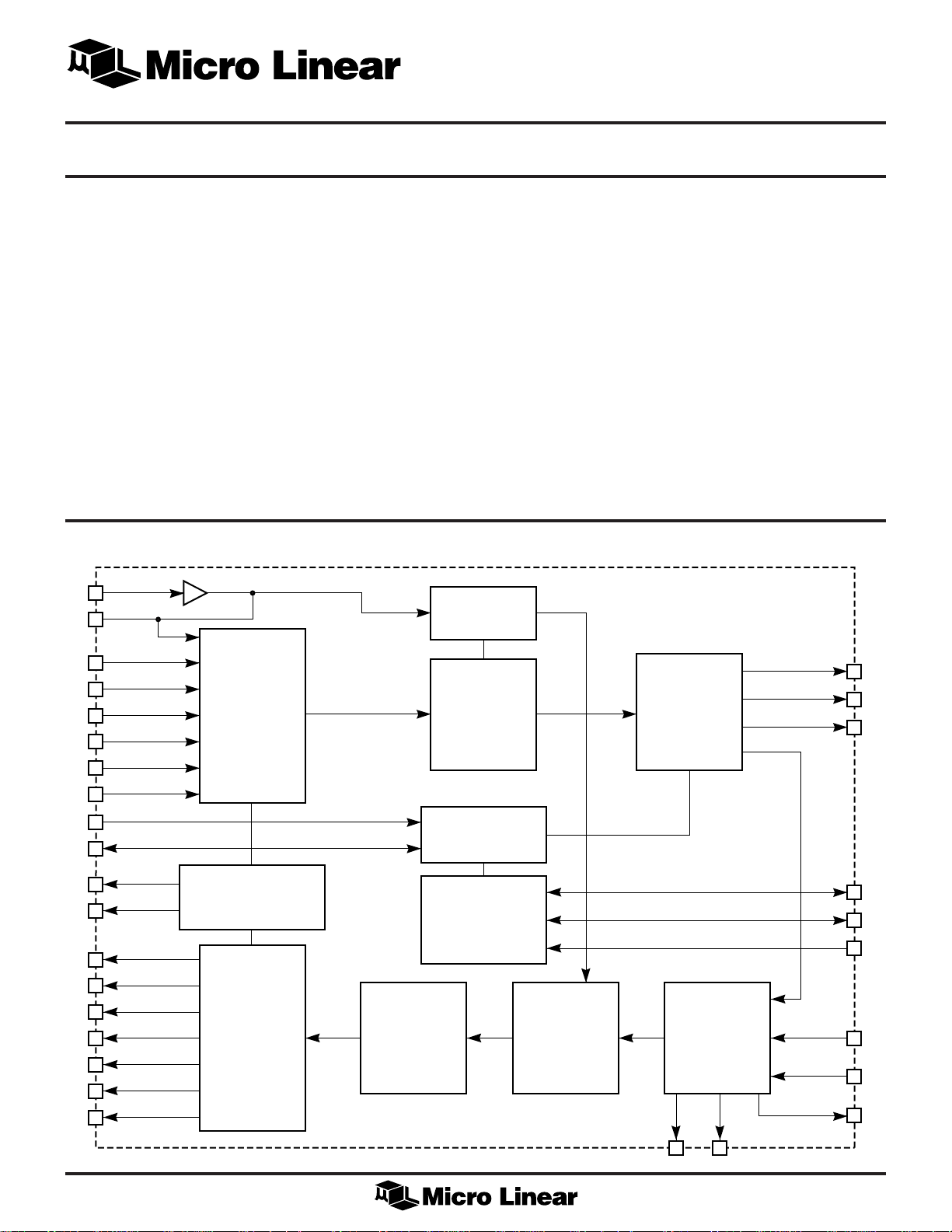
BLOCK DIAGRAM
CLKREF
TXCLK
TXER
TXEN
TXD3
TXD2
TXD1
TXD0
PCS
TRANSMIT
STATE
MACHINE
AND
4B/5B ENCODER
FEATURES
■ 100BASE-FX physical layer with MII
■ Optimal 100BASE-SX solution (draft standard)
■ Integrated data quantizer (post-amplifier)
■ Integrated LED driver
■ 125MHz clock generation and recovery
■ 4B/5B encoding/decoding
■ Power-down mode
* Some Packages Are Obsolete
CLOCK
SYNTHESIZER
SERIALIZER
NRZ TO NRZI
ENCODER
LED
DRIVER
IOUT
IOUT
RTSET
MDC
MDIO
COL
CRS
RXCLK
RXER
RXDV
RXD3
RXD2
RXD1
RXD0
CARRIER & COLLISION
LOGIC
PCS
RECEIVE
STATE
MACHINE
AND
4B/5B DECODER
DESERIALIZER
MII SERIAL
MANAGEMENT
INTERFACE
INITIALIZATION
INTERFACE
CLOCK & DATA
RECOVERY
NRZI TO NRZ
ENCODER
DATA QUANTIZER
(POST AMPLIFIER)
CAPDCCAPB
ECLK
EDIN
EDOUT
V
IN+
V
IN–
LINK100
1
Page 2
ML6696
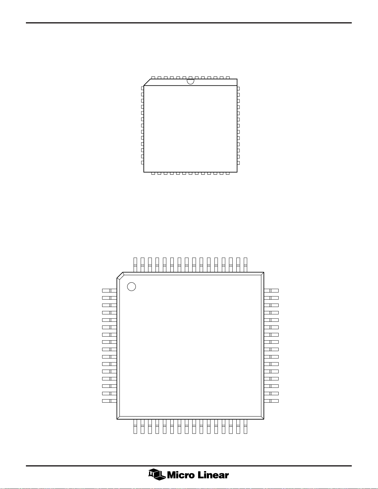
PIN CONFIGURATION
TXER
TXCLK
RXD3
DGND1
RXD2
DVCC1
RXD1
DGND2
RXD0
RXCLK
CRS
COL
DGND3
ML6696
52-Pin PLCC (Q52)
1
CC
EDIN
TXEN
TXD0
TXD1
TXD2
TXD3
AGND1
CLKREF
7654321525150494847
8
9
10
11
12
13
14
15
16
17
18
19
20
21 22 23 24 25 26 27 28 29 30 31 32 33
MDIO
DGND4
5
DV
2
RXDV
DV
CC
RXER
MDC
TOP VIEW
AV
CC
DGND5
NC
ECLK
NC
2
CC
EDOUT
AV
CAPB
CAPDC
AGND2
IOUT
46
45
IOUT
44
AGND3
43
RTSET
42
AVCC3A
41
AVCC3B
40
AVCC4A
39
AGND4A
38
LINK100
37
AVCC4B
36
AVCC4B
35
V
34
V
AGND4B
IN+
IN–
TXCLK
RXD3
DGND1
DGND1
DGND1
RXD2
DVCC1
RXD1
DGND2
DGND2
DGND2
RXD0
RXCLK
CRS
COL
DGND3
ML6696
64-Pin TQFP (H64-10)
1
TXER
TXEN
TXD0
TXD1
TXD2
TXD3
64 63 62 61 60 595857 56 55 54 535251 50 49
1
2
3
4
5
6
7
8
9
10
11
12
13
14
15
16
17 18
19 20 21 222324 25 26 27 282930 31 32
AGND1
CLKREF
AV
CC
EDIN
ECLK
EDOUT
AVCC2
AGND2
AGND2
AGND2
48
47
46
45
44
43
42
41
40
39
38
37
36
35
34
33
IOUT
IOUT
IOUT
IOUT
AGND3
AGND3
RTSET
AVCC3A
AVCC3B
AVCC4A
AGND4A
LINK100
AVCC4B
AVCC4B
V
IN+
V
IN–
RXDV
DGND3
2
CC
DV
RXER
MDC
MDIO
DGND4
5
CC
DV
DGND5
DGND5
NC
NC
CAPB
CAPDC
AGND4B
AGND4B
TOP VIEW
2
Page 3

PIN DESCRIPTION (Pin Number in Parentheses is for PLCC Version)
ML6696
PIN NAME FUNCTION
1 (9) TXCLK Transmit clock TTL output. This
25MHz clock is phase-aligned
with the internal 125MHz TX bit
clock. Data appearing at
TXD<3:0> are clocked into the
ML6696 on the rising edge of this
clock.
2 (10) RXD3 Receive data TTL output. Output
is valid on RXCLK’s rising edge.
3, 4,
5, (11) DGND1 Digital ground
6 (12) RXD2 Receive data TTL output. Output
is valid on RXCLK’s rising edge.
7 (13) DVCC1 Digital positive power supply
8 (14) RXD1 Receive data TTL output. Output
is valid on RXCLK’s rising edge.
9, 10,
11 (15) DGND2 Digital ground
12 (16) RXD0 Receive data TTL output. Output
is valid on RXCLK’s rising edge.
13 (17) RXCLK Recovered receive clock TTL
output. This 25MHz clock is
phase-aligned with the internal
125MHz bit clock recovered from
the signal received at VIN+/-.
Receive data are clocked out at
RXD<3:0> on the falling edges of
this clock, and should be sampled
on rising edges. RXCLK is phasealigned to CLKREF in the absence
of a 100BASE-FX signal at V
14 (18) CRS Carrier Sense TTL output. CRS
goes high in the presence of nonidle signals at VIN+/-, or when the
ML6696 is transmitting. CRS goes
low when there is no transmit
activity and receive is idle. In
repeater or full-duplex mode, CRS
goes high in the presence of nonidle signals at V
15 (19) COL Collision Detected TTL output.
COL goes high upon detection of
a collision on the network, and
remains high as long as the
collision condition persists. COL is
low when the ML6696 operates in
full-duplex, repeater, or loopback
modes.
IN+/–
only.
IN+/–
PIN NAME FUNCTION
16, 17
(20) DGND3 Digital ground
18 (21) RXDV Receive data valid TTL output.
This output is high when the
ML6696 is receiving a data
packet. RXDV is valid on RXCLK’s
rising edge.
19 (22) DVCC2 Digital positive power supply
20 (23) RXER Receive error TTL output. This
output goes high to indicate error
or invalid symbols within a
packet, or corrupted idle between
packets. RXER is valid on RXCLK’s
rising edge.
21 (24) MDC MII Serial Management Interface
clock TTL input. A clock at this
pin clocks serial data into or out
of the ML6696’s MII management
registers through the MDIO pin.
The maximum clock frequency at
MDC is 2.5MHz.
22 (25) MDIO MII Serial Management Interface
data TTL input/output. Serial data
are written to and read from the
management registers through this
I/O pin. Input data is sampled on
the rising edge of MDC. Output
data is valid on MDC's rising edge
23 (26) DGND4 Digital ground
24 (27) DVCC5 Digital positive power supply
.
25, 26
(28) DGND5 Digital ground
27, 28
(29, 30) NC No connect
29 (31) CAPDC Data quantizer offset-correction
loop, offset-storage capacitor input
pin. The capacitor tied between
this pin and AVCC stores the
amplified data quantizer offset
voltage and also sets the dominant
pole in the offset-correction loop.
A 0.1µF surface mount is
recommended.
3
Page 4

ML6696
PIN DESCRIPTION (Pin Number in Parentheses is for PLCC Version) (Continued)
PIN NAME FUNCTION
30 (32) CAPB Data quantizer input bias bypass
capacitor input. The capacitor tied
between this pin and AVCC filters
the quantizer’s internal input bias
reference. A 0.1µF surface-mount
capacitor is recommended.
31, 32
(33) AGND4B Analog ground
33 (34) V
34 (35) V
35, 36
(36, 37) AVCC4B Analog positive power supply
37 (38) LINK100 100BASE-FX link activity open-
38 (39) AGND4A Analog ground
39 (40) AVCC4A Analog positive power supply
40 (41) AVCC3B Analog positive power supply
41 (42) AVCC3A Analog positive power supply
42 (43) RTSET Transmit level bias resistor. For
43, 44
(44) AGND3 Analog ground
IN–
IN+
Receive quantizer negative input.
This input should be tied to
AVCCQ through an AC coupling
capacitor. (0.01µF recommended)
Receive quantizer positive input.
This input receives 100BASE-FX
signals from the network optical
receiver through an AC coupling
capacitor. (0.01µF recommended).
drain output. LINK100 pulls low
when there is 100BASE-FX activity
at VIN+/–. This output is capable
of sinking sufficient current to
directly drive a status LED in
series with a current limiting
resistor.
100BASE-FX, an external 2.32kW,
1% resistor connected between
RTSET and AGND3 sets a
precision constant bias current
that gives a nominal output "on"
current of 75mA at I
OUT
.
PIN NAME FUNCTION
47, 48
(46) IOUT Transmit LED output. This open-
collector current output drives
NRZI waveforms into a network
LED.
49, 50,
51 (47) AGND2 Analog ground
52 (48) AVCC2 Analog positive power supply
53 (49) EDOUT Initialization Interface data out
CMOS input. With EDIN low at
power up, EDOUT has no
function. With EDIN floating at
power up, EDOUT is the serial
data input for configuration data
from an EEPROM. With EDIN high
at power up, EDOUT is the input
for configuration data from an
external microcontroller. (Table 1)
54 (50) ECLK Initialization Interface clock
CMOS input/output. With EDIN
low at power up, ECLK is inactive.
With EDIN floating at power up,
ECLK is the ML6696’s clock
output for timing the configuration
data from an external EEPROM.
With EDIN high at power up,
ECLK is the clock input for timing
configuration data from an
external microcontroller. (Table 1)
55 (51) EDIN Initialization Interface mode
select and EEPROM interface data
in CMOS input/output. EDIN
selects one of three possible
interface modes at power up. See
the Initialization Interface section
for more information. (Table 1)
56 (52) AVCC1 Analog positive power supply
57 (1) CLKREF Transmit clock TTL input. This
25MHz clock is the frequency
reference for the internal TX PLL
clock synthesizer and logic. This
pin should be driven by an
external 25MHz clock at TTL
levels.
45, 46
(45) IOUT Transmit LED output. This pin
connects through an external 15W
resistor to AVCC when the part is
used to drive a network LED.
4
58 (2) AGND1 Analog ground
59 (3) TXD3 Transmit data TTL input. TXD<3:0>
inputs accept TX data symbols from
the MII. Data appearing at TXD<3:0>
are clocked into the ML6696 on the
rising edge of TXCLK.
Page 5

PIN DESCRIPTION (Pin Number in Parentheses is for PLCC Version) (Continued)
ML6696
PIN NAME FUNCTION
60 (4) TXD2 Transmit data TTL input. TXD<3:0>
inputs accept TX data symbols
from the MII. Data appearing at
TXD<3:0> are clocked into the
ML6696 on the rising edge of
TXCLK.
61 (5) TXD1 Transmit data TTL input. TXD<3:0>
inputs accept TX data symbols
from the MII. Data appearing at
TXD<3:0> are clocked into the
ML6696 on the rising edge of
TXCLK.
62 (6) TXD0 Transmit data TTL input. TXD<3:0>
inputs accept TX data symbols
from the MII. Data appearing at
TXD<3:0> are clocked into the
ML6696 on the rising edge of
TXCLK.
PIN NAME FUNCTION
63 (7) TXEN Transmit enable TTL input. Driving
this input high indicates to the
ML6696 that transmit data are
present at TXD<3:0>. TXEN edges
should be synchronous with
TXCLK.
64 (8) TXER Transmit error TTL input. Driving
this pin high with TXEN also high
causes the part to continuously
transmit an H symbol (00100).
When TXEN is low, TXER has no
effect.
5
Page 6

ML6696
ABSOLUTE MAXIMUM RATINGS
Absolute maximum ratings are those values beyond which
the device could be permanently damaged. Absolute
maximum ratings are stress ratings only and functional
device operation is not implied.
Storage Temperature................................. –65ºC to 150ºC
Lead Temperature (Soldering, 10 sec) ..................... 260ºC
Thermal Resistance (qJA)
TQFP ............................................................... 52°C/W
PLCC ............................................................... 40°C/W
VCC Supply Voltage Range ............................–0.3V to 6V
Input Voltage Range
Digital Inputs ........................................... –0.3V to V
VIN+, VIN-, CLKREF, CAPB, CAPDC ........ –0.3V to V
CC
CC
Output Current
IOUT, IOUT ........................................................ 90mA
All Other Outputs ............................................... 10mA
Junction Temperature ....................................0ºC to 125ºC
OPERATING CONDITIONS
Temperature Range ....................................... 0ºC to 70ºC
RTSET ..........................................................2.32kW ±1%
VCC Supply Voltage ......................................... 5V ±5%
All VCC supply pins
All GND pins
must
be within 0.1V of each other.
must
be within 0.1V of each other.
DC ELECTRICAL CHARACTERISTICS
Unless otherwise specified, VCC = 5V ±5%, TA = Operating Temperature Range (Note 1)
SYMBOL PARAMETER CONDITIONS MIN TYP MAX UNITS
TTL INPUTS (TXD<3:0>, CLKREF, MDC, MDIO, TXEN, TXER)
V
V
I
I
TTL OUTPUTS (RXD<3:0>, RXCLK, RXDV, RXER, CRS, COL, MDIO, TXCLK)
Input Low Voltage I
IL
Input High Voltage I
IH
Input Low Current V
IL
Input High Current V
IH
= –400µA -0.3 0.8 V
IL
= 100µA 2.0 VCC+0.3 V
IH
= 0.4V -200 µA
IN
= 2.4V 100 µA
IN
V
V
CMOS INPUTS (EDIN, EDOUT, ECLK)
V
V
IHC
CMOS OUTPUTS (ECLK)
V
OLC
V
OHC
RECEIVER (V
V
ICM
V
R
IDR
V
SDA
A
HYST
OL
OH
ILC
ID
Output Low Voltage I
Output High Voltage I
Input Low Voltage 0.2 ´ V
Input High Voltage 0.8 ´ V
Output Low Voltage IOL = 2mA 0.1 ´ V
Output High Voltage IOL = –2mA 0.9 ´ V
, V
IN–
)
IN+
Input Common-Mode Voltage VCC = 5V 2.5 V
Differential Input Voltage Range 3.5 1600 mV
Differential Input Resistance 500 1000 W
Signal Detect Assertion Threshold Peak-to-Peak Non-idle Signal 8 12 mV
Input Hysteresis 1.5 2 dB
= 4mA 0.4 V
OL
= –4mA 2.4 V
OH
CC
CC V
Level at V
IN+/-
CC
CC
V
V
V
P-P
P-P
6
Page 7

ML6696
DC ELECTRICAL CHARACTERISTICS (Continued)
SYMBOL PARAMETER CONDITIONS MIN TYP MAX UNITS
TRANSMITTER (IOUT, IOUT)
I
LEDH
I
LEDL
I
RT
IOUT High Output Current RTSET = 2.32kW ±1% 67.5 75 82.5 mA
Low Output Current RTSET = 2.32kW ±1% 0.1 mA
RTSET Input Current RTSET = 2.32kW ±1% 486 540 594 µA
POWER SUPPLY CURRENT
I
CC
I
CCPD
Supply Current, 100BASE-FX, Transmitting Current into All VCC Pins 200 295 mA
Supply Current, Power-Down Mode Current into All VCC Pins 20 mA
AC ELECTRICAL CHARACTERISTICS
Unless otherwise specified, VCC = 5V ±5%, TA = Operating Temperature Range (Note 1)
SYMBOL PARAMETER CONDITIONS MIN TYP MAX UNITS
TRANSMITTER
t
CLK
t
TXP
t
TR/F
t
TDCIOUT
RECEIVER
CLKREF – TXCLK Delay 5 11 ns
Transmit Bit Delay Note 2 10.5 bit times
I
Rise /Fall Time Note 3 2 ns
OUT
Output Duty Cycle Disotrtion Note 3 –0.5 0.5 ns
t
RXDC
t
RXDR
Receive Bit Delay (CRS) Note 3 15.5 bit times
Receive Bit Delay (RXDV) Note 4 25.5 bit times
MII INTERFACE
X
NTOL
t
TPWH
t
TPWL
t
RPWH
t
RPWL
t
TPS
CLKREF Input Clock Frequency Tolerance 25MHz Frequency –50 50 ppm
TXCLK Pulse Width High 14 ns
TXCLK Pulse Width Low 14 ns
RXCLK Pulse Width High 14 ns
RXCLK Pulse Width Low 14 ns
Setup Time, TXD<3:0> Data Valid to Note 5 5 ns
TXCLK Rising Edge
t
TPH
Hold time, TXD<3:0> Data Valid Note 5 0 ns
After TXCLK Rising Edge
t
RCS
Time That RXD<3:0> Data are Valid Note 6, 7 10 ns
Before RXCLK Rising Edge
t
RCH
Time That RXD<3:0> Data are Valid Note 6, 7 10 ns
After RXCLK Rising Edge
t
RPCR
t
RPCF
RXCLK 10%-90% Rise Time 6ns
RXCLK 90%-10% Fall Time 6ns
7
Page 8

ML6696
AC ELECTRICAL CHARACTERISTICS (Continued)
SYMBOL PARAMETER CONDITIONS MIN TYP MAX UNITS
MII MANAGEMENT INTERFACE (MDC, MDIO)
t
SPWS
Write Setup Time, MDIO Data Valid 10 ns
to MDC Rising Edge (1.4V Point)
t
SPWH
Write Hold Time, MDIO Data Valid 10 ns
After MDC Rising Edge (1.4V Point)
t
SPRS
Read Setup Time, MDIO Data Valid 100 ns
to MDC Rising Edge (1.4V Point)
t
SPRH
Read Hold Time, MDIO Data Valid 0 ns
After MDC Rising Edge (1.4V Point)
t
CPER
t
CPW
Period of MDC 400 ns
Pulsewidth of MDC Positive or Negative Pulses 160 ns
EEPROM INTERFACE (ECLK, EDIN, EDOUT)
t
PW1
t
PW2
t
PER1
t
DV1
ECLK Positive Pulsewidth EDIN Floating (EEPROM Mode) 900 ns
ECLK Negative Pulsewidth EDIN Floating (EEPROM Mode) 900 ns
ECLK Period EDIN Floating (EEPROM Mode) 1800 ns
EDOUT Data Valid Time EDIN Floating (EEPROM Mode) 900 ns
After ECLK Rising Edge
t
PER2
t
PW3
t
PW4
t
t
H1
Note 1: Limits are guaranteed by 100% testing, sampling, or correlation with worst case test conditions.
Note 2: From first rising edge of TXCLK after TXEN goes high, to first bit of J at the MDI.
Note 3: From first bit of J at the MDI, to CRS.
Note 4: From first bit of J at the MDI, to first rising edge of RXCLK after RXDV goes high.
Note 5: Measured between the time that TXD0-3 transition above or below the region 0.8V–2.0V, and the time that TXCLK rises above 0.8V.
Note 6: Measured between the time that RXD0-3 transition above or below the region 0.8V–2.0V, and the time that RXCLK rises above 0.8V.
Note 7: Measured using a 15pF load to ground.
ECLK Period EDIN High (Microcontroller Mode) 5000 ns
ECLK Positive Pulsewidth EDIN High (Microcontroller Mode) 2000 ns
ECLK Negative Pulsewidth EDIN High (Microcontroller Mode) 2000 ns
ECLK Data Setup Time EDIN High (Microcontroller Mode) 10 ns
S1
ECLK Data Hold Time EDIN High (Microcontroller Mode) 10 ns
8
Page 9

TXCLKIN
ML6696
TXCLK
TXD<3:0>
TXER
TXEN
RXCLK
t
TPWH
t
TPS
t
TPH
t
TPWL
Figure 1. MII Transmit Timing
t
RPCR
t
RPCF
RXD<3:0>
RXER
RXDV
MDC
MDIO
t
RCS
t
RCH
Figure 2. MII Receive Timing
t
SPWS
t
SPWH
Figure 3. MII Management Interface Write Timing
9
Page 10

ML6696
MDC
MDIO
t
CPER
t
t
SPRS
SPRH
t
CPW
t
CPW
Figure 4. MII Management Interface Read Timing
(DRIVEN BY ML6696)
ECLK
EDIN
(DRIVEN BY ML6696)
EDOUT
(DRIVEN BY EEPROM)
t
PW1
01
02 03 04 05 06 07 08 09 10 11
SB1OP11OP00A50A40A30A20A10A0
t
PW2
Figure 5. EEPROM Interface Timing
t
PW3
(INPUT TO ML6696)
ECLK
EDOUT
(INPUT TO ML6696)
01 02 16
t
S1
t
PER1
12 13 26
0
D0 D1 D2 D3 D14 D15
t
DV1
16 BITS DATA ADDRESS
t
PER2
t
PW4
10
H
Figure 6. MII Management Interface Read Timing
Page 11

FUNCTIONAL DESCRIPTION
ML6696
FIBER OPTIC TRANSMITTER
The on-chip transmit PLL converts a 25MHz TTL-level
clock at CLKREF to an internal 125MHz bit clock. TXCLK
from the ML6696 clocks transmit data from the MAC into
the ML6696’s TXD<3:0> input pins upon assertion of
TXEN. Data from the TXD<3:0> inputs are 5-bit encoded
and converted from parallel to serial form at the 125MHz
clock rate. The ML6696 drives corresponding NRZI data
out from its LED driver. The LED driver at IOUT is a
current mode switch which develops the output light by
sinking current through the network LED into IOUT.
RTSET’s value determines the output current:
V
125
.
RTSET
where IOUT is the desired output current.
Driving TXEN low will cause the ML6696’s transmitter to
enter the idle state and output 62.5MHz idle signal.
Driving TXER high when TXEN is high causes the H
symbol (00100) to appear in the transmitted data stream.
The media access controller asserts TXER synchronously
with TXCLK’s rising edge, and the H symbol appears in
place of valid symbols in the current frame.
FIBER OPTIC RECEIVER
=
IOUT
´
140
W
(1)
ML6696 PHY MANAGEMENT FUNCTIONS
The ML6696 has management functions controlled by the
register locations given in Table 3 (page 12). There are
two 16-bit management registers, with several unused
locations. Register 0 is the basic control register (read/
write). Register 1 is the basic status register (read-only).
The ML6696 powers on with all management register bits
set to their default values.
The ML6696’s status and control register addresses and
functions match those described for the MII in IEEE
802.3u section 22. IEEE 802.3u specifies the management
data frame structure in section 22.2.4.4.
See IEEE 802.3u section 22.2.4 for a discussion of MII
management functions and status/control register
definitions.
INITIALIZATION INTERFACE
The ML6696 has an Initialization Interface to allow
register programming that is not supported by the MII
Management Interface. The intitialization data is loaded
at power-up and cannot be changed afterwards. The pin
EDIN selects one of three possible programming modes.
The Initialization Register bit assignment is shown in
Table 2.
The data quantizer accepts data at the V
above the internally-set 10mVpp threshold (typical).
The receive PLL extracts clock from the quantizer’s
output, providing jitter attenuation, and clocks the signal
through the serial-to-parallel converter. The resulting 5-bit
symbols are aligned and decoded, and appear at
RXD<3:0>. The ML6696 asserts RXDV when it’s ready to
present properly decoded receive data at RXD<3:0>. The
extracted clock appears at RXCLK. The receiver strips out
62.5MHz idle between data packets.
The receiver will assert RXER high if it detects errors in
the receive data or idle stream.
COLLISION AND CRS
COL goes high to indicate simultaneous 100BASE-FX
receive and transmit activity (a collision). CRS goes high
whenever there is either receive or transmit activity in
default mode, or only when there is receive activity in
repeater or full-duplex mode.
CLOCK INPUT
The ML6696 requires an accurate 25MHz reference at
CLKREF for internal clock generation (±50ppm, see
parameter X
NTOL
).
pins that is
IN+/–
EEPROM PROGRAMMING
With EDIN floating (set to a high impedance), the
ML6696 reads the 16 configuration bits from an external
serial EEPROM (93LC46 or similar) using the industrystandard 3-wire serial I/O protocol. After power up, the
ML6696 automatically generates the address at EDIN and
the clock at ECLK to read out the 16 configuration bits.
The EEPROM generates the configuration bit stream at
EDOUT, synchronized with ECLK. Interface timing is
shown in Figure 5. It is important to note that the ML6696
expects LSBs first, whereas the 93LC46 shifts MSBs out
first. Therefore, the data pattern must be reversed before
programming it into the EEPROM.
MICROCONTROLLER PROGRAMMING
With EDIN high, the ML6696 expects the 16
configuration bits transfered directly at EDOUT,
synchronized with the first 16 clock rising edges provided
externally at ECLK after power-up. This mode is useful
with a small microcontroller; one controller can program
several ML6696 parts by selectively toggling their ECLK
pins. Interface timing is shown in Figure 6.
ML6696 HARD-WIRED DEFAULT
With EDIN low, the ML6692 responds to MII PHYAD
00000 only. "ISODIS" bit and "REPEATER" bit are 0.
11
Page 12

ML6696
FUNCTION OF RELATED PINS
EDIN MODE ECLK EDOUT
Floating (EEPROM ADDR) EEPROM ECLK (Output clock to EEPROM) EDOUT (Input data from EEPROM)
High Microcontroller ECLK EDOUT
(Input clock from Microcontroller) (Input data from Microcontroller)
Low Hardwired No Effect No Effect
Table 1. ML6696 Pin Function
BIT(S) NAME DESCRIPTION DEFAULT
i.15 PHY A4 PHY address bit 4 0
i.14 PHY A3 PHY address bit 3 0
i.13 PHY A2 PHY address bit 2 0
i.12 PHY A1 PHY address bit 1 0
i.11 PHY A0 PHY address bit 0 0
i.10 - i.8 Not Used
i.7 ISODIS Isolate bit disable (bit 0.10) 0
i.6 REPEATER Repeater mode: when set to 1, CRS is only asserted when receiving 0
non-idle signal at IN+/–, and ML6696 is forced to half duplex mode.
i.5 - i.0 Not Used
Table 2. Initialization Interface Register
12
Page 13

ML6696
BIT(S) NAME DESCRIPTION R/W DEFAULT
1.14 100BASE-X 1=Full duplex 100BASE-X capability RO
Full Duplex 0=No full duplex 100BASE-X capability
1.13 100BASE-X 1=Half duplex 100BASE-X capability RO 1
Half Duplex 0=No half duplex 100BASE-X capability
1.12-1.3 Not used RO 0
1.2 Link Status 1=One and only one PHY-specific link is up RO,LL 0
0=Link is down
1.1 - 1.0 Not used RO 0
0.15 Reset 1=Reset registers 0 and 1 to default values R/W, SC 0
0=Normal operation
0.14 Loopback 1=PMD loopback mode R/W 0
0=Normal operation
0.13 Manual 1=100Mb/s R/W 1
Speed Select 0=10Mb/s
0.12 Not used RO 0
0.11 Power down 1=Power down R/W 0
0=Normal operation
0.10 Isolate 1=Electrically isolate the ML6696 from MII R/W
0=Normal operation
0.9 Not used RO 0
0.8 Duplex mode 1=Full duplex select R/W i.6
0=Half duplex select
0.7 Collision Test 1=Enable COL signal test R/W 0
0=Normal operation
0.6 - 0.0 Not Used RO 0
i.6
i.7
Table 3. Management Register Function Bit Locations (Registers 0, 1)
13
Page 14

ML6696
DV
CC
P1
MII CONNECTOR
40
39
38
37
36
35
34
33
32
31
30
29
28
27
26
25
24
23
22
21
DGND
V
GND
GND
GND
GND
GND
GND
GND
GND
GND
GND
GND
GND
GND
GND
GND
GND
GND
GND
V
CC
CC
DV
V
COL
TXD3
TXD2
TXD1
TXD0
TXEN
TXCK
TXER
RXER
RXCK
RXDV
RXD0
RXD1
RXD2
RXD3
MDC
MDIO
V
CC
CC
CRS
CC
5V V
5V V
20
19
18
17
16
15
14
13
12
11
10
C3
CC
9
8
7
6
5
4
3
2
1
CC
C17
0.1µF
C16
0.1µF
0.1µF
U2
EC1400SJ-TS-25MHz
25MHz OSC
1
NC
2
GND
TXEN
TXD0
TXD1
TXER
TXCLK
RXD3
DGND1
RXD2
DVCC1
RXD1
DGND2
RXD0
RXCLK
CRS
COL
DGND3
2
CC
RXER
RXDV
DV
V
CC
OUT
TXD2
TXD3
ML6696CQ
MDC
MDIO
4
3
AV
C10
0.1µF
CLKREF
AGND1
U3
5
CC
DGND4
DV
CC
1
CC
EDIN
AV
DGND5NCNC
DV
ECLK
CC
EDOUT
AGND3
AVCC3A
AVCC3B
AVCC4A
AGND4A
LINK100
AVCC4B
AVCC4B
CAPDC
2
CC
AV
IOUT
IOUT
RTSET
V
IN+
V
IN–
CAPB
1
2
3
4
C13
0.1µF
AGND
AGND2
AGND4B
U6 93LC46B
CS
SK
DI
D0
C30
0.01µF
R8*
V
CC
NC
NC
DGND
C13
0.1µF
C14
0.1µF
8
7
6
5
C12
0.1µF
AGND
C29, 0.001µF
R7, 3kΩ
1
4
5
8
R1
500Ω
R6
15Ω
NC
NC
NC
NC
C9
0.1µF
U4*
CATHODE
ANODE1
ANODE2
AVCCQ
D1
LED
C6, 0.1µF
C26, 10µF
NC
C31
0.01µF
3
7
2
6
AV
CC
V
CC
DV
CC
DGND
C25
10µF
C25
10µF
C28
0.01µF
C28
0.01µF
DV
CC
D3
FX_RCVLEDD2FX_TXLED
R4
470Ω
FB4
C20
C22
C22
0.1µF
0.1µF
FB3
FB1
C20
0.1µF
FB2
0.1µF
Figure 7. ML6696 Typical Application Schematic
DV
470Ω
C8
0.1µF
C8
0.1µF
CC
DV
R4
10µF
10µF
14 13 12 11 10 9 8
C24
AGND
C24
AGNDQ
CC
U1 74HC04
1234567
AV
CC
AVCCQ
C15
0.1µF
D4
C4
0.1µF
R4
100kΩ
AGNDQ
C5
0.1µF
AVCCQ
22nF
D5
C2
1
NC
4
NC
5
NC
8
NC
AGNDQ
U5*
ASIGOUT
R5
100kΩ
GND
GND
V
CC
C2
22nF
2
3
7
6
0.1µF
AVCCQ
U4* U5* R8*
850nm HFBR-1414 HFBR-2416 2.87kW
1300nm HFBR-1312T HFBR-2316T 2.32kW
14
Page 15

PHYSICAL DIMENSIONS inches (millimeters)
Package: Q52
52-Pin PLCC
0.785 - 0.795
(19.94 - 20.19)
0.750 - 0.754
(19.05 - 19.15)
1
ML6696
0.042 - 0.056
(1.07 - 1.42)
0.025 - 0.045
(0.63 - 1.14)
(RADIUS)
0.042 - 0.048
(1.07 - 1.22)
14
0.050 BSC
(1.27 BSC)
0.013 - 0.021
(0.33 - 0.53)
PIN 1 ID
27
0.026 - 0.032
(0.66 - 0.81)
0.472 BSC
(12.00 BSC)
0.394 BSC
(10.00 BSC)
0.750 - 0.754
40
(19.05 - 19.15)
0.165 - 0.180
(4.06 - 4.57)
SEATING PLANE
0.148 - 0.156
(3.76 - 3.96)
Package: H64-10
64-Pin (10 x 10 x 1mm) TQFP
49
0.785 - 0.795
(19.94 - 20.19)
0.009 - 0.011
(0.23 - 0.28)
0º - 8º
0.100 - 0.110
(2.54 - 2.79)
0.600 BSC
(15.24 BSC)
0.003 - 0.008
(0.09 - 0.20)
0.690 - 0.730
(17.53 - 18.54)
1
17
0.020 BSC
(0.50 BSC)
PIN 1 ID
0.007 - 0.011
(0.17 - 0.27)
0.394 BSC
(10.00 BSC)
33
0.472 BSC
(12.00 BSC)
0.048 MAX
(1.20 MAX)
0.037 - 0.041
(0.95 - 1.05)
0.018 - 0.030
(0.45 - 0.75)
SEATING PLANE
15
Page 16

ML6696
ORDERING INFORMATION
PART NUMBER TEMPERATURE RANGE PACKAGE
ML6696CH (Obsolete) 0°C to 70°C 64-Pin TQFP (H64-10)
ML6696CQ 0°C to 70°C 52-Pin PLCC (Q52)
© Micro Linear 2000. is a registered trademark of Micro Linear Corporation. All other trademarks are the property of their
respective owners.
Products described herein may be covered by one or more of the following U.S. patents: 4,897,611; 4,964,026; 5,027,116;
5,281,862; 5,283,483; 5,418,502; 5,508,570; 5,510,727; 5,523,940; 5,546,017; 5,559,470; 5,565,761; 5,592,128; 5,594,376;
5,652,479; 5,661,427; 5,663,874; 5,672,959; 5,689,167; 5,714,897; 5,717,798; 5,742,151; 5,747,977; 5,754,012; 5,757,174;
5,767,653; 5,777,514; 5,793,168; 5,798,635; 5,804,950; 5,808,455; 5,811,999; 5,818,207; 5,818,669; 5,825,165; 5,825,223;
5,838,723; 5.844,378; 5,844,941. Japan: 2,598,946; 2,619,299; 2,704,176; 2,821,714. Other patents are pending.
2092 Concourse Drive
San Jose, CA 95131
Tel: (408) 433-5200
Fax: (408) 432-0295
www.microlinear.com
16
DS6696-01
 Loading...