

Page 1
April 1999
ML6692
100BASE-TX Physical Layer with MII
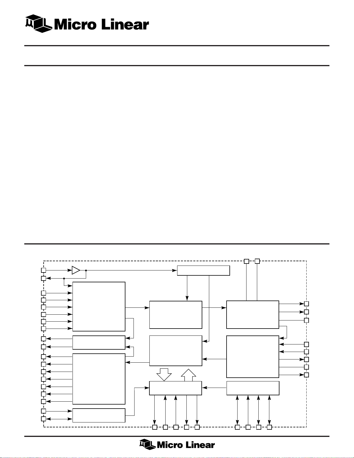
GENERAL DESCRIPTION
The ML6692 implements the complete physical layer of
the Fast Ethernet 100BASE-TX standard. The ML6692
interfaces to the controller through the standard-compliant
Media Independent Interface (MII). The ML6692
functionality includes auto-negotiation, 4B/5B encoding/
decoding, Stream Cipher scrambling/descrambling,
125MHz clock recovery/generation, receive adaptive
equalization, baseline wander correction, and MLT-3/
10BASE-T transmitter.
For applications requiring 100Mbps only, such as
repeaters, the ML6692 offers a single-chip per-port
solution. For 10/100 dual speed adapters or switchers,
10BASE-T functionality may be attained using Micro
Linear’s ML2653, or by using an Ethernet controller that
contains an integrated 10BASE-T PHY.
FEATURES
■ Single-chip 100BASE-TX physical layer
■ Compliant to IEEE 802.3u 100BASE-TX standard
■ Supports adapter, repeater and switch applications
■ Single-jack 10BASE-T/100BASE-TX solution when used
with external 10Mbps PHY
■ Compliant MII (Media Independant Interface)
■ Auto-negotiation capability
■ 4B/5B encoder/decoder
■ Stream Cipher scrambler/descrambler
■ 125MHz clock recovery/generation
■ Baseline wander correction
■ Adaptive equalization and MLT-3 encoding/decoding
■ Supports full-duplex operation
BLOCK DIAGRAM (PLCC Package)
TXCLKIN
1
TXCLK
9
TXD3
3
TXD2
4
TXD1
5
TXD0
6
TXEN
7
TXER
8
CRS
18
COL
19
RXCLK
17
RXD3
10
RXD2
12
RXD1
14
RXD0
16
RXDV
21
RXER
23
MDC
24
MDIO
25
PCS TRANSMIT
STATE MACHINE
4B/5B ENCODER
SCRAMBLER
CARRIER AND
COLLISION LOGIC
PCS RECEIVE
STATE MACHINE
5B/4B DECODER
DESCRAMBLER
MII MANAGEMENT
REGISTERS
CLOCK SYNTHESIZER
NRZ TO NRZI ENCODER
SERIALIZER
MLT-3 ENCODER
CLOCK AND DATA
RECOVERY
NRZI TO NRZ DECODER
DESERIALIZER
AUTO-NEGOTIATION
AND CONTROL LOGIC
T4EN
T4FAIL
29 30
10BTLNKEN
10BTRCV
50 51
DUPLEX
47
48
49
10BTTXINP
10BTTXINN
FLP/100BASE-TX/10BASE-T
TWISTED PAIR DRIVER
EQUALIZER
BLW CORRECTION
MLT-3 DECODER
LOOPBACK MUX
INITIALIZATION
REGISTER
EDIN
31
SEL10HD
32
33
SEL10FD
/ECLK
35
TPOUTN
LINK100
SEL100T4
/EDOUT
TPOUTP
RTSET
TPINP
TPINN
CMREF
RGMSET
40
39
37
45
44
46
36
43
1
Page 2

ML6692
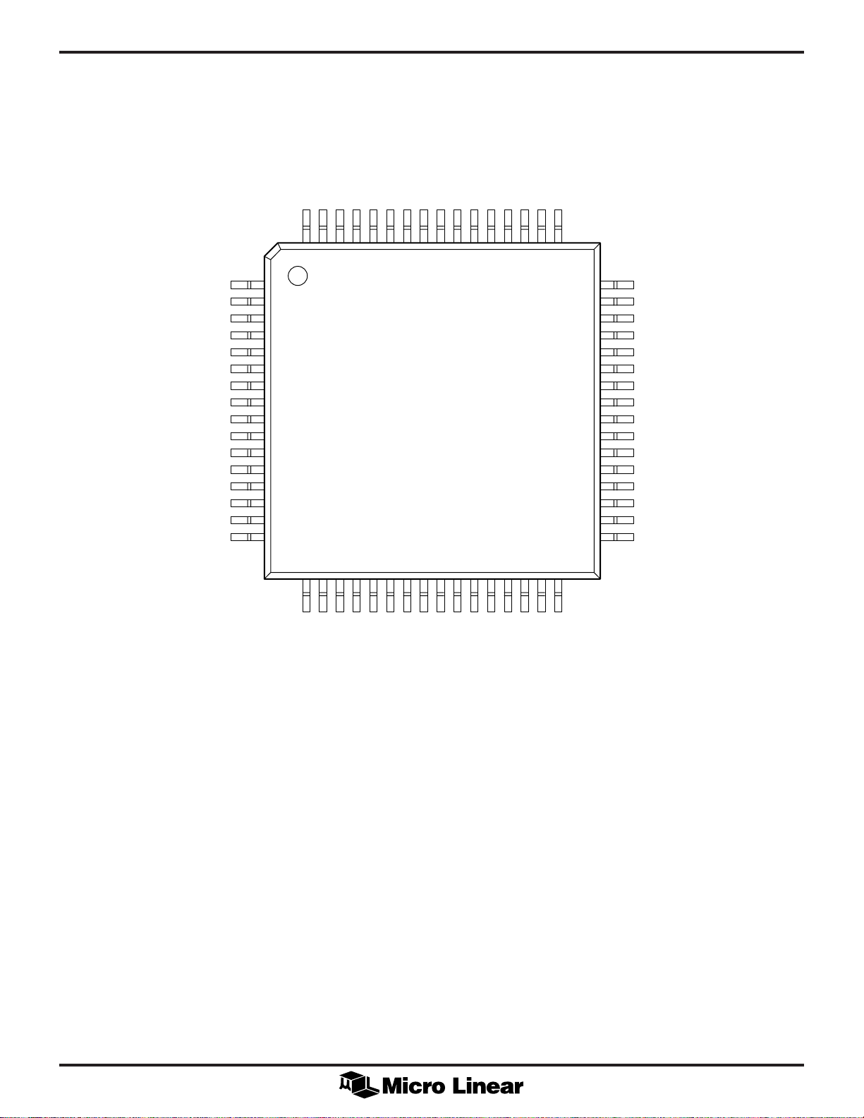
PIN CONFIGURATION
TXER
TXCLK
RXD3
DGND1
RXD2
DVCC1
RXD1
DGND2
RXD0
RXCLK
CRS
COL
DGND3
ML6692
52-Pin PLCC (Q52)
TXEN
TXD0
TXD1
TXD2
TXD3
AGND1
TXCLKIN
AVCC1
10BTLNKEN
10BTRCV
7654321525150494847
8
9
10
11
12
13
14
15
16
17
18
19
20
21 22 23 24 25 26 27 28 29 30 31 32 33
RXER
RXDV
DVCC2
MDC
MDIO
DGND4
TOP VIEW
DVCC5
T4EN
DGND5
T4FAIL
10BTTXINP
10BTTXINN
DUPLEX
46
45
44
43
42
41
40
39
38
37
36
35
34
EDIN
SEL10HD
SEL 10FD/ECLK
CMREF
TPINP
TPINN
LINK100
AVCC2
AGND2
TPOUTP
TPOUTN
AGND3
RTSET
RGMSET
SEL100T4/EDOUT
AVCC3
2
Page 3
PIN CONFIGURATION
ML6692
64-Pin TQFP (H64-10)
TXER
TXEN
TXD0
TXD1
TXD2
TXD3
AGND1A
AGND1B
TXCLKIN
AVCC1
10BTLNKEN
10TRCVNC10BTTXINP
64 63 62 61 60 595857 56 55 54 535251 50 49
10TTXINN
ML6692
NC
TXCLK
RXD3
DGND1A
DGND1B
RXD2
DVCC1A
DVCC1B
RXD1
DGND2A
DGND2B
RXD0
RXCLK
CRS
COL
DGND3A
DGND3B
1
2
3
4
5
6
7
8
9
10
11
12
13
14
15
16
17 18
19 20 21 222324 25 26 27 282930 31 32
RXER
RXDV
DVCC2
MDC
MDIO
DGND4B
DGND4A
DVCC5B
DVCC5A
DGND5B
DGND5A
T4EN
EDIN
T4FAIL
TOP VIEW
48
47
46
45
44
43
42
41
40
39
38
37
36
35
34
33
SEL10HD
SEL10FD/ECLK
DUPLEX
CMREF
TPINP
TPINN
LINK100
AVCC2
AGND2A
AGND2B
TPOUTP
TPOUTN
AGND3A
AGND3B
RTSET
RGMSET
SEL100T4/EDOUT
AVCC3
3
Page 4

ML6692
PIN DESCRIPTION (Pin Numbers for TQFP package in parentheses)
PIN NAME FUNCTION
1 (56) TXCLKIN Transmit clock TTL input. This 25MHz clock is the frequency reference for the internal
transmit PLL clock multiplier. This pin should be driven by an external 25MHz clock at
TTL or CMOS levels.
2 (57, 58) AGND1 Analog ground.
3, 4, 5, 6, TXD<3:0> Transmit data TTL inputs. TXD<3:0> inputs accept TX data from the MII. Data
(59, 60, 61, 62) appearing at TXD<3:0> are clocked into the ML6692 on the rising edge of TXCLK.
7 (63) TXEN Transmit enable TTL input. Driving this input high indicates to the ML6692 that transmit
data are present at TXD<3:0>. TXEN edges should be synchronous with TXCLK.
8 (64) TXER Transmit error TTL input. Driving this pin high with TXEN also high causes the part to
continuously transmit scrambled H symbols. When TXEN is low, TXER has no effect.
9 (1) TXCLK Transmit clock TTL output. This 25MHz clock is phase-aligned with the internal 125MHz
TX bit clock. Data appearing at TXD<3:0> are clocked into the ML6692 on the rising
edge of this clock.
10, 12, 14, 16 RXD<3:0> Receive data TTL outputs. RXD<3:0> outputs are valid on RXCLK’s rising edge.
(2, 5, 8, 11)
11 (3, 4) DGND1 Digital ground.
13 (6, 7) DVCC1 Digital +5V power supply.
15 (9, 10) DGND2 Digital ground.
17 (12) RXCLK Recovered receive clock TTL output. This 25MHz clock is phase-aligned with the
internal 125MHz bit clock recovered from the signal received at TPINP/N. Receive data
at RXD<3:0> changes on the falling edges and should be sampled on the rising edges of
this clock. RXCLK is phase aligned to TXCLKIN when the 100BASE-TX signal is not
present at TPINP/N.
18 (13) CRS Carrier Sense TTL output. For 100Mbps operation in standard mode, CRS goes high in the
presennon-idle signals at TPINP/N, or when the ML6692 is transmitting. CRS goes low when
there is no transmit activity and receive is idle. For 100 Mbps operation in repeater mode
or half duplex mode, CRS goes high in the presence of non-idle signals at TPINP/N only.
19 (14) COL Collision Detected TTL output. For 100 Mbps operation COL goes high upon detection of
a collision on the network, and remains high as long as the collision condition persists.
COL is low when the ML6692 operates in either full duplex, or loopback modes.
20 (15, 16) DGND3 Digital ground.
21 (17) RXDV Receive data valid TTL output. This output goes high when the ML6692 is receiving a
data packet. RXDV should be sampled synchronously with RXCLK’s rising edge.
22 (18) DVCC2 Digital +5V power supply.
23 (19) RXER Receive error TTL output. This output goes high to indicate error or invalid symbols
within a packet, or corrupted idle between packets. RXER should be sampled
synchronously with RXCLK’s rising edge.
24 (20) MDC MII Management Interface clock TTL input. A clock at this pin clocks serial data into or
out of the ML6692’s MII management registers through the MDIO pin. The maximum clock
frequency at MDC is 2.5MHz.
4
Page 5

ML6692
PIN DESCRIPTION (Continued)
PIN NAME FUNCTION
25 (21) MDIO MII Management Interface data TTL input/output. Serial data are written to and read
from the ML6692’s management registers through this I/O pin. Input data is sampled on the
rising edge of MDC. Data output should be sampled synchronously with MDC's rising
edge.
26 (22, 23) DGND4 Digital ground.
27 (24, 25) DVCC5 Digital +5V power supply.
28 (26, 27) DGND5 Digital ground.
29 (28) T4EN 100BASE-T4 enable TTL output. This output goes low if the auto-negotiation function
chooses 100BASE-T4 as the highest common denominator technology. This output is high
on power-up, during auto-negotiation, when the ML6692 enables any other protocol, or
when 100BASE-T4 technology is not supported. If auto-negotiation is disabled, T4EN is
always low.
30 (29) T4FAIL 100BASE-T4 link fail TTL input. When driven high, it indicates a good, 100BASE-T4 link.
When the auto-negotiation function chooses 100BASE-T4 as the highest common
denominator technology, and indicates it by driving T4EN low, T4FAIL should go high
within 750-1000ms; otherwise auto-negotiation is restarted. Driving this pin low after autonegotiation is completed, also restarts it. In the parallel detection function, driving this pin
high indicates that the 100BASE-T4 link is ready. If auto-negotiation is disabled and
management register bit 0.13 is set to 1 (100Mb/s data rate selected), driving T4FAIL
high indicates a valid 100BASE-T4 link and disables the ML6692’s 100BASE-TX analog
functions. If bit 13 of the MII Control register is set to 0, T4FAIL has no effect.
31 (30) EDIN Initialization interface mode select and EEPROM interface mode data-in CMOS
input/output. EDIN selects one of three possible interface modes at power up. See table
on page 14 for more detail
32 (31) SEL10HD Initialization Interface 10BASE-T half duplex CMOS input. When EDIN is high or
floating, this pin has no effect. When EDIN is low, this pin sets the value of bit 11 of the
MII Status register (10Mb/s half duplex), and the default value of bit 5 of the MII
Advertisment register (10BASE-T half duplex capability).
33 (32) SEL10FD/ Initialization Interface 10BASE-T full duplex CMOS input/clock CMOS input/output. ECLK
ECLK When EDIN is low, this pin sets the value of bit 12 of the MII Status register (10Mb/s full
duplex), and the default value of bit 6 of the MII Advertisement register (10BASE-T full
duplex capability). When EDIN is left floating, this pin provides the output clock to read
initialization data from an external EEPROM. When EDIN is high, this pin is the input
clock to load data from an external microcontroller.
34 (33) AVCC3 Analog +5V power supply.
35 (34) SEL100T4/ Initialization Interface 100BASE-T4 CMOS input and EEPROM or microcontroller
EDOUT data-out CMOS input. When EDIN is low, this pin sets the value of bit 15 of the MII
Status register (100BASE-T4), and the default value of bit 9 of the MII Advertisement
register (100BASE-T4 capability). When EDIN is floating, this pin is the initialization
data input from an external EEPROM. When EDIN is high, this pin is the initialization
data input from a microcontroller.
36 (35) RGMSET Equalizer bias resistor input. An external 9.53ký, 1% resistor connected between
RGMSET and AGND3 sets internal time constants controlling the receive equalizer
transfer function.
5
Page 6

ML6692
PIN DESCRIPTION (Continued)
37 (36) RTSET Transmit level bias resistor input. An external 2.49kW, 1% resistor connected between
RTSET and AGND3 sets a precision constant bias current for the twisted pair transmit
level.
38 (37, 38) AGND3 Analog ground.
39, 40 (39, 40) TPOUTN/P Transmit twisted pair outputs. This differential current output pair drives FLP waveforms
and MLT-3 waveforms into the network coupling transformer in 100BASE-TX mode, or
10BASE-T waveforms in 10BASE-T mode.
41 (41, 42) AGND2 Analog ground.
42 (43) AVCC2 Analog +5V power supply.
43 (44) LINK100 100BASE-TX link activity open-drain output. LINK100 pulls low when there is 100BASE-
TX activity at TPINP/N in 100BASE-TX or auto-negotiation modes. This output is capable
of driving an LED directly.
44, 45 (45, 46) TPINN/P Receive twisted pair inputs. This differential input pair receives 100BASE-TX, FLP, or
10BASE-T signals from the network.
46 (47) CMREF Receiver common-mode reference output. This pin provides a common-mode bias point
for the twisted-pair media line receiver, typically (VCC – 1.26)V.
47 (48) DUPLEX Full duplex enabled TTL output. This output is high during the auto-negotiation process,
it’s low when auto-negotiation is reset (power-up, reset bit, restart auto-negotiation bit,
power down bit, or link loss) and follows the duplex status otherwise. It drives the
ML2653’s FD input, and prevents the ML2653 from attempting to transmit during autonegotiation. For 10BASE-T transceivers without pin-selectable MAU loopback disable,
DUPLEX can be used to disable the 10BASE-T transceiver’s receive and collision outputs
to the controller during auto-negotiation.
48, 49 (50, 51) 10BTTXINN/P 10BASE-T transmit waveform inputs. The ML6692 presents a linear copy of the input at
10BTTXINP/N to the TPOUTP/N outputs when the ML6692 functions in 10BASE-T mode.
Signals presented to these pins must be centered at VCC/2 and have a single ended
amplitude of ±0.25V.
50 (53) 10BTRCV 10BASE-T receive activity TTL input. The external 10BASE-T transceiver drives this pin
high to indicate 10BASE-T packet reception from the network.
51 (54) 10BTLNKEN 10BASE-T link control TTL output. This output is low if the ML6692 is in 10BASE-T mode,
or if the auto-negotiation function indicates to the 10BASE-T PMA to scan for carrier. This
output is high if the 10BASE-T PMA should be disabled.
52 (55) AVCC1 Analog +5V power supply.
6
Page 7

ABSOLUTE MAXIMUM RATINGS
ML6692
Absolute maximum ratings are those values beyond which
the device could be permanently damaged. Absolute
maximum ratings are stress ratings only and functional
device operation is not implied.
Lead Temperature (Soldering, 10 sec) .....................260°C
Thermal Resistance (qJA)
PLCC ............................................................... 40°C/W
TQFP ............................................................... 52°C/W
VCC Supply Voltage Range .................. GND –0.3V to 6V
Input Voltage Range
OPERATING CONDITIONS
Digital Inputs ...................... GND – 0.3V to VCC +0.3V
TPINP, TPINN, 10BTTXNP, 10BTTXINN, .......................
........................................... GND –0.3V to VCC +0.3V
Output Current
TPOUTP, TPOUTN .............................................. 60mA
All other outputs ................................................. 10mA
Junction Temperature .............................................. 150°C
Storage Temperature .............................–65°C to +150°C
VCC Supply Voltage............................................ 5V ±5%
All VCC supply pins must be within 0.1V of each other.
All GND pins must be within 0.1V of each other.
TA , Ambient temperature.............................. 0ºC to 70°C
RGMSET .................................................... 9.53kW ± 1%
RTSET ........................................................ 2.49kW ± 1%
Receive transformer insertion loss ...................... <–0.5dB
DC ELECTRICAL CHARACTERISTICS
Over full range of operating conditions unless otherwise specified (Note 1).
SYMBOL PARAMETER CONDITIONS MIN TYP MAX UNITS
RECEIVER
V
ICM
TPINP/N Input Common-Mode VCC – 1.26 V
Voltage (CMREF)
V
R
IDR
I
ICM
I
RGM
I
LED OUTPUT (LINK100)
I
OLS
I
OHS
TRANSMITTER
I
TD100
I
TD10
I
TOFF
I
TXI
TPINP-TPINN Differential Input –3.0 3.0 V
ID
Voltage Range
TPINP-TPINN Differential 10.0k W
Input Resistance
TPINP/N Common-Mode Input Current +10 µA
RGMSET Input Current RGMSET = 9.53kW 130 µA
RTSET Input Current RTSET = 2.49kW 500 µA
RT
Output Low Current 5mA
Output Off Current 10 µA
TPOUTP/N 100BASE-TX Mode Note 2, 3 ±19 ±21 mA
Differential Output Current
TPOUTP/N 10BASE-T ±55 ±60 ±65 mA
Mode Differential Output Current
TPOUTP/N Off-State Output RL = 200, 1% 0 1.5 mA
TPOUTP/N Differential Output
Current Imbalance RL = 200, 1% 500 µA
7
Page 8

ML6692
DC ELECTRICAL CHARACTERISTICS (Continued)
SYMBOL PARAMETER CONDITIONS MIN TYP MAX UNITS
TRANSMITTER (Continuied)
X
ERR
TPOUTP/N Differential Output V
= VCC; Note 3 –5.0 +5.0 %
OUT
Current Error
X
CMP100
V
OCM10
TPOUTP/N 100BASE-X Output V
Current Compliance Error I
TPOUTP/N 10BASE-T Output I
= VCC ± 2.2V; referred to
OUT
at V
OUT
TD10
CC
remains within specified V
Voltage Compliance Range values
V
ICM10
10BTTXNN/P Input VCC/2 – 0.3 VCC/2 + 0.3 V
Common-Mode Voltage Range
POWER SUPPLY CURRENT
I
CC100
Supply Current, 100BASE-TX Current into all VCC pins 200 300 mA
Operation, Transmitting
I
CC10
Supply Current, 10BASE-T Current into all VCC pins 40 70 mA
Operation, Transmitting
I
CCOFF
Supply Current Current into all VCC pins 20 mA
Power Down Mode
I
CCAUTO
Supply Current During Current into all VCC pins 240 300 mA
Auto-negotiation
TTL INPUTS (TXD<3:0>, TXCLKIN, MDC, MDIO, TXEN, TXER, 10BTRCV, T4FAIL)
V
V
I
I
Input Low Voltage I
IL
Input High Voltage I
IH
Input Low Current V
IL
Input High Current V
IH
= –400µA 0.8 V
IL
= 100µA 2.0 V
IH
= 0.4V –200 µA
IN
= 2.7V 100 µA
IN
MII TTL OUTPUTS (RXD<3:0>, RXCLK, RXDV, RXER, CRS, COL, MDIO, TXCLK)
–2.0 +2.0 %
– 2.7 V
CC
+ 2.7 V
CC
V
V
OLT
OHT
Output Low Voltage I
Output High Voltage I
= 4mA 0.4 V
OL
= –4mA 2.4 V
OH
NON-MII TTL OUTPUTS (DUPLEX, T4EN, 10BTLNKEN)
V
V
OLT
OHT
Output Low Voltage I
Output High Voltage I
= 1mA 0.4 V
OL
= –0.1mA 2.4 V
OH
CMOS INPUTS (EDIN, SEL10HD, SEL10FD/ECLK, SEL100T4/EDOUT)
V
ILC
V
IHC
Input Low Voltage 0.2 x V
Input High Voltage 0.8 x V
CMOS OUTPUTS (SEL10FD/ECLK)
V
V
OLC
OHC
Output Low Voltage IOL = 2mA 0.1 x V
Output High Voltage IOL = –2mA 0.9 x V
CC
CC
CC
CC V
V
V
V
8
Page 9

ML6692
AC ELECTRICAL CHARACTERISTICS
Over full range of operating conditions unless otherwise specified
SYMBOL PARAMETER CONDITIONS MIN TYP MAX UNITS
RECEIVER
V
ICM
TPINP/N Input Common-Mode VCC – 1.26 V
Voltage (CMREF)
TRANSMITTER (NOTE 3)
t
TR/F
TPOUTP-TPOUTN Differential Notes 5, 6; for any legal 3.0 5.0 ns
Rise/Fall Time code sequence
t
TM
TPOUTP-TPOUTN Differential Notes 5, 6; for any legal –0.5 0.5 ns
Rise/Fall Time Mismatch code sequence
t
TDC
TPOUTP-TPOUTN Differential Notes 4, 6 –0.5 0.5 ns
Output Duty Cycle Distortion
t
TJT
TPOUTP-TPOUTN Differential Note 6 300 1400 ps
Output Peak-to-Peak Jitter
X
OST
TPOUTP-TPOUTN Differential Notes 6, 7 5 %
Output Voltage Overshoot
t
t
CLK
TXP
TXCLKIN – TXCLK Delay 6 11 ns
Transmit Bit Delay Note 8 10.5 bit times
RECEIVER
t
RXDC
t
RXDR
Receive Bit Delay (CRS) Note 9 15.5 bit times
Receive Bit Delay (RXDV) Note 10 25.5 bit times
MII (MEDIA-INDEPENDENT INTERFACE)
X
BTOL
t
TPWH
t
TPWL
t
RPWH
t
RPWL
t
TPS
t
TPH
t
RCS
t
RCH
t
RPCR
t
RPCF
TX Output Clock Frequency 25MHz frequency –100 +100 ppm
Tolerance
TXCLKIN pulse width HIGH 14 ns
TXCLKIN pulse width LOW 14 ns
RXCLK pulse width HIGH 14 ns
RXCLK pulse width LOW 14 ns
Setup time, TXD<3:0> Data 13 ns
Valid to TXCLK Rising Edge
(1.4V point)
Hold Time, TXD<3:0> Data 0 ns
Valid After TXCLK Rising Edge
(1.4V point)
Time that RXD<3:0> Data are 10 ns
Valid Before RXCLK Rising Edge
(1.4V point)
Time that RXD<3:0> Data are 10 ns
Valid After RXCLK Rising Edge
(1.4V point)
RXCLK 10% – 90% Rise Time 6ns
RXCLK 90%-10% Fall Time 6ns
9
Page 10

ML6692
AC ELECTRICAL CHARACTERISTICS
SYMBOL PARAMETER CONDITIONS MIN TYP MAX UNITS
MDC-MDIO (MII MANAGEMENT INTERFACE)
t
SPWS
Write Setup Time, MDIO Data 10 ns
Valid to MDC Rising Edge
1.4V Point
t
SPWH
Write Hold Time, MDIO Data 10 ns
Valid After MDC Rising Edge
1.4V Point
t
SPRS
Read Setup Time, MDIO Data 100 ns
Valid to MDC Rising Edge
1.4V Point
t
SPRH
Read Hold time, MDIO Data 0 ns
Valid After MDC Rising Edge
1.4V Point
t
CPER
t
CPW
Period of MDC 400 ns
Pulsewidth of MDC Positive or negative pulses 160 ns
INITIALIZATION INTERFACE
t
PW1
t
PW2
t
PER1
t
DV1
ECLK Positive Pulsewidth EDIN floating (EEPROM Mode) 900 ns
ECLK Negative Pulsewidth EDIN floating (EEPROM Mode) 900 ns
ECLK Period, EEPROM Mode EDIN floating (EEPROM Mode) 1800 ns
EDOUT Data Valid Time After EDIN floating (EEPROM Mode) 900 ns
ECLK Rising Edge
t
PER2
t
PW3
t
PW4
t
t
H1
ECLK period EDIN high (Microcontroller Mode) 5000 ns
ECLK Positive Pulsewidth EDIN high (Microcontroller Mode) 2000 ns
ECLK Negative Pulsewidth EDIN high (Microcontroller Mode) 2000 ns
ECLK Data Setup Time EDIN high (Microcontroller Mode) 10 ns
S1
ECLK Data Hold Time EDIN high (Microcontroller Mode) 10 ns
Note 1. Limits are guaranteed by 100% testing, sampling, or correlation with worst case test conditions.
Note 2. Measured using the test circuit shown in fig. 1, under the following conditions:
R
= 200W, RLS = 49.9W, R
LP
All resistors are 1% tolerance.
Note 3. Output current amplitude is I
Note 4. Measured relative to ideal negative and positive signal 50% points, using the four successive MLT-3 transitions for the 01010101 bit sequence.
Note 5. Time difference between 10% and 90% levels of the transition from the baseline voltage (nominally zero) to either the positive or negative peak signal
Note 6. Differential test load is shown in fig. 1 (see note 2).
Note 7. Defined as the percentage excursion of the differential signal transition beyond its final adjusted value during the symbol interval following the transition. The
Note 8. From first rising edge of TXCLK after TXEN goes high, to first bit of J at the MDI.
Note 9. From first bit of J at the MDI, to CRS.
Note 10. From first bit of J at the MDI, to first rising edge of RXCLK after RXDV goes high.
voltage. The times specified here correlate to the transition times defined in the ANSI X3T9.5 TP-PMD Rev 2.0 working draft, section 9.1.6, which include the
effects of the external network coupling transformer and EMI/RFI emissions filter.
adjusted value is obtained by doing a straight line best-fit to an output waveform containing 14 bit-times of no transition preceded by a transition from zero to
either a positive or negative signal peak; the adjusted value is the point at which the straight line fit meets the rising or falling signal edge.
= 2.49kW.
TSET
= 40W 1.25V/RTSET.
OUT
10
Page 11

ML6692
V
CC
TXCLKIN
TXD<3:0>
TXCLK
TXER
TXEN
TPOUTP
TPOUTN
R
200Ω
R
200Ω
LP
LP
2:1
R
50Ω
LS
Figure 1.
t
TPWH
t
TPS
t
TPH
t
TPWL
Figure 2. MII Transmit Timing
2
R
50Ω
1
LS
RXCLK
RXD<3:0>
RXER
RXDV
MDC
MDIO
MDC
t
RPCR
t
RCS
t
RCH
Figure 3. MII Receive Timing
t
SPWS
t
SPWH
Figure 4. MII Management Interface Write Timing
t
CPER
t
RPCF
MDIO
t
SPRS
SPRH
t
CPW
t
CPW
t
Figure 5. MII Management Interface Read Timing
11
Page 12

ML6692
FUNCTIONAL DESCRIPTION
TRANSMIT SECTION
100BASE-TX Operation
The transmitter includes everything necessary to accept
4-bit data nibbles clocked in at 25MHz at the MII and
output scrambled, 5-bit encoded MLT-3 signals into
twisted pair at 100Mbps. The on-chip transmit PLL
converts a 25MHz TTL-level clock at TXCLKIN to an
internal 125MHz bit clock. TXCLK from the ML6692
clocks transmit data from the MAC into the ML6692’s
TXD<3:0> input pins upon assertion of TXEN. Data from
the TXD<3:0> inputs are 5-bit encoded, scrambled, and
converted from parallel to serial form at the 125MHz
clock rate. The serial transmit data is converted to MLT-3
3-level code and driven differentially out of the TPOUTP
and TPOUTN pins at nominal ±2V levels with the proper
loads. The transmitter is designed to drive a center-tapped
transformer with a 2:1 winding ratio, so a differential 400ý
load is used on the transformer primary to properly
terminate the 100W cable and termination on the
secondary. The transformer’s center tap must be tied to
VCC. A 2:1 transformer allows using a ±20mA output
current in 100BASE-TX mode and ±60mA in fast link pulse
and 10BASE-T modes. Using a 1:1 transformer would have
required twice the output current and increased the onchip power dissipation. An external 2.49kW, 1% resistor at
the RTSET pin creates the correct output levels at
TPOUTP/N.
Driving TXER high when TXEN is high causes the H
symbol (00100) to appear in scrambled MLT-3 form at
TPOUTP/N. The media access controller asserts TXER
synchronously with TXCLK rising edge, and the H symbol
appears at least once in place of a valid symbol in the
current packet.
With no data at TXD<3:0> or with the ML6692 in isolate
mode (MII Management register bit 0.10 set to a 1),
scrambled idle appears at TPOUTP/N.
the 10BASE-T harmonic content requirements. The
ML6692 does not provide any 10BASE-T transmit filtering.
The ML2653 10BASE-T physical interface chip provides a
waveshaped 10BASE-T output and may be used with a
resistive load network for a simple 2-chip 10/100 solution
with the ML6692. The ML2653 interfaces to a controller
through it’s “7-wire” interface.
RECEIVE SECTION
100BASE-TX Operation
The receiver includes all necessary functions for
converting 3-level MLT-3 signals from the twisted-pair
media to 4-bit data nibbles at RXD<3:0> with extracted
clock at RXCLK. The adaptive equalizer compensates for
cable distortion and attenuation, corrects for DC baseline
wander, and converts the MLT-3 signal to 2-level NRZ.
The receive PLL extracts clock from the equalized signal,
providing additional jitter attenuation, and clocks the
signal through the serial to parallel converter. The
resulting 5-bit nibbles are descrambled, aligned and
decoded, and appear at RXD<3:0>. The ML6692 asserts
RXDV when it’s ready to present properly decoded
receive data at RXD<3:0>. The extracted clock appears at
RXCLK. Resistor RGMSET sets internal time constants
controlling the adaptive equalizer’s transfer function.
RGMSET must be set to 9.53kW (1%).
The receiver will assert RXER high if it detects code errors
in the receive data packet, or if the idle symbols between
packets are corrupted.
COL goes high to indicate simultaneous 100BASE-TX
receive and transmit activity (a collision). CRS goes high
whenever there is either receive or transmit activity in the
ML6692’s “station” mode (the default mode; see
Initialization Interface section below for more
information). In the ML6692’s “repeater” mode, CRS goes
high only when there is receive activity.
Auto Negotiation and Fast Link Pulses (FLPs)
During the auto negotiation process, the transmitter
produces nominal 5V fast link pulses (FLP’s) at
TPOUTP/N (2.5V after 2:1 transformer). When the auto
negotiation process is complete, the transmitter either
switches over to 100BASE-TX mode, activates the
10BTTXINP/N inputs for 10BASE-T operation with an
external 10BASE-T transceiver, or enables a 100BASE-T4
PMA and powers down the on-chip transmitter.
10BASE-T
In 10BASE-T mode, the transmitter acts as a linear buffer
with a gain of 10. 10BASE-T inputs (Manchester data and
normal link pulses) at 10BTTXINP/N appear as full-swing
signals at TPOUTP/N in this mode. Inputs to the
10BTTXINP/N pins should have a nominal ±0.25V
differential amplitude and a common-mode voltage of
VCC/2, and should also be waveshaped or filtered to meet
12
Auto Negotiation
The 100BASE-TX signal detect circuit in the adaptive
equalizer ignores fast and normal link pulses, and will not
pass them on to the rest of the receive channel. Instead,
FLPs (and NLPs) are recognized and processed by the auto
negotiation logic. When the auto negotiation process is
complete, either the adaptive EQ and the rest of the
100BASE-TX receive path remain active for 100BASE-TX
reception, all the ML6692’s receive circuitry is disabled
and the external 10BASE-T transceiver is enabled (if it
exists), or all the ML6692's 10BASE-T and 100BASE-TX
functionality is disabled and an external 100BASE-T4
PMA is enabled. In 10BASE-T or 100BASE-T4 modes, the
ML6692 RXD<3:0>, RXC, RXER, RXDV, COL and CRS MII
outputs are in high impedance state. See the next section
for more information on auto negotiation.
Proper connection of the TPIN pins, magnetics, and cable
is necessary for proper auto negotiation since the ML6692
Page 13

FUNCTIONAL DESCRIPTION (Continued)
ML6692
does not detect or correct errors in the polarity of fast or
normal link pulses.
USING THE ML6692 WITH AUTOMATIC LINK
CONFIGURATION
The ML6692 supports automated link protocol negotiation
and configuration. In the ML6692, the auto negotiation
state machine checks the receive signal and detects the
presence of link pulses in bursts or singly. The auto
negotiation state machine then updates the status register
in the management logic, and forces the receiver and
transmitter to perform the appropriate function, depending
on the remote link partner and local port capabilities.
If FLP (fast link pulse) bursts are detected, the auto
negotiation state machine disables all protocol-specific
link detection and drives the transmitter with answering
FLP bursts. The auto negotiation state machine then
enables the highest common denominator protocol
between the local port and the remote link partner.
If the highest common denominator technology is
100BASE-TX, the ML6692 100BASE-TX receiver is
enabled. If the highest common denominator technology
is 10BASE-T, the auto negotiation state machine disables
the ML6692 100BASE-TX receiver and enables 10BASE-T
output from the ML6692’s transmitter. If the highest
common denominator technology is 100BASE-T4, the
ML6692’s transmitter and receiver are disabled and the
external 100BASE-T4 transceiver is enabled.
The ML6692 supports the parallel detection function by
checking simultaneously for normal or fast link pulses,
100BASE-TX signal activity at TPINP/N, or indication of
100BASE-T4 activity from the external 100BASE-T4
transceiver. If one of the locally supported protocols is
detected, that protocol is enabled and all others are
disabled. If the local port lacks 10BASE-T capability and
NLPs are detected, the local auto negotiation state
machine disables transmission of all link pulses to force
the far-end station into link fail, and restarts autonegotiation.
With MII Management register bit 0.12 = 0 (auto
negotiation disabled) the ML6692 can be forced into a
certain mode using bits 0.13 (speed select), bit 0.8
(duplex mode), and pin T4FAIL, as shown in the following
table.
SPEED DUPLEX T4FAIL MODE
SELECT MODE
1 1 0 100BASE-TX Full Duplex
1 0 0 100BASE-TX Half Duplex
1 X 1 100BASE-T4
0 1 X 10BASE-T Full Duplex
0 0 X 10BASE-T Half Duplex
ML6692 PHY MANAGEMENT FUNCTIONS
The ML6692 has management functions controlled by the
register locations given in Tables 2–6. There are five 16-bit
MII Management registers, with several unused locations.
Unused locations are generally reserved for future use.
Register 0 (Table 2) is the basic control register (read/
write). Register 1 (Table 3) is the basic status register
(read-only). Register 4 (Table 4) is the auto-negotiation
capability advertisement register. Register 5 (Table 5) is
the auto-negotiation link partner ability register (what the
far-end station is capable of; read-only). Register 6 (Table
6) is the auto-negotiation expansion register (indicates
some additional auto-negotiation status information; readonly). Note that status bits 1.11-1.12 (10BASE-T
capability) and 1.15 (100BASE-T4) depend on the values
programmed through the Initialization Interface. See the
initialization interface section for programming
information. The ML6692 powers on with all management
register bits set to their default values.
The ML6692’s auto negotiation status and control register
addresses and functions match those described for the MII
in IEEE 802.3u section 22. IEEE 802.3u specifies the
management data frame structure in section 22.2.4.4.
The ML6692 takes a number of specific actions depending
on which supported technology is selected. If the
100BASE-TX technology is selected, the ML6692 switches
its clock recovery circuit from tracking the local 125MHz
bit clock to tracking the equalized, decoded receive
signal, descrambles, decodes and finds the packet
boundaries of the signal, asserts RXDV, and presents the
decoded receive data nibbles at RXD<3:0>. The ML6692
will also drive 10BTLNKEN and T4EN high to deactivate
external 10BASE-T and 100BASE-T4 transceivers. If the
100BASE-T4 transceiver detects activity, it will drive the
ML6692’s T4FAIL pin high and the ML6692 will place its
receiver and transmitter in an idle state, and will drive
10BTLNKEN high.
See the IEEE 802.3u Specification section 28 for auto
negotiation state machine definition, FLP timing, and
overall operation.
See IEEE 802.3u section 22.2.4 for a discussion of MII
management functions and status/control register
definitions.
13
Page 14

ML6692
INITIALIZATION INTERFACE
The ML6692 has an Initialization Interface to allow
register programming that is not supported by the MII
first. Therefore, the data pattern must be reversed before
programming it into the EEPROM.
Management Interface. The intitialization data is loaded
at power-up and cannot be changed afterwards. The pin
MICROCONTROLLER PROGRAMMING
EDIN selects one of three possible programming modes.
The Initialization Register bit assignment is shown in
Table 1.
With EDIN high, the ML6692 expects the 16
configuration bits transfered directly at EDOUT,
synchronized with the first 16 clock rising edges provided
EEPROM PROGRAMMING
externally at ECLK after power-up. This mode is useful
with a small microcontroller; one controller can program
With EDIN floating (set to a high impedance), the
ML6692 reads the 16 configuration bits from an external
several ML6692 parts by selectively toggling their ECLK
pins. Interface timing is shown in Figure 7.
serial EEPROM (93LC46 or similar) using the industrystandard 3-wire serial I/O protocol. After power up, the
ML6692 HARD-WIRED DEFAULT
ML6692 automatically generates the address at EDIN and
the clock at ECLK to read out the 16 configuration bits.
The EEPROM generates the configuration bit stream at
EDOUT, synchronized with ECLK. Interface timing is
shown in Figure 6. It is important to note that the ML6692
With EDIN low, the SEL10HD, SEL10FD, and SEL100T4
pins set their corresponding bits in the management status
register, and the ML6692 responds to MII PHYAD 00000
only.
expects LSBs first, whereas the 93LC46 shifts MSBs out
FUNCTION OF RELATED PINS
EDIN MODE SEL10FD/ECLK SEL100T4/EDOUT SEL10HD
Floating EEPROM ECLK (Output Clock EDOUT (Input Data No Affect
(EEPROM ADDR) to EEPROM) from EEPROM)
High Microcontroller ECLK (Input Clock EDOUT (Input Data No Affect
from Microcontroller) from Microcontroller)
Low Hardwired SEL10FD SEL100T4 SEL10HD
(Initialization bit 9) (Initialization bit 8) (Initialization bit 10)
ECLK
(DRIVEN BY
ML6692)
EDIN
(DRIVEN BY
ML6692)
EDOUT
(DRIVEN BY
EEPROM)
t
PW1
01
02 03 04 05 06 07 08 09 10 11
SB1OP11OP00A50A40A30A20A10A0
t
PW2
Figure 6. EEPROM Interface Timing
t
PW3
ECLK
(INPUT TO
ML6692)
EDOUT
(INPUT TO
ML6692)
01 02 16
t
H1
t
S1
Figure 7. Microcontroller Mode Interface Timing
t
PER1
12 13 26
0
D0 D1 D2 D3 D14 D15
t
DV1
16 BITS DATA ADDRESS
t
PER2
t
PW4
14
Page 15

ML6692
INITIALIZATION INTERFACE REGISTER
BIT(S) NAME DESCRIPTION R/W DEFAULT
I.15 PHY A4 PHY address bit 4 0
I.14 PHY A3 PHY address bit 3 0
I.13 PHY A2 PHY address bit 2 0
I.12 PHY A1 PHY address bit 1 0
I.11 PHY A0 PHY address bit 0 0
I.10 10HDUP 10BASE-T half duplex initialization bit 0
1 = 10BASE-T (half-duplex) capability
0 = no 10BASE-T (half-duplex) capability
I.9 10FDUP 10BASE-T full duplex initialization bit 0
1 = 10Mb/s full duplex capability
0 = no 10Mb/s full duplex capability
I.8 100T4 100BASE-T4 initialization bit 0
1 = 100BASE-T4 capability
0 = no 100BASE-T4 capability
I.7 ISODIS Isolate bit disable (bit 0.10) 0
I.6 REPEATER Repeater mode: when this bit is set to 1, 0
CRS isonly asserted when receiving non-idle
signal at TPINP/N, and the ML6692 is
forced to half duplex mode
I.5–I.0 Not used
Note: Bits I<10:8> are the values for bits 1.11, 1.12 and 1.15 and initial values for bits 4.5, 4.6 and 4.9 of the MII Management Interface.
Table 1. Initialization Interface Register
MII MANAGEMENT INTERFACE REGISTERS
BIT(S) NAME DESCRIPTION R/W DEFAULT
0.15 Reset 1 = reset all register bits to defaults R/W, SC 0
0 = normal operation
0.14 Loopback 1 = PMD loopback mode R/W 0
0 = normal operation
0.13 Manual speed select 1 = 100Mb/s R/W 1
(Active when 0.12 = 0) 0 = 10Mb/s
0.12 Auto negotiation enable 1 = enable auto negotiation R/W 1
0 = disable auto negotiation
0.11 Power down 1 = power down R/W 0
0 = normal operation
0.10 Isolate 1 = electrically isolate the ML6692 from MII R/W 1
0 = normal operation
0.9 Restart auto negotiation 1 = restart auto negotiation R/W, SC 0
0 = normal operation
0.8 Duplex mode 1 = Full duplex select, auto negotiation disabled R/W 0
0 = Half duplex select, auto negotiation disabled
0.7 Collision Test 1 = enable COL signal test R/W 0
0 = normal operation
0.6 – 0.0 Not Used
Table 2. Control Register
15
Page 16

ML6692
MII MANAGEMENT INTERFACE REGISTERS (Continuied)
BIT(S) NAME DESCRIPTION R/W DEFAULT
1.15 100BASE-T4 1 = 100BASE-T4 capability RO 100T4 (bit I.8)
0 = no 100BASE-T4 capability
1.14 100BASE-TX full duplex 1 = full duplex 100BASE-TX capability RO 1
0 = No full duplex 100BASE-TX capability
1.13 100BASE-TX half duplex 1 = half duplex 100BASE-TX capability RO 1
0 = no half duplex 100BASE-TX capability
1.12 10Mb/s full duplex 1 = full duplex 10Mb/s capability RO 10FDUP (Bit I.9)
0 = No full duplex 10Mb/s capability
1.11 10BASE-T (half duplex) 1 = 10BASE-T (half duplex) capability RO 10HDUP (Bit I.10)
0 = No 10BASE-T (half duplex) capability
1.10 – 1.6 Not Used
1.5 Auto negotiation compl. 1 = auto negotiation process complete RO 0
0 = auto negotiation not complete
1.4 Not Used
1.3 Auto negotiation ability 1 = auto negotiation capability available RO 1
0 = auto negotiation capability not available
1.2 Link status 1 = one and only one PHY-specific link is up RO/LL latch low after
0 = link is down link fail until read
1.1 Not Used
1.0 Extended capability 1 = extended register capabilities RO 1
0 = basic register set only
Table 3. Status Register
BIT(S) NAME DESCRIPTION R/W DEFAULT
4.15 Next Page 1 = additional link code word pages RO 0
0 = no additional pages
4.14 Reserved Write as zero, ignore on read RO
4.13 Remote fault 1 = remote wire fault detected R/W 0
0 = no remote wire fault detected
4.12-4.10 Reserved
4.9 100BASE-T4 capability 1 = 100BASE-T4 capability R/W 100T4 (Bit I.8)
4.8 100BASE-TX full duplex 1 = 100BASE-TX full duplex capability R/W 1
4.7 100BASE-TX 1 = 100BASE-TX capability R/W 1
4.6 10BASE-T full duplex 1 = 10BASE-T full duplex capability R/W 10FDUP (Bit I.9)
4.5 10BASE-T 1 = 10BASE-T capability R/W 10HDUP (Bit I.10)
4.4-4.1 Selector field All these bits are 0 for 802.3 LANs RO 0
4.0 Selector field This bit is a 1 for 802.3 LANs RO 1
(Not used at present)
0 = no 100BASE-T4 capability
0 = no 100BASE-Tfull duplex
0 = no 100BASE-TX capability
0 = no 10BASE-T full duplex capability
0 = no 10BASE-T capability
16
Table 4. Advertisement Register
Page 17

ML6692
MII MANAGEMENT INTERFACE REGISTERS (Continuied)
BIT(S) NAME DESCRIPTION R/W DEFAULT
5.15 Next Page 1 = additional link code word pages RO X
0 = no additional pages
5.14 Acknowledge 1 = link partner's successful receipt of local RO X
station code
0 = no link partner reception of local station
code
5.13 Remote fault 1 = remote wire fault detected R/W X
0 = no remote wire fault detected
5.12-5.10 Reserved
5.9 100BASE-T4 capability 1 = 100BASE-T4 capability R/W X
5.8 100BASE-TX full duplex 1 = 100BASE-TX full duplex capability R/W X
5.7 100BASE-TX 1 = 100BASE-TX capability R/W X
5.6 10BASE-T full duplex 1 = 10BASE-T full duplex capability R/W X
5.5 10BASE-T 1 = 10BASE-T capability R/W X
5.4-5.1 Selector field All these bits are 0 for 802.3 LANs RO X
5.0 Selector field This bit is a 1 for 802.3 LANs RO X
(Not used at present) X
0 = no 100BASE-T4 capability
0 = no 100BASE-TX full duplex
0 = no 100BASE-TX capability
0 = no 10BASE-T full duplex capability
0 = no 10BASE-T capability
Table 5. Link Partner Register
BIT(S) NAME DESCRIPTION R/W DEFAULT
6.15-6.5 Reserved; not used 0
6.4 Multiple link fault 1 = more than one receiving protocol RO; reset 0
indicates link OK on read
0 = no multiple link faults
6.3 Link partner next page able 1 = link partner supports next page RO 0
0 = link partner has no next page
6.2 Next page able 1 = local port supports next page RO 0
0 = local port has no next page
6.1 Page received 1 = 3 identical, consecutive link code RO; reset 0
words received on read
0 = 3 identical, consecutive link code
words NOT received
6.0 Link partner auto neg. capable 1 = link partner has auto negotiation capability RO 0
0 = link partner has NO auto negotiation capability
NOTE: All unnamed or unused register locations will return 0 values when accessed.
KEY: LL = latch low until read, R/W = read/write, RO = read only, SC = self-clearing.
Table 6. Expansion Register
17
Page 18

ML6692
AVCC
FB1
DVCC
D3
D2
D5
8
10 9
14 13 12 11
4321
R25
R24
C13
R13
567
U6
1234
U4
5678
C5
++
RJ45
8
R11
4342414039
TPINN
LINK100
RXD3
DGND1
101112
SHIELD
GROUNDED
R17
R18
R19
AVCC2
2:1
L1
R8
AGND2
R22
TPOUTP
L2
R9
TPOUTN
R16 R15
U1
ML6692
RXD2
DVCC1
RXD1
DGND2
13141516171819
R20
R21
C2
U5
C8
R1
R2
3837363534
RTSET
AGND3
RGMSET
SEL100T4/EDOUT
RXD0
RXCLK
CRS
COL
20
AVCC3
DGND3
C14
R14
D6
ECLK
SEL10FD/
SEL10HD
EDIN
31 32 33
T4FAIL
30
T4EN
29
DGND5
28
DVCC5
DGND4
26 27
MDIO
MDC
RXER
DVCC2
RXDV
21 22 23 24 25
NC
D4
TXTP+
TXTP–
RXTP+
AVCC1
AGND1
TXD3
TXD2
TXD1
TXD0
TXEN
R10
C1
464544
DUPLEX
CMREF
10BTTXINN
10BTTXINP
10BTRCV
10BTLINKEN
TXCLKIN
TXER
8
RXTP–
C7
TPINP
TXCLK
9
1234567
C4 C11 C12
FB2
1:1
C3 C9 C10 C6
R26
C15
R3
R6
23.7Ω
R23
75Ω
R4
34Ω
4
3
U2
1
2
NC
R5
34Ω
D1
49 48 47
50
51
52
21
76543
18
18 17 16 15 14 13 12
VCC
VCC
FD
LTP
RPOL
COL
CS0
R12
11
10
9
8
7
6
5
NC
RX–
RX+
LPBK
CLK
NC
TX–
GND
GND
U3
ML2653
CS1
CS2
RXE
RXC
RXD
XMT/RCV
19
20
21
22
23
COL
RXE
RXC
RXD
RSL
24
25
NC
NC
TX+
TXC
TXD
TXE
RTX
X1
26 27 28 1 2 3 4
Table 8. 10/100 BASE-T Application Circuit
TXE
TXD
TXC
LPBK
R7
40.2kΩ
CRS
COL
TXD3
TXD2
TXD1
TXD0
TXEN
TXCLK
TXER
RXER
RXCLK
RXDV
RXD0
RXD1
RXD2
RXD3
MDC
MII INTERFACE 7-WIRE INTERFACE
MDIO
Page 19

ML6692 SCHEMATIC
ML6692
Figure 8 shows a general 10BASE-T and 100BASE-TX
design using the ML2653 (10BASE-T PHY) and ML6692
(100BASE-TX PHY).
The inductors L1 and L2 are for the purpose of improving
return loss. Capacitor C7 is recommended. It decouples
some noise at the inputs of the ML6692, and improves the
Bit Error Rate (BER) performance of the board. We
recommend having a 0.1µF Cap on every VCC pin as
indicated by C3, 4, 9-12. Also, we recommend splitting
the AVCC, AGND and DGND. It is recommended that
AGND and DGND planes are large enough for low
inductance. If splitting the two grounds and keeping the
ground planes large enough is not possible due to board
space, you could join them into one larger ground plane.
ML6692 PARTS LIST
COMPONENT DESCRIPTION
U1 ML6692 52-Pin PLCC surface mount
U2 Can Crystal Oscillator, 25MHz 4-pin surface mount
U3 ML2653 28-pin PLCC surface mount
U4 93LC46 8-pin PLCC surface mount EEPROM
U5 BEL Transformer Module 5558-1287-02, or XFMRS Inc.
XF6692TX, or Valor ST6129 (not pin compatible)
U6 HEX Inverter 74HC04
X1 20MHz XTAL surface mount
FB1, FB2 Fair-Rite SM Bead P/N 2775019447
L1, L2 130nH inductors rated at 50MHz
R1 2.49kW 1% 1/8W surface mount
R2 9.53kW 1% 1/8W surface mount
R3, R12, R24, R25 750W 5% 1/8W surface mount
R4, R5* 34.0W 1% 1/8W surface mount
R6 23.7W 1% 1/4W surface mount
R7 40.2kW 1% 1/8W surface mount
R8, R9, R26 200W 1% 1/8W surface mount
R10, R11 100W 1% 1/8W surface mount
R13, R14 100kW 10% 1/8W surface mount
R15–R20 49.9W 5% 1/8W surface mount
R21, R22 75W 5% 1/8W surface mount
R23 75W 1% 1/4W surface mount
C1, C3, C4, 0.1µF Ceramic Chip Cap
C8-12, C15 0.01µF Ceramic Chip Cap
C5, C6 10µF Tantalum Cap.
C7 10pF Cap
C2 Board layer Cap (2V rated)
C13, C14 22nF Cap
D1-D4 LED Diodes
Refer to ML2653 data sheet for CS2, CS1, and CS0 configuration
* These resistors need to be tuned to provide a 500mV
amplitude single ended signal to the ML6692 inputs.
P-P
19
Page 20

ML6692
PHYSICAL DIMENSIONS inches (millimeters)
Package: Q52
52-Pin PLCC
0.785 - 0.795
(19.94 - 20.19)
0.750 - 0.754
(19.05 - 19.15)
1
0.042 - 0.056
(1.07 - 1.42)
0.025 - 0.045
(0.63 - 1.14)
(RADIUS)
0.042 - 0.048
(1.07 - 1.22)
14
0.050 BSC
(1.27 BSC)
0.013 - 0.021
(0.33 - 0.53)
PIN 1 ID
27
0.026 - 0.032
(0.66 - 0.81)
0.472 BSC
(12.00 BSC)
0.394 BSC
(10.00 BSC)
0.750 - 0.754
40
(19.05 - 19.15)
0.165 - 0.180
(4.06 - 4.57)
SEATING PLANE
0.148 - 0.156
(3.76 - 3.96)
Package: H64-10
64-Pin (10 x 10 x 1mm) TQFP
49
0.785 - 0.795
(19.94 - 20.19)
0.009 - 0.011
(0.23 - 0.28)
0º - 8º
0.100 - 0.110
(2.54 - 2.79)
0.600 BSC
(15.24 BSC)
0.003 - 0.008
(0.09 - 0.20)
0.690 - 0.730
(17.53 - 18.54)
20
1
17
0.020 BSC
(0.50 BSC)
PIN 1 ID
0.007 - 0.011
(0.17 - 0.27)
0.394 BSC
(10.00 BSC)
33
0.472 BSC
(12.00 BSC)
0.048 MAX
(1.20 MAX)
0.037 - 0.041
(0.95 - 1.05)
0.018 - 0.030
(0.45 - 0.75)
SEATING PLANE
Page 21

PHYSICAL DIMENSIONS inches (millimeters)
ORDERING INFORMATION
PART NUMBER TEMPERATURE RANGE PACKAGE
ML6692CH 0°C - 70°C 64 Pin Thin Quad Flat Pack (TQFP)
ML6692CQ 0°C - 70°C 52 Pin Plastic Leaded Chip Carrier (PLCC)
ML6692
Micro Linear makes no representations or warranties with respect to the accuracy, utility, or completeness of the contents
of this publication and reserves the right to make changes to specifications and product descriptions at any time without
notice. No license, express or implied, by estoppel or otherwise, to any patents or other intellectual property rights is granted
by this document. The circuits contained in this document are offered as possible applications only. Particular uses or
applications may invalidate some of the specifications and/or product descriptions contained herein. The customer is urged
to perform its own engineering review before deciding on a particular application. Micro Linear assumes no liability
whatsoever, and disclaims any express or implied warranty, relating to sale and/or use of Micro Linear products including
liability or warranties relating to merchantability, fitness for a particular purpose, or infringement of any intellectual property
right. Micro Linear products are not designed for use in medical, life saving, or life sustaining applications.
© Micro Linear 2000. is a registered trademark of Micro Linear Corporation. All other trademarks are the
property of their respective owners.
Products described herein may be covered by one or more of the following U.S. patents: 4,897,611; 4,964,026; 5,027,116;
5,281,862; 5,283,483; 5,418,502; 5,508,570; 5,510,727; 5,523,940; 5,546,017; 5,559,470; 5,565,761; 5,592,128; 5,594,376;
5,652,479; 5,661,427; 5,663,874; 5,672,959; 5,689,167; 5,714,897; 5,717,798; 5,742,151; 5,747,977; 5,754,012; 5,757,174;
5,767,653; 5,777,514; 5,793,168; 5,798,635; 5,804,950; 5,808,455; 5,811,999; 5,818,207; 5,818,669; 5,825,165; 5,825,223;
5,838,723; 5.844,378; 5,844,941. Japan: 2,598,946; 2,619,299; 2,704,176; 2,821,714. Other patents are pending.
2092 Concourse Drive
San Jose, CA 95131
Tel: (408) 433-5200
Fax: (408) 432-0295
www.microlinear.com
DS6692-02
21
 Loading...