

Page 1
July 1999
ML6674
ATM 155Mbps UTP Transceiver
GENERAL DESCRIPTION
The ML6674 is a complete monolithic transceiver for
155Mbps NRZ encoded data transmission over category
5 unshielded twisted pair (UTP) and shielded twisted pair
(STP) cables. The ML6674 is compliant with the ATM
155Mbps Twisted Pair Specification. The ML6674 includes
the baseline restoration function and adaptive
equalization which will accurately compensate for line
losses exceeding 100m of UTP.
The ML6674 receive section consists of an equalizing
filter with a feedback loop for controlling effective line
compensation. The feedback loop contains a filter and
detection block for determining the proper control signal.
An ECL 100K compatible buffer at the output interfaces
directly with ATM physical interface chips.
The ML6674 transmit section accepts ECL 100K
compatible NRZ inputs.
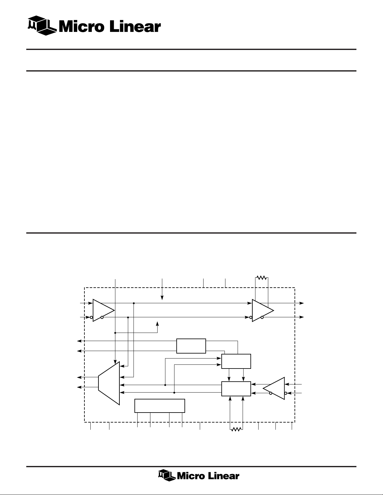
BLOCK DIAGRAM
FEATURES
■ Complies with ATM F orum 155Mbps twisted pair
specification
■ Integrated baseline wander correction circuit
■ Integrated adaptive equalization
■ Transmitter can be externally turned off
(high impedence) for true quiet line
■ Operates over 100 meters of STP or category 5 UTP
Twisted Pair Cable
■ 32-pin PLCC and TQFP
TXIN+
TXIN–
SD+
SD–
RXOUT+
RXOUT–
LPBK TXOFF TVCCA TVCCD
LINK
STATUS
MUX
ADAPTIVE
CONTROL REFERENCE
RGNDTGNDDTGNDA
RTSET1 RTSET2
ADAPTIVE
CONTROL
ADAPTIVE
EQUALIZER
RRSET2RRSET1
RTSET
TPOUT+
TPOUT–
TPIN+
TPIN–
CMREFRVCCDRVCCARRSET
1
Page 2
ML6674
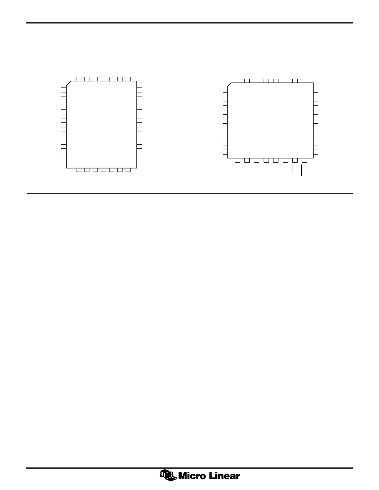
PIN CONFIGURATION
ML6674
32-Pin PCC (Q32)
RXOUT–
RVCCA
N/C
4 3 2 1 32 31 30
RXOUT+
RVCCD
TGNDD
TXOFF
SD–
SD+
N/C
LPBK
N/C
5
6
7
8
9
10
11
12
13
14 15 16 17 18 19 20
TXIN–
TXIN+
TVCCD
PIN DESCRIPTION
NAME FUNCTION
N/C
RTSET1
RTSET2
CMREF
TPOUT+
TPIN+
TPIN–
29
28
27
26
25
24
23
22
21
TPOUT–
RRSET1
RRSET2
N/C
N/C
RGND
N/C
N/C
TVCCA
TGNDA
ML6674
32-Pin TQFP (H32-7)
RRSET2
N/C
N/C
RGND
N/C
RRSET1
TPIN–
TPIN+
CMREF
N/C
N/C
RVCCA
RXOUT–
NAME FUNCTION
32 31 30 29 28 27 26 25
1
2
3
4
5
6
7
8
9 10111213141516
RVCCD
RXOUT+
SD–
SD+
N/C
N/C
TVCCA
LPBK
TGNDD
TGNDA
24
23
22
21
20
19
18
17
TXOFF
TPOUT–
TPOUT+
RTSET2
RTSET1
TVCCD
TXIN–
TXIN+
N/C
TXIN+, TXIN– These differential ECL100K compatible
inputs receive NRZ data from the PHY
for transmission.
TPOUT+, Outputs from the NRZ buffer drive
TPOUT– these differential current outputs. The
transmitter filter/transformer module
connects the media to these pins.
LPBK This TTL input enables transmitter-
Receiver loopback internally when
asserted low.
TXOFF This TTL input forces the NRZ driv er to
a high impedence state when asserted
low and shuts off transmit bias currrent.
RTSET1, An external 1% resistor connected
RTSET2 between these pins controls the
transmitter output current amplitude.
I
= 32 x 1.25V/RTSET
OUT
TVCCA, Separate analog and digital
TVCCD transmitter power supply pins help to
isolate sensitive circuitry from noise
generating digital functions. Both
supplies are nominally +5 volts.
TGNDA, Analog and digital transmitter grounds
TGNDD provide separate return paths for clean
and noisy signals.
SD+, SD– These differential ECL100K
compatible outputs indicate the
presence of a data signal with an
amplitude exceeding a preset
threshold.
TPIN+, TPIN– NRZ encoded data from the
receiver filter/transformer module
enters the Receiver through these
pins.
RXOUT+, Differential ECL100K compatible
RXOUT– outputs provide NRZ encoded data
to the PHY.
RRSET1, Internal time constants controlling
RRSET2 the equalizer’s transfer function
are set by an external resistor
connected across these pins.
CMREF This pin provides a DC common
mode reference point for the
receiver inputs.
RVCCA, Analog and digital supply pins are
RVCCD separated to isolate clean and
noisy circuit functions. Both
supplies are nominally +5 volts.
RGND Receiver ground.
2
Page 3

ML6674
ABSOLUTE MAXIMUM RATINGS
Storage T emperature................................ –65°C to 150°C
Lead Temperature (Soldering, 10 sec) .....................260°C
Absolute maximum ratings are limits beyond which the
life of the integrated circuit may be impaired. All
voltages unless otherwise specified are measured with
respect to ground.
VCC Supply Voltage Range .................. GND –0.3V to 6V
Input V oltage Range
Digital Inputs..................... GND –0.3V to VCC + 0.3V
Output Current
TPOUT+/TPOUT–, SD±, RXOUT± ......................50mA
All other outputs .................................................10mA
Junction T emperature..............................................150°C
Thermal Resistance (qJA)
PLCC ............................................................... 60°C/W
TQFP ............................................................... 80°C/W
OPERATING CONDITIONS
VCC Supply Voltage.......................................... 5V ± 5%
TA, Ambient Temperature............................... 0°C to 70°C
RTSET ............................................................. 2kW ± 1%
RRSET ........................................................ 9.53kW ± 1%
Receive transformer insertion loss ..................... < –0.5dB
ELECTRICAL CHARACTERISTICS
Unless otherwise specified, TA = T
PARAMETER CONDITIONS MIN TYP MAX UNITS
DC Characteristics
Supply Current
RVCCD 74 mA
RVCCA 65 mA
TVCCD 14 mA
TVCCA 6mA
RVCCD + RVCCA + TVCCD + TVCCA 185 mA
TTL Inputs (TXOFF, LPBK)
VIL Input Low Voltage 0.8 V
VIH Input High Voltage 2.0 V
Differential Inputs (TPIN±, TXIN±)
TPIN+, TPIN–
Common Mode Input Voltage 2.2 V
TPIN+, TPIN–
Differential Input Voltage 1.5 V
TPIN+, TPIN–
Differential Input Resistance 10 kW
TPIN+, TPIN–
Common Mode Input Current +10 µA
TXIN+, TXIN–
Input Voltage HIGH (VIH)V
TXIN+, TXIN–
Input Voltage LOW (VIL)V
TXIN+, TXIN–
Input Current LOW (IIL) 0.5 µA
TXIN+, TXIN–
Input Current HIGH (IIH) 50 µA
Differential Outputs (SD±, RXOUT±, TPOUT±)
SD+, SD–, RXOUT+, RXOUT–
Output Voltage HIGH (VOH) Note 3 VCC–1.025 VCC–0.88 V
SD+, SD–, RXOUT+, RXOUT–
Output Voltage LOW (VOL) Note 3 VCC–1.81 VCC–1.62 V
TPOUT+, TPOUT–
Differential Output Current HIGH V
MIN
to T
, VCC = 5V ±5%, RTSET = 2.0ký. (Note 1)
MAX
–1.165 VCC–0.88 V
CC
–1.810 VCC–1.475 V
CC
= VCC ± 0.5, Note 2 19.0 21.0 mA
OUT
CC
V
3
Page 4

ML6674
ELECTRICAL CHARACTERISTICS
(CONTINUED)
PARAMETER CONDITIONS MIN TYP MAX UNITS
Differential Outputs (SD±, RXOUT±, TPOUT±) (Continued)
TPOUT+, TPOUT–
DifferentialOutput Current LOW V
= VCC ± 0.5, Note 2 0 0.1 mA
OUT
TPOUT+, TPOUT–
Output Current Offset 0.5 mA
TPOUT+, TPOUT–V
OUT
= V
CC
Output Amplitude Error Note 2 –5.0 5.0 %
TPOUT+, TPOUT–V
= VCC ±1.1V
OUT
Output Voltage Compliance –2.0 +2.0 %
AC Characteristics
TPOUT+, TPOUT–
Rise/Fall Time 1.5 2.0 2.5 n s
TPOUT+, TPOUT–
Output Jitter 0.5 ns
RXOUT+, RXOUT–
Rise/Fall Time 5ns
RXOUT+, RXOUT–
Output Jitter 2.0 ns
Note 1. Limits are guaranteed by 100% testing, sampling, or correlation with worst-case test conditions.
Note 2. Output current amplitude is determined by I
Note 3. Output voltage levels are specified when terminated by 50W to V
= 32 x 1.25V/RTSET.
OUT
-2V or equivalent load.
CC
4
Page 5

FUNCTIONAL DESCRIPTION
ML6674
The ML6674 transceiver is a physical media dependent
transceiver that allows the transmission and reception of
155 Mbps data over 100 meters over shielded twisted pair
cable or category 5 unshielded twisted pair cable.
The transmit section accepts NRZ data, sending the
information on a two pin current driven tr ansmitter. Th e
transmitted output passes through an external low pass
filter and transformer before entering the connectors to the
STP or UTP cable. The output amplitude of the transmitted
signal is programmable through the external RTSET
resistor.
The receive section accepts NRZ coded data after it
passes through an isolation transformer and band limiting
filter. The adaptive equalizer is used to compensate for
the amplitude and phase distortion incurred from the
cable. The adaptive control section determines the signal
amplitude (and therefore the cable length) and adjusts the
equalizer accordingly. As the input signal amplitude
diminishes, the amount of equalization increases until it
reaches its maximum (Figure 1).
The receiver also includes the Baseline Wander correction
circuitry. The circuit will compensate and track the DC
baseline wander caused by DC imbalance of the received
data. A 10pF capacitor can be connected between TPIN+
and TPIN– to improve Bit Error Rate.
The adaptive control block governs both the equalization
level as well as the signal detection status. Signal detect
is asserted when the equalizer control loop settles, or
when loop back is asserted. When the input signal is
small, the equalization will be at its maximum.
After the signal has been equalized, it is fed through the
loopback multiplexer onto the RXOUT± pins.
Figure 1 shows a typical gain vs frequency plot of the
adaptive equalizer for 0, 25, 50, 75 and 100 meter
category 5 cable lengths.
TRANSMISSION
PECL level scrambled NRZ data is received by the
ML6674 and the current driven transmitter then sent the
data to the filter/transformer module. The transmit
amplitude is controlled by one external resistor, RTSET.
=
×32 125.
RTSET
I
OUT
V
For ATM UTP applications the transmit amplitude is 1V
peak to peak. The termination at the transmitter output is
50ý. Therefore the transmit current I
= 1/50 = 20 mA.
OUT
Thus,
V
×
32 125
RTSET
20
.
mA
k=
=Ω
2
The transmitter may be disabled via the TXOFF pin. When
this pin is pulled low, the transmitter’s output goes to a
high impedance state and no current flows through the
transformer.
ADAPTIVE EQUALIZATION
During transmission of data over UTP (unshielded twisted
pair), distortion and ISI are caused by dispersion in the
cable. Equalization is used to overcome this signal
corruption. However, the distortion is frequency
dependent and cable length dependent. Therefore, in most
practical cases, the TP port characteristic is unknown and
it is impractical to tune the equalizer specifically to each
individual port. Hence, adaptive equalizer is used in the
TP-PMD to ensue proper compensation of the received
signal.
By using adaptive equalizer, the receiver automatically
compensates different length of cable without over
equalizing or under equalizing the line. The ML6674
monitors the amplitude of the received signal to
determine the cable length and adjust the equalizer
accordingly. The input signal level is inversely
proportional to the cable length. Therefore, as the signal
level decreases, the amount of equalization is increased
to compensate for the line loss.
ML6672 COMPATIBILITY
The ML6674 implements the Baseline Wander correction
circuit, in addition to providing the functionality of the
existing ML6672 device. The ML6674 is plug-compatible
with the ML6672 with the following notes:
• In the ML6674 design, the RTSET resistor must be
2.0kW
• In the ML6674 design, the following passive
components used in the ML6672 design may be
eliminated from the ML6674 design
— RSET resistor
— RTH resistor
— CAP1 capacitor
— CAP2 capacitor
20
15
10
5
0
1 x 10
6
1 x 10
7
1 x 10
8
1 x 10
Figure 1. Equalization Range
9
5
Page 6

ML6674
+5.0V
+5.0V +5.0V +5.0V
FROM PHY
NOTE 1
TO PHY
TO PHY
FROM PHY
0.1µF
TXIN+
TXIN–
SD+
SD–
RXOUT+
RXOUT–
LPBK
0.1µF 0.1µF
ML6674 ATM UTP
TGNDD TGNDA
TXOFF
0.1µF
TVCCATVCCDRVCCD
RVCCA
TRANSCEIVER
RGND RRSET1 RRSET2
2.0K 1%
RTSET1
RTSET2
TPOUT+
TPOUT–
CMREF
9.53K 1%
TPIN+
TPIN–
50
50
50
0.1µF
+5.0V
0.1µF
50
TRANSFORMER
FILTER
MODULE
10pF
TRANSFORMER
FILTER
MODULE
FOR THE TRANSFORMER
CM CHOKE, USE:
XFMRS INC. XF3506SIP
BEL FUSE 0558-5999-00
VALOR PT4172
PULSE PE-68508
TO MIC
FROM MIC
Application Example of ML6674 Configured for 1.0V
Note 1. Split 100K ECL terminations are 82W and 130W to VCC and GND respectively.
Note 2. Recommended power supply bypass capacitors are 0.1µF with optional 10µF tantalum in parallel.
Note 3. Transformer turns ratio is 1:1.
Note 4. LPBK and TXOFF inputs are active LOW.
Transmit Amplitude on C5 UTP.
P-P
6
Page 7

ML6674
PHYSICAL DIMENSIONS
0.485 - 0.495
(12.32 - 12.57)
0.450 - 0.456
(11.43 - 11.58)
0.042 - 0.048
(1.07 - 1.22)
9
0.050 BSC
(1.27 BSC)
0.026 - 0.032
(0.66 - 0.81)
inches (millimeters)
1
PIN 1 ID
0.550 - 0.556
25
(13.97 - 14.12)
17
0.165 - 0.180
(4.06 - 4.57)
Package: Q32
32-Pin PLCC
0.585 - 0.595
(14.86 - 15.11)
0.148 - 0.156
(3.76 - 3.96)
0.019 - 0.021
(0.48 - 0.51)
0.098 - 0.112
(2.49 - 2.85)
0.490 - 0.530
(12.45 - 13.46)
0.025 - 0.045
(0.63 - 1.14)
(RADIUS)
0.013 - 0.021
(0.33 - 0.53)
0.390 - 0.430
(9.90 - 10.92)
SEATING PLANE
Package: H32-7
32-Pin (7 x 7 x 1mm) TQFP
0.354 BSC
(9.00 BSC)
0.276 BSC
(7.00 BSC)
1
PIN 1 ID
9
0.032 BSC
(0.8 BSC)
25
0.012 - 0.018
(0.29 - 0.45)
0.276 BSC
(7.00 BSC)
17
0.354 BSC
(9.00 BSC)
0.048 MAX
(1.20 MAX)
0.037 - 0.041
(0.95 - 1.05)
0º - 8º
0.003 - 0.008
(0.09 - 0.20)
0.018 - 0.030
(0.45 - 0.75)
SEATING PLANE
7
Page 8

ML6674
ORDERING INFORMATION
PART NUMBER TEMPERATURE RANGE PACKAGE
ML6674CQ 0°C to 70°C 32-Pin PLCC (Q32)
ML6674CH 0°C to 70°C 32-Pin TQFP (H32-7)
Micro Linear Corporation
2092 Concourse Drive
San Jose, CA 95131
T el: 408/433-5200
Fax: 408/432-0295
www .microlinear .com
© Micro Linear 1999. is a registered trademark of Micro Linear Corporation. All other
trademarks are the property of their respective owners.
Products described herein may be covered by one or more of the following U.S. patents: 4,897,611;
4,964,026; 5,027,116; 5,281,862; 5,283,483; 5,418,502; 5,508,570; 5,510,727; 5,523,940; 5,546,017;
5,559,470; 5,565,761; 5,592,128; 5,594,376; 5,652,479; 5,661,427; 5,663,874; 5,672,959; 5,689,167;
5,714,897; 5,717,798; 5,742,151; 5,747,977; 5,754,012; 5,757,174; 5,767,653; 5,777,514; 5,793,168;
5,798,635; 5,804,950; 5,808,455; 5,811,999; 5,818,207; 5,818,669; 5,825,165; 5,825,223; 5,838,723;
5.844,378; 5,844,941. Japan: 2,598,946; 2,619,299; 2,704,176; 2,821,714. Other patents are pending.
Micro Linear makes no representations or warranties with respect to the accurac y , utility , or completeness
of the contents of this publication and reserves the right to makes changes to specifications and product
descriptions at any time without notice. No license, express or implied, by estoppel or otherwise, to any
patents or other intellectual property rights is granted by this document. The circuits contained in this
document are offered as possible applications only . P articular uses or applications ma y invalidate some of
the specifications and/or product descriptions contained herein. The customer is urged to perform its o wn
engineering review before deciding on a particular application. Micro Linear assumes no liability
whatsoever, and disclaims any express or implied warranty, relating to sale and/or use of Micro Linear
products including liability or warranties relating to mer chantability, fitness for a particular purpose, or
infringement of any intellectual property right. Micro Linear products are not designed for use in medical,
life saving, or life sustaining applications.
8
DS6674-01
 Loading...