

Page 1
查询ML6426-1供应商
www.fairchildsemi.com
ML6426
High Bandwidth Triple Video Filters with Buffered
Outputs for RGB or YUV
Features
• 5V ±10% operation
• RGB/YUV filters for ATSC Digital Television VESA
Standard
• 2:1 Mux Inputs for multiple RGB/YUV inputs
• Triple Reconstruction Filter options for 6.7, 12, 24, 30,
and 36MHz to handle various line rates
• Multiple ML6426 outputs can be paralleled to drive RGB/
YUV outputs at different frequencies for various line rates
by means of Disable/Enable pin.
• 6dB drivers and sync tip clamps for DC restore
• DC restore with minimal tilt
• 0.4% differential gain on all channels
0.4º differential phase on all channels
0.8% total harmonic distortion on all channels
• 2kV ESD protection
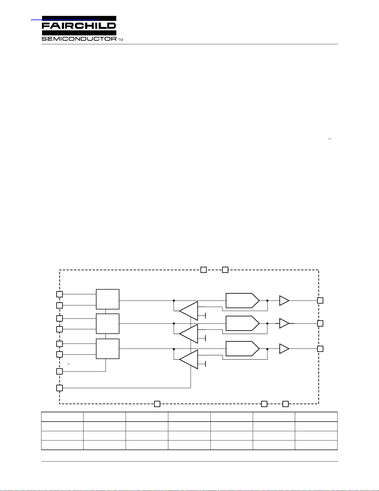
Block Diagram
RINA/YINA
2
RINB/YINB
5
GINA/UINA
6
GIN/UINB
7
BINA/VINA
8
BINB/VINB
9
A/B MUX
1
MUX
TRANSCONDUCTANCE
ERROR AMP
MUX
TRANSCONDUCTANCE
ERROR AMP
MUX
TRANSCONDUCTANCE
ERROR AMP
General Description
The ML6426 are a family of triple video filters with buffered
outputs. There are several versions of the ML6426, each with
different passband cut-off frequencies of 6.7MHz, 12MHz,
24MHz, 30MHz, and 36MHz. Each channel contains a 4
order Butterworth lowpass reconstruction video filter. The
filter is optimized for minimum overshoot and flat group
delay and guaranteed differential gain and phase at the outputs of the integrated cable drivers.
All input signals from DACs are AC coupled into the
ML6426. All channels have DC restore circuitry to clamp the
DC input levels during video H-sync, using an output feedback clamp. An external H-sync signal is required for this
purpose.
All outputs must be AC coupled into their loads. Each output
can drive 2V
2 (6dB) at 1V
12
V
CCO
+
–
0.5V
+
–
0.5V
+
–
0.5V
into a 150 Ω load. All channels have a gain of
P-P
input levels.
P-P
4
V
CC
R
4th-ORDER
FILTER A
4th-ORDER
FILTER B
4th-ORDER
FILTER C
×2
×2
×2
OUT/YOUT
G
OUT/UOUT
B
OUT/VOUT
th
-
13
11
10
SYNCIN
16
DISABLE
15
GNDO
14
GND
3
ML6426-1 ML6426-2 ML6426-3 ML6426-4 ML6426-5 ML6426-15
Filter A 6.7MHz 12MHz 24MHz 30MHz 36MHz 15MHz
Filter B 6.7MHz 12MHz 24MHz 30MHz 36MHz 15MHz
Filter C 6.7MHz 12MHz 24MHz 30MHz 36MHz 15MHz
REV. 3A August 2004
Page 2
A
B
A
B
A
B
ML6426 DATA SHEET
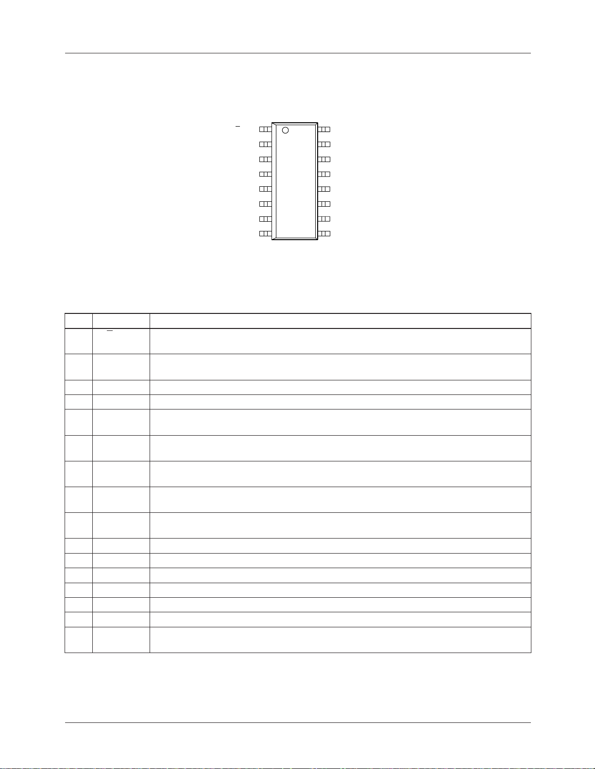
Pin Configuration
ML6426
16-Pin Narrow SOIC (S16N)
16
A/B MUX
RINA/YINA
GND
V
CC
RINB/YINB
GINA/UINA
GINB/UINB
BINA/VINA
1
2
3
4
5
6
7
8
TOP VIEW
SYNC IN
15
DISABLE
14
GNDO
13
R
OUT/YOUT
12
V
CCO
11
G
OUT/UOUT
10
B
OUT/VOUT
9
BINB/VINB
Pin Description
PIN NAME FUNCTION
1 A/B MUX Logic input pin to select between Bank <A> and Bank <B> video inputs . This pin is
internally pulled high.
2R
3 GND
4V
5R
6G
7G
8B
9B
10 B
11 G
12 V
13 R
14 GNDO
15 DISABLE Disable/Enable pin . Turns the chip off when logic high. Internally pulled low.
16 SYNC IN
A/Y
IN
CC
B/Y
IN
A/U
IN
B/U
IN
A/V
IN
B/V
IN
OUT
OUT
CCO
OUT
Unfiltered analog R- or Y-channel input for Bank <A> . Sync must be provided at
IN
SYNC IN pin.
Analog ground
Analog 5V supply
Unfiltered analog R- or Y-channel input for Bank <B> . Sync must be provided at
IN
SYNC IN pin.
Unfiltered analog G- or U-channel input for Bank <A> . Sync must be provided at
IN
SYNC IN pin.
Unfiltered analog G- or U-channel input for Bank <B> . Sync must be provided at
IN
SYNC IN pin.
Unfiltered analog B- or V-channel input for Bank <A> . Sync must be provided at
IN
SYNC IN pin.
Unfiltered analog B- or V-channel input for Bank <B> . Sync must be provided at
IN
SYNC IN pin.
Analog B or V-channel output
Analog G or U-channel output
5V power supply for output buffers
Analog R or Y-channel output
Analog ground
Input for an external H-sync logic signal for filter channels . CMOS level input.
Active High.
2
REV. 3A August 2004
Page 3
DATA SHEET ML6426
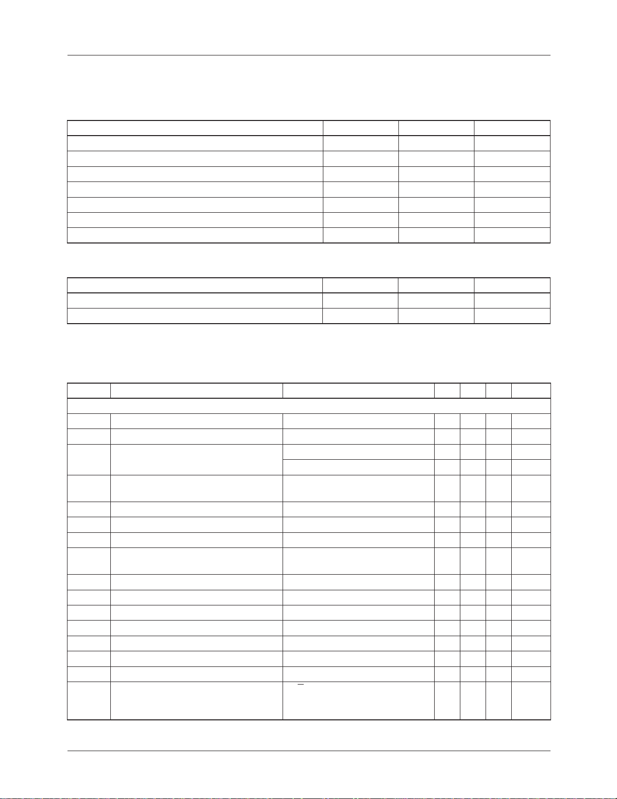
Absolute Maximum Ratings
Absolute maximum ratings are those values beyond which the device could be permanently damaged. Absolute maximum
ratings are stress ratings only and functional device operation is not implied.
Parameter Min. Max. Unit
V
CC
–0.3 7 V
Junction Temperature 150 °C
ESD >2000 V
Analog and Digital I/O GND – 0.3 V
+ 0.3 V
CC
Storage Temperature Range –65 150 °C
Lead Temperature (Soldering, 10 sec) 260 °C
Thermal Resistance ( θ
) 100 °C/W
JA
Operating Conditions
Parameter Min. Max. Unit
Temperature Range 0 70 °C
V
Range 4.5 5.5 V
CC
Electrical Characteristics
Unless otherwise specified, V
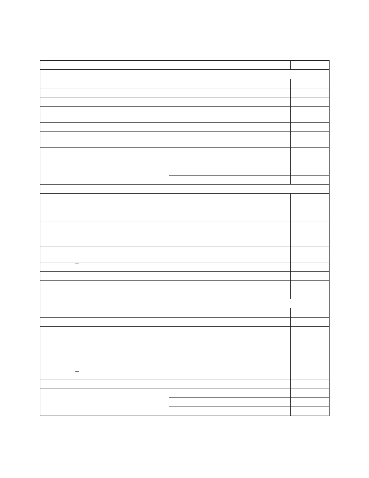
Symbol Parameter Conditions Min Typ Max Units
General
I
A
V
CC
V
OUT
Supply Current No Load (V
Low Frequency Gain (R, G, B) V
Output Level during Sync (R, G, B,)
Output Capability
t
CLAMP
V
I
Clamp Response Time Settled to Within 10mV,
Input Signal Dynamic Range (R, G, B,) AC Coupled 1.4 V
OS Peak Overshoot (R, G, B,) 2V
C
L
Output Load Capacitance (R, G, B,) All Outputs 35 pF
Output Load Drive Capability, per Pin
(YUV or RGB Outputs)
dG Differential Gain (R, G, B,) All Outputs at f
d φ
T
HD
Differential Phase (R, G, B,) All Outputs at f
Output Distortion (R, G, B,) V
PSRR PSRR (R, G, B,) 0.5V
I
SC
V
V
T
MUX
IH
IL
Output Short Circuit Current (R, G, B,) Note 2 120 mA
Input Voltage Logic High DISABLE, SYNC IN 2.5 V
Input Voltage Logic Low DISABLE, SYNC IN 1.0 V
Input Mux
Data Valid
Time
= 5V±10%, T
CC
= Operating Temperature Range (Note 1)
A
= 5.5V) 52 80 mA
CC
= 100mV
IN
at 100KHz 5.34 6.0 6.65 dB
P-P
DURING SYNC 0.7 0.9 1.2 V
RL = 150 Ω , AC-coupled@1MHz 2 V
10 ms
C
= 0.1µF
IN
Output Pulse 4.3 %
P-P
One Load is 150 Ω
C
C
OUT
= 2V
P-P
at 1 MHz 0.8 %
P-P
(100kHz) at V
A/B Mux
/2 0.4 %
/2 0.4 °
CC
2 loads
35 dB
2µs
Pin Valid
High or Low
P-P
P-P
REV. 3A August 2004
3
Page 4
≥
ML6426 DATA SHEET
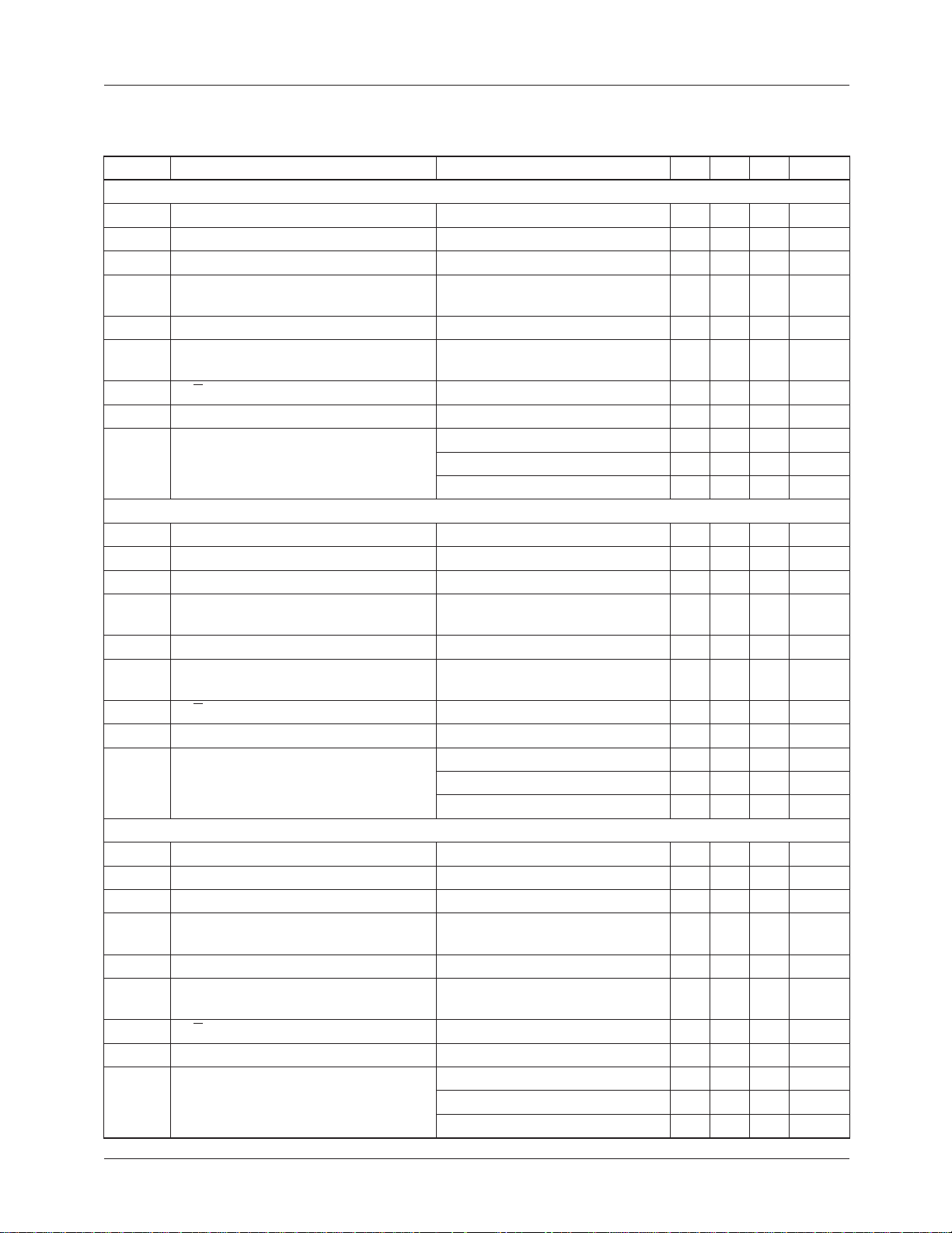
Electrical Characteristics (continued)
Unless otherwise specified, V
Symbol Parameter Conditions Min Typ Max Units
6.7MHz Filter: ML6426-1
f
1dB
f
c
f
0.8fc
f
SB
–1dB Bandwidth Flatness (R, G, B,) 25°C 4.0 4.8 MHz
–3dB Bandwidth Flatness (R, G, B,) 25°C 6.0 6.7 MHz
0.8 x f
Attenuation 1.5 dB
C
StopBand Rejection
(All Channels ≥ 4 f
NOISE Output Noise (R, G, B,) Fullband 1.0 mV
X
TALK
X
TALK
T
PD
T
PD
Crosstalk Input of 0.5V
A/B MUX Crosstalk Input of 0.5V
Group Delay (R, G, B,) 100kHz 70 ns
Group Delay Deviation from Flatness
(R, G, B,)
12MHz Filter: ML6426-2
f
1dB
f
c
f
0.8fc
f
SB
–1dB Bandwidth Flatness (R, G, B,) 25°C 7.8 9.2 MHz
–3dB Bandwidth Flatness (R, G, B,) 25°C 10.8 12 MHz
0.8 x f
Attenuation 1.2 dB
C
StopBand Rejection
(All Channels ≥ 4 f
NOISE Output Noise (R, G, B,) Fullband 1 mV
X
TALK
X
TALK
T
PD
∆T
PD
Crosstalk Input of 0.5V
A/B MUX Crosstalk Input of 0.5V
Group Delay (R, G, B,) 100kHz 40 ns
Group Delay Deviation from Flatness
(R, G, B,)
24MHz Filter: ML6426-3
f
1dB
f
c
f
0.8fc
f
SB
–1dB Bandwidth Flatness (R, G, B,) 25°C 13.6 16 MHz
–3dB Bandwidth Flatness (R, G, B,) 25°C 21.6 24 MHz
0.8 x fC Attenuation 1.7 dB
StopBand Rejection
(All Channels ≥ 4 fC)
NOISE Output Noise (R, G, B,) Fullband 1.0 mV
X
TALK
X
TALK
T
PD
∆T
PD
Crosstalk Input of 0.5V
A/B MUX Crosstalk Input of 0.5V
Group Delay (R, G, B,) 100kHz 22 ns
Group Delay Deviation from Flatness
(R, G, B,)
= 5V±10%, TA = Operating Temperature Range (Note 1)
CC
f
4 fC, Note 3 –38 –42 dB
IN
)
C
at 1 MHz
P-P
Between any two Channels
at 3.58/4.43MHz –54 dB
P-P
to 3.58MHz 4.0 ns
to 4.43MHz 8.0 ns
to 10MHz 9 ns
f
≥ 4 fC, Note 3 –40 dB
IN
)
C
at 1 MHz
P-P
Between any two Channels
at 3.58/4.43MHz –54 dB
P-P
to 3.58MHz 1 ns
to 4.43MHz 1 ns
to 10MHz 7 ns
fIN ≥ 4 fC, Note 3 –40 dB
at 1 MHz
P-P
Between any two Channels
at 3.58/4.43MHz -54 dB
P-P
to 3.58MHz 1 ns
to 4.43MHz 1 ns
to 10MHz 2 ns
RMS
–55 dB
RMS
–55 dB
RMS
–55 dB
∆
4
REV. 3A August 2004
Page 5
DATA SHEET ML6426
Electrical Characteristics (continued)
Unless otherwise specified, V
Symbol Parameter Conditions Min Typ Max Units
30MHz Filter: ML6426-4
f
1dB
f
c
f
0.8fc
f
SB
–1dB Bandwidth Flatness (R, G, B,) 25°C 15.3 18 MHz
–3dB Bandwidth Flatness (R, G, B,) 25°C 27 30 MHz
0.8 x fC Attenuation 1.7 dB
StopBand Rejection
(All Channels ≥ 4 f
NOISE Output Noise (R, G, B,) Fullband 1.0 mV
X
TALK
X
TALK
T
PD
∆T
PD
Crosstalk Input of 0.5V
A/B MUX Crosstalk Input of 0.5V
Group Delay (R, G, B,) 100kHz 18 ns
Group Delay Deviation from Flatness
(R, G, B,)
36MHz Filter: ML6426-5
f
1dB
f
c
f
0.8fc
f
SB
–1dB Bandwidth Flatness (R, G, B,) 25°C 17 20 MHz
–3dB Bandwidth Flatness (R, G, B,) 25°C 32.4 36 MHz
0.8 x fC Attenuation 2 dB
StopBand Rejection
(All Channels ≥ 4 fC)
NOISE Output Noise (R, G, B,) Fullband 1.0 mV
X
TALK
X
TALK
T
PD
∆T
PD
Crosstalk Input of 0.5V
A/B MUX Crosstalk Input of 0.5V
Group Delay (R, G, B,) 100kHz 17 ns
Group Delay Deviation from Flatness
(R, G, B,)
15MHz Filter: ML6426-15
f
1dB
f
c
f
0.8fc
f
SB
–1dB Bandwidth Flatness (R, G, B,) 25°C 10.8 12.2 MHz
–3dB Bandwidth Flatness (R, G, B,) 25°C 13.8 15 MHz
0.8 x fC Attenuation 1.2 dB
StopBand Rejection (All Channels ≥ 4 fC)
NOISE Output Noise (R, G, B,) Fullband 1.0 mV
X
TALK
X
TALK
T
PD
∆T
PD
Crosstalk Input of 0.5V
A/B MUX Crosstalk Input of 0.5V
Group Delay (R, G, B,) 100kHz 40 ns
Group Delay Deviation from Flatness
(R, G, B,)
Notes
1. Limits are guaranteed by 100% testing, sampling, or correlation with worst case test conditions.
2. Sustained short circuit protection limited to 10 seconds.
3. 38dB is based on tester noise limits.
= 5V±10%, TA = Operating Temperature Range (Note 1)
CC
≥ 4 fC, Note 3 -40 dB
f
IN
)
C
at 1 MHz
P-P
Between any two Channels
at 3.58/4.43MHz -54 dB
P-P
to 10MHz 0.5 ns
to 27MHz 2 ns
fIN ≥ 4 fC, Note 3 –40 dB
at 1 MHz
P-P
Between any two Channels
at 3.58/4.43MHz –54 dB
P-P
to 10MHz 0.5 ns
to 30MHz 4 ns
fIN ≥ 4 fC, Note 3 –40 dB
at 1 MHz
P-P
Between any two Channels
at 3.58/4.43MHz –54 dB
P-P
to 3.58MHz 1 ns
to 4.43MHz 1 ns
to 10MHz 9 ns
RMS
-55 dB
RMS
–55 dB
RMS
–55 dB
REV. 3A August 2004 5
Page 6
ML6426 DATA SHEET
Functional Description
The ML6426 is a triple monolithic continuous time video
filter designed for reconstructing video signals from an
YUV/RGB video D/A source. The ML6426 is intended for
use in AC coupled input and output applications.
The filters approximate a 4th-order Butterworth characteristic with an optimization toward low overshoot and flat group
delay. All outputs are capable of driving 2V
coupled 150Ω video loads, with up to 35pF of load capacitance. All outputs are capable of driving a 75Ω load at 1V
All channels are clamped during sync to establish the appropriate output voltage swing range (DC restore). Thus the
input coupling capacitors do not behave according to the
RINA/YINA
2
R
IN
G
IN
B
IN
SYNC IN
0.1µF
0.1µF
0.1µF
RINB/YINB
5
GINA/UINA
6
GINB/UINB
7
BINA/VINA
8
BINB/VINB
9
A/B MUX
1
SYNCIN
16
MUX
TRANSCONDUCTANCE
MUX
TRANSCONDUCTANCE
MUX
TRANSCONDUCTANCE
ACTIVE HIGH
into AC
P-P
ERROR AMP
ERROR AMP
ERROR AMP
DISABLE
15
P-P
conventional RC time constant. In most applications, the
ML6426's input coupling capacitors are only 0.1µF.
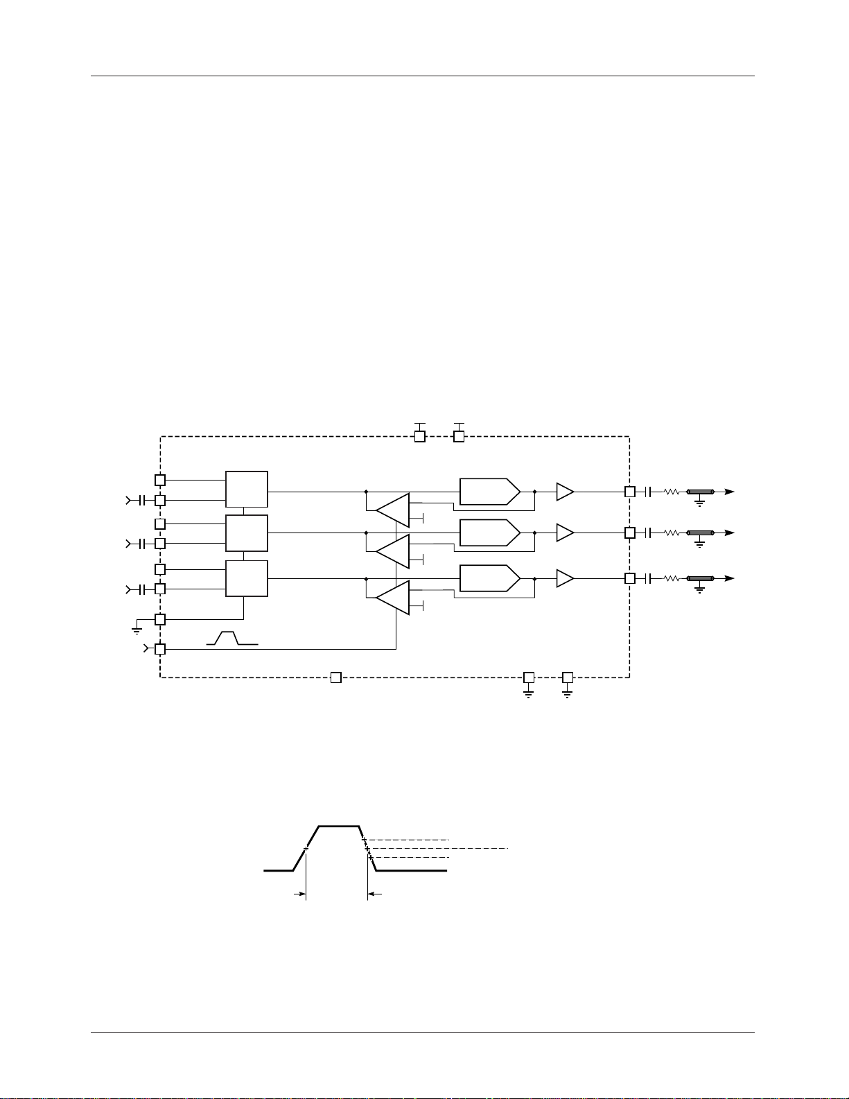
An external CMOS compatible HSYNC pulse is required
which is Active High on the SYNC IN Pin. See Figure 2.
During sync, the feedback clamp sources/sinks current to
restore the DC level. The net result is that the average input
current is zero. Any change in the input coupling capacitors'
value will linearly affect the clamp response times.
Each channel is essentially tilt-free. Each input is clamped
.
by a feedback amp which responds to the output during sync.
The ML6426 is robust and stable under all stated load and
input conditions. Bypassing both V
pins directly to
CC
ground ensures this performance.
5V 5V
12
0.5V
0.5V
0.5V
4
V
CC
4th-ORDER
FILTER A
4th-ORDER
FILTER B
4th-ORDER
FILTER C
GNDO
14
×2
×2
×2
GND
R
G
B
3
OUT/YOUT
OUT/UOUT
OUT/VOUT
220µF
75Ω
13
220µF
75Ω
11
220µF
75Ω
10
V
CCO
+
–
+
–
+
–
R
G
B
Figure 1. Typical Application Schematic
V
= 2.5V
PW
MIN
IH
VIL = 1.0V
= 2µS
50% x V
SYNC IN
Figure 2. SYNC IN Pulse Width
6 REV. 3A August 2004
Page 7
DATA SHEET ML6426
Typical Applications
onto the CRT at 30Hz. Excessive large area flicker would
result. Such kinds of flicker can be seen on a PAL display
Reconstruction filter selection for HDTV and
VGA signal filtering
The filtering requirements for HDTV and VGA standards
vary depending on the resolution of the image to be displayed, and its refresh rate. The actual refresh rate of the display is not necessarily the same as the transmission rate of
the frames of images. Some formats use a frame rate of
with its brightness set high. To avoid this, the video will need
to be stored in a frame buffer. This buffer already exists in
the MPEG decoder of HDTV systems, so there is no cost
penalty. The buffer is read out at twice the rate as the frame
rate for 30Hz systems, thus getting us a refresh rate of 60Hz.
Similar things are done for the 24Hz frame rate formats to
boost them to a 60Hz refresh rate.
30Hz, but the display of those formats cannot be scanned
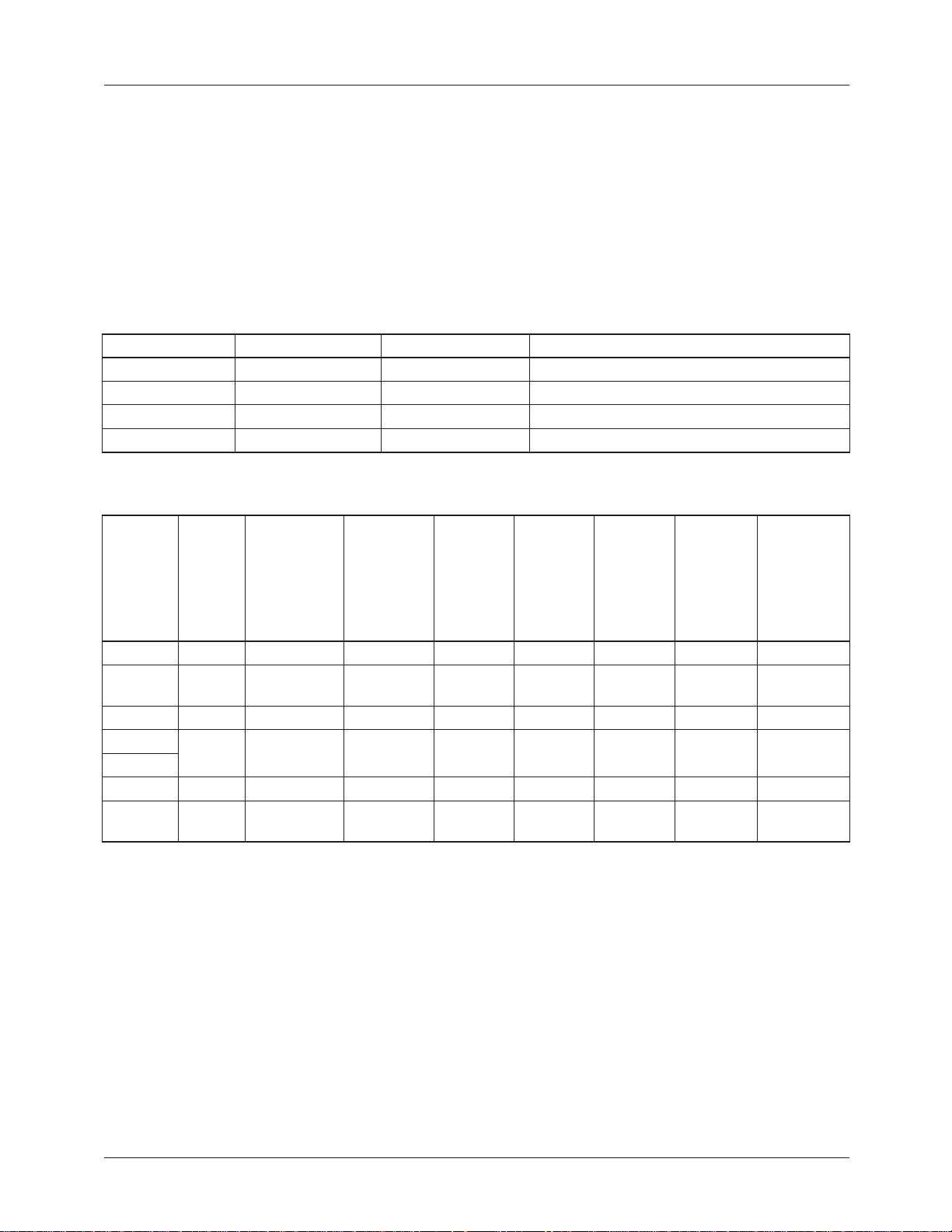
Table 1. HDTV / Advanced TV Applications: (From Table 10.3 from ATSC document A54)
Pixels Vertical Lines Aspect Ratio Picture Transmission Rate
1920 1080 16:9 60I, 30P, 24P
1280 720 16:9 60P, 30P, 24P
704 480 16:9 and 4:3 60P, 60I, 30P, 24P
640 480 4:3 60P, 60I, 30P, 24P
P=progressive scan, I=interlaced scan
Table 2. Choosing the Correct Reconstruction Filter and Video Amplifier for TV Applications, ML6426 options
Standard
Pixels
Vertical
Lines
Picture
Transmission
Rate (Note 2)
Display
Refresh
Rate (Note 2)
1920 1080 30P, 24P 60Hz 70.6KHz 162MHz 81MHz N/A
SMPTE 1280 720 60P, 30P,
60Hz 47.1KHz 60MHz 30MHz ML6426-5
24P
704 480 (Note 1) 60I 60Hz 15.7KHz 13.5MHz 6.75MHz ML6426-1
704 480 60P, 30P,
60Hz 31KHz 27MHz 13.5MHz ML6426-2
24P
640 480 (Note 1) 60I 60Hz 15.7KHz 24.5MHz 12MHz ML6426-2
640 480 60P, 30P,
60Hz 31KHz 12.27MHz 6MHz ML6426-1
24P
P=progressive scan, I=interlaced scan, na = not available
Notes
1. NTSC display rates, can be fed directly into NTSC encoder (set top box)
2. 60 Hz also includes 59.94Hz
3. Custom frequencies ranging ± 3 to 6MHz can be special cut to order
Approximate
Horizontal
Rate
Approximate
Sample Clock
Approximate
Reconstruction
Filter Cutoff
ML6426-4
ML6426-4
Fairchild
Filter to Use
(Note 3)
REV. 3A August 2004 7
Page 8
ML6426 DATA SHEET
Pixel clock rates for the output D/A converters can be
roughly determined from the Table 1. Don’t forget that the
deflection system of a CRT display needs retrace time for the
vertical and horizontal.
This retrace time can vary from one design of an HDTV set
to another, as it only involves tradeoffs between the frame
buffer in the MPEG decoder and the CRT deflection system.
Allowing for 10% retrace time for the vertical and 20% for
the horizontal, the appropriate Reconstruction Filter is summarized in Table 2.
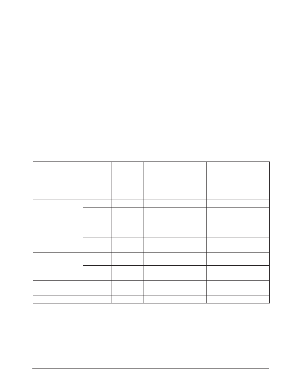
For VGA or RGB monitors, the following resolutions can
use the corresponding Reconstruction Filter and Video
Amplifier as shown in Table 3.
Using the ML6426 in Multiple Resolutions
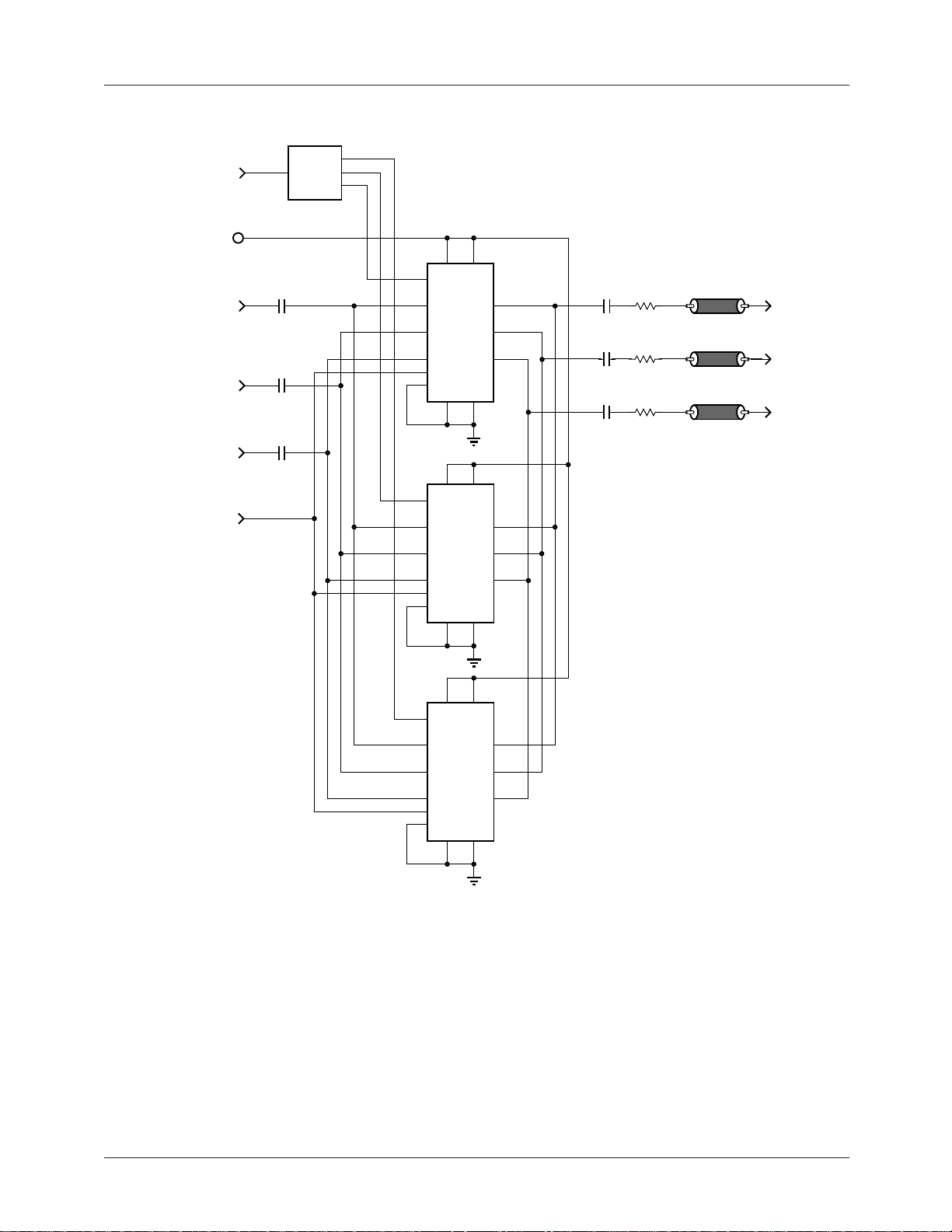
Several ML6426 devices can be used in parallel to construct
a selectable filter selection block ranging from frequencies
between 6.7 MHz to 50MHz. Each ML6426 can be individually controlled via the disable pin. In a parallel configuration,
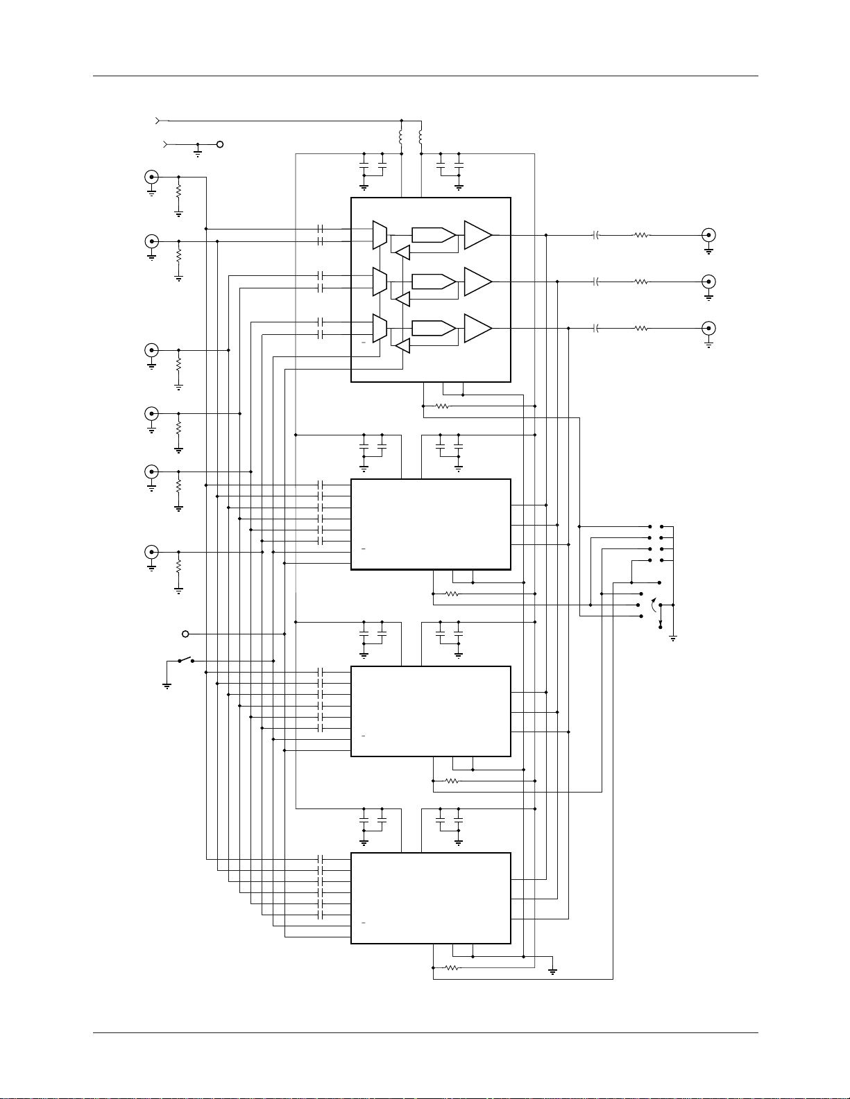
as shown in Figure 3 and 7, several ML6426 devices can be
used and selected via general purpose I/O or other logic to
perform the proper reconstruction filtering for the resolution
of choice. This configuration allows for a minimum of bill of
materials and reduces cost. Fairchild’s ML6426 EVAL Kit
demonstrates multi-resolution designs. Furthermore, since
the ML6426 pin-out is identical for all the options, the filters
can be interchanged. This allows for ease of product migration to integrate newer resolutions to filter and drive various
DAC outputs at different sampling frequencies.
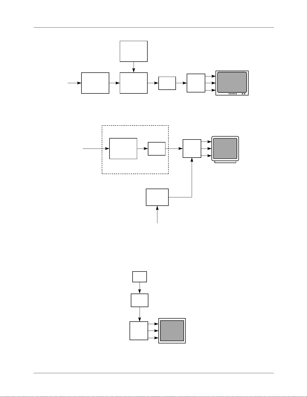
Figures 4, 5, and 6 show system diagrams when the ML6426
provides a good solution. Figure 7 provides a more detailed
description for advanced TV applications using various resolutions for legacy video, SDTV, and HDTV.
Table 3. Choosing the Correct Reconstruction Filter and Video Amplifier for TV Applications, ML6426 options
Pixels
Vertical
Lines
Name
Refresh Rate
(Prog except noted)
Horizontal Rate
Sample Clock
Reconstruction
Filter Cutoff
640 480 VGA 60Hz 31.5kHz 25.175MHz 12.5MHz ML6426-2
VGA 72Hz 37.9kHz 31.5MHz 15.5MHz ML6426-3
VGA 75Hz 37.5kHz 31.5MHz 15.5MHz ML6426-3
800 600 SVGA 56Hz 35.1kHz 36MHz 18MHz ML6426-3
SVGA 60Hz 37.9kHz 40MHz 20MHz ML6426-3
SVGA 72Hz 48.1kHz 50MHz 25MHz ML6426-3
SVGA 75Hz 46.9kHz 49.5MHz 25MHz ML6426-3
1024 768 XGA 43Hz
35.5kHz 44.9MHz 23MHz ML6426-3
Interlaced
XGA 60Hz 37.9kHz 65MHz 33MHz ML6426-5
XGA 70Hz 56.5kHz 75MHz 37.5MHz ML6426-5
1280 1024 SXGA 75Hz 80kHz 135MHz 68MHz na
SXGA 60Hz 113MHz 57MHz na
1600 1200 UXGA 60Hz 166MHz 83MHz na
N/A = not available
Fairchild
Filter to Use
8 REV. 3A August 2004
Page 9
DATA SHEET ML6426
GENERAL
PURPOSE I/O
5V
YIN/R
UIN/G
VIN/B
SYNC IN
SELECT
LOGIC
0.1µF
IN
0.1µF
IN
0.1µF
IN
DISABLE/ENABLE LINES
12 4
15
2
5
6
7
8
9
16
1
15
2
5
6
7
8
9
16
1
ML6426-1
6.7MHz
14 3
12 4
ML6426-2
12MHz
13
11
10
13
11
10
220µF
220µF
220µF
75Ω
75Ω
75Ω
R/Y
G/U
B/V
14 3
12 4
15
2
5
6
7
8
9
16
1
ML6426-5
36MHz
14 3
13
11
10
Figure 3. ATSC Digital Television Application
REV. 3A August 2004 9
Page 10
ML6426 DATA SHEET
GRAPHIC
PROCESSOR
FROM SAT
OR CABLE
FROM
CAMERA
VCR
MPEG2
TRANSPORT
AND DECODER
Figure 4. Digital TV Receiver or HDTV Decoder Box
CV
S-VIDEO
ANALOG
HDTV
DECODER
AND DISPLAY
PROCESSOR
VIDEO
DECODER
AND DISPLAY
PROCESSOR
D/A
VIDEO
ENCODER
YCrCb
DIGITAL
FROM
DVD-ROM
OR MEMORY
D/A
RGB
ML6426
ML6426
Y
U
V
Y
U
V
DIGITAL TV
RGB
MONITOR
Figure 5. PC Graphics/Frame Grabber Editing Card
MRI, XRAY,
ULTRASOUND, CT SCAN
DSP
DIGITAL YUV
D/A
ANALOG
Y
ML6426
U
V
MEDICAL
IMAGING
Figure 6. PC MRI, XRAY, Ultrasound, CT Scan
10 REV. 3A August 2004
Page 11
DATA SHEET ML6426
5V
GND
RINA/YINA
RINB/YINB
GINA/UINA
GINB/UINB
BINA/VINA
BINB/VINB
HYSYNC IN
SW2
R5
75Ω
R7
75Ω
R8
75Ω
R9
75Ω
R10
75Ω
R6
75Ω
GND
C 17
C 18
C 19
C 20
C 21
C 22
C 23
C 24
C 25
C 26
C 27
C 28
C 29
C 30
C 31
C 32
C 33
C 34
0.1µF
0.1µF
0.1µF
0.1µF
0.1µF
0.1µF
0.1µF
0.1µF
0.1µF
0.1µF
0.1µF
0.1µF
0.1µF
0.1µF
0.1µF
0.1µF
0.1µF
0.1µF
16
0.1µF
16
0.1µF
16
C10
0.1µF
2
5
6
7
8
9
1
C12
2
5
6
7
8
9
1
C14
2
5
6
7
8
9
1
RINA
RINB
GINA
GINB
BINA
BINB
A/B
MUX
SYNC IN
RINA
RINB
GNA
GNB
BINA
BINB
A/B MUX
SYNC IN
RINA
RINB
GNA
GNB
BINA
BINB
A/B MUX
SYNC IN
C2
1µF
C4
1µF
C6
1µF
FB1
12
4
CCO
V
4TH ORDER
FILTER
4TH ORDER
FILTER
4TH ORDER
FILTER
12
4
CCO
V
ML6426-3
12
4
CCO
V
ML6426-4
FB2
C1
1µF
CC
V
DISABLE
15
C3
1µF
CC
V
U2
15
C5
1µF
CC
V
U3
15
GNDO
14
R1 47kΩ
DISABLE
14
DISABLE
14
C9
0.1µF
ML6426-1
GND
3
C11
0.1µF
GNDO
GND
3
R2 47kΩ
C13
0.1µF
GNDO
GND
3
R3 47kΩ
U1
R
OUT
13
G
OUT
11
B
OUT
10
13
R
OUT
11
G
OUT
10
B
OUT
13
R
OUT
11
G
OUT
10
B
OUT
C 41 220µF
C 42 220µF
C 43 220µF
R11
75Ω
R12
75Ω
R13
75Ω
R
OUT/YOUT
G
OUT/UOUT
B
OUT/VOUT
JP1
2
1
4
3
6
5
8
7
4
3
SWI
2
1
0
C8
C 35
C 36
C 37
C 38
C 39
C 40
0.1µF
0.1µF
0.1µF
0.1µF
0.1µF
0.1µF
0.1µF
16
C16
2
5
6
7
8
9
1
RINA
RINB
GNA
GNB
BINA
BINB
A/B MUX
SYNC IN
1µF
12
CCO
V
ML6426-X
4
V
1µF
CC
UX
C7
DISABLE
15
GNDO
14
C15
0.1µF
GND
3
R4 47kΩ
13
R
OUT
11
G
OUT
10
B
OUT
Figure 7. Typical Applications Schematic
REV. 3A August 2004 11
Page 12
ML6426 DATA SHEET
Performance Data
10
0
–10
–20
–30
–40
AMPLITUDE (dB)
–50
–60
–70
0.01 1 100
0.1 10
FREQUENCY (MHz)
10
0
–10
–20
–30
–40
AMPLITUDE (dB)
–50
–60
–70
10k 100k 1M 10M
FREQUENCY (Hz)
100M 1G
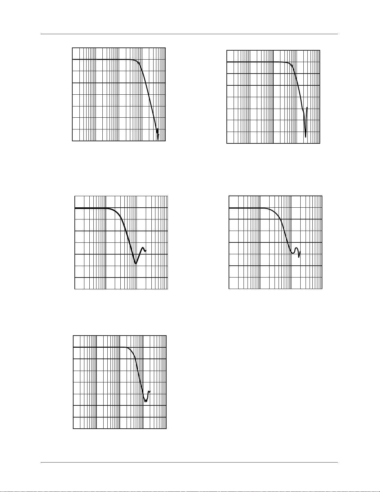
Figure 8. Passband Flatness all Outputs
(Normalized) 6.7 MHz, ML6426CS-1
10
0
–10
–20
–30
–40
AMPLITUDE (dB)
–50
–60
–70
1M 10M 100M
FREQUENCY (MHz)
Figure 10. Passband Flatness all Outputs
(Normalized) 24 MHz, ML6426CS-3
10
Figure 9. Passband Flatness all Outputs
(Normalized) 12 MHz, ML6426CS-2
10
0
–10
–20
–30
–40
AMPLITUDE (dB)
–50
–60
–70
1M 10M 100M
FREQUENCY (MHz)
Figure 11. Passband Flatness all Outputs
(Normalized) 30 MHz, ML6426CS-4
0
–10
–20
–30
–40
AMPLITUDE (dB)
–50
–60
–70
100k 1M 10M
FREQUENCY (Hz)
100M 1G
Figure 12. Passband Flatness all Outputs
(Normalized) 36MHz, ML6426CS-5
12 REV. 3A August 2004
Page 13
DATA SHEET ML6426
0
–10
–20
–30
–40
–50
–60
AMPLITUDE (dB)
–70
–80
–90
–100
10 50
20 60
04080
30 70 90
FREQUENCY (MHz)
100
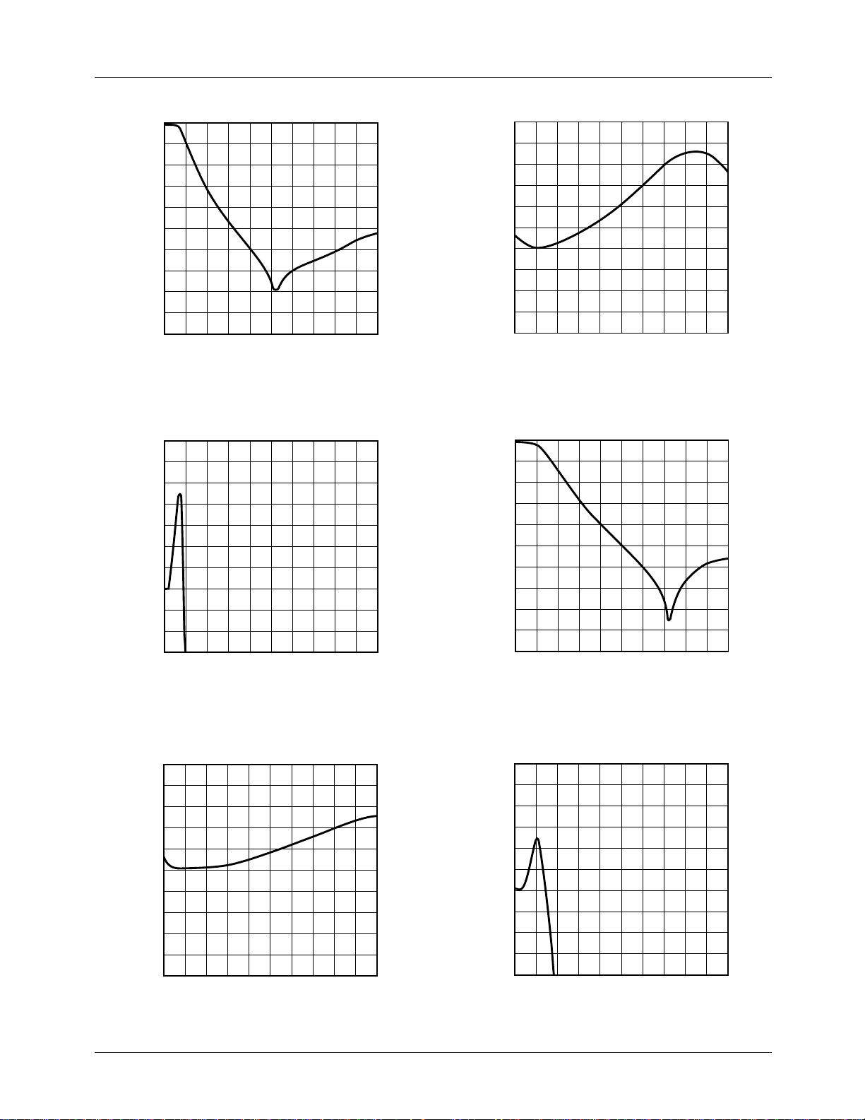
Figure 13. Frequency Response All Outputs
ML6426-CS-1
14
12
10
8
6
4
2
0
–2
GROUP DELAY DEVIATION (ns)
–4
–6
10 50
20 60
04080
30 70 90
FREQUENCY (MHz)
100
Figure 15. Group Delay Deviation All band,
All Outputs ML6426CS-1
12
10
8
6
4
2
0
–2
–4
GROUP DELAY DEVIATION (ns)
–6
–8
0.7 3.5
1.4 4.2
0 2.8 5.6
2.1 4.9 6.3
FREQUENCY (MHz)
7.0
Figure 14. Group Delay Deviation of Passband,
All Outputs ML6426CS-1
0
–10
–20
–30
–40
–50
–60
AMPLITUDE (dB)
–70
–80
–90
–100
20 60
10 50
04080
30 70 90
FREQUENCY (MHz)
100
Figure 16. Frequency Response All Outputs
ML6426CS-2
10
8
6
4
2
0
–2
–4
–6
GROUP DELAY DEVIATION (ns)
–8
–10
15
26
048
379
FREQUENCY (MHz)
10
Figure 17. Group Delay Deviation of Passband,
All Outputs ML6426CS-2
12
10
8
6
4
2
0
–2
–4
GROUP DELAY DEVIATION (ns)
–6
–8
10 50
20 60
04080
30 70 90
FREQUENCY (MHz)
Figure 18. Group Delay Deviation All Band,
All Outputs ML6426CS-2
100
REV. 3A August 2004 13
Page 14
ML6426 DATA SHEET
0
–10
–20
–30
–40
–50
–60
AMPLITUDE (dB)
–70
–80
–90
–100
10 50
20 60
04080
30 70 90
FREQUENCY (MHz)
100
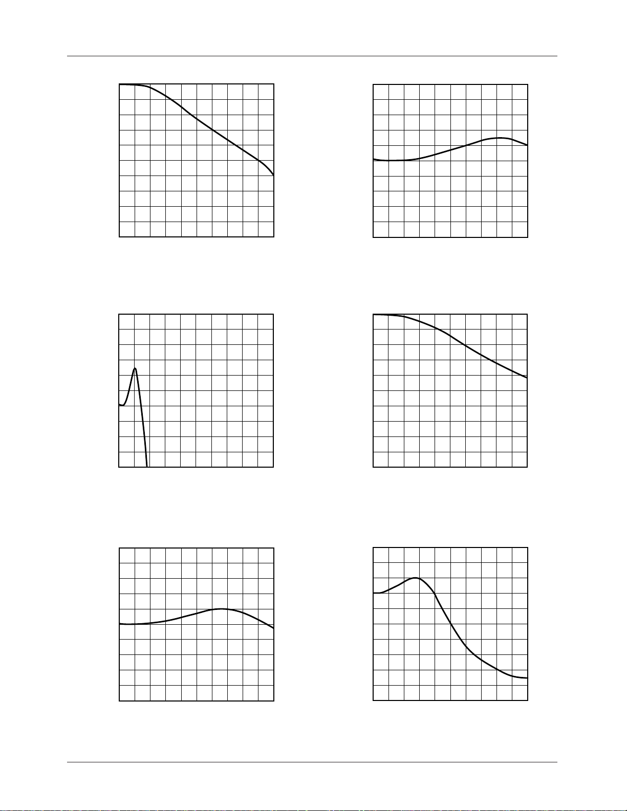
Figure 19. Frequency Response All Outputs
ML6426CS-3
12
10
8
6
4
2
0
–2
–4
GROUP DELAY DEVIATION (ns)
–6
–8
10 50
20 60
04080
30 70 90
FREQUENCY (MHz)
100
Figure 21. Group Delay Deviation All Band,
All Outputs ML6426CS-3
10
8
6
4
2
0
–2
–4
–6
GROUP DELAY DEVIATION (ns)
–8
–10
2.5 12.5
515
01020
7.5 17.5 22.5
FREQUENCY (MHz)
25
Figure 20. Group Delay Deviation of Passband,
All Outputs ML6426CS-3
0
–10
–20
–30
–40
–50
–60
AMPLITUDE (dB)
–70
–80
–90
–100
10 50
20 60
04080
30 70 90
FREQUENCY (MHz)
100
Figure 22. Frequency Response All Outputs
ML6426CS-4
10
8
6
4
2
0
–2
–4
–6
GROUP DELAY DEVIATION (ns)
–8
–10
420
824
01632
12 28 36
FREQUENCY (MHz)
40
Figure 23. Group Delay Deviation of Passband,
All Outputs ML6426CS-4
6
4
2
0
–2
–4
–6
–8
–10
GROUP DELAY DEVIATION (ns)
–12
–14
10 50
20 60
04080
30 70 90
FREQUENCY (MHz)
Figure 24. Group Delay Deviation All Band,
All Outputs ML6426CS-4
100
14 REV. 3A August 2004
Page 15
DATA SHEET ML6426
0
–10
–20
–30
–40
–50
–60
AMPLITUDE (dB)
–70
–80
–90
–100
10 50
20 60
04080
30 70 90
FREQUENCY (MHz)
100
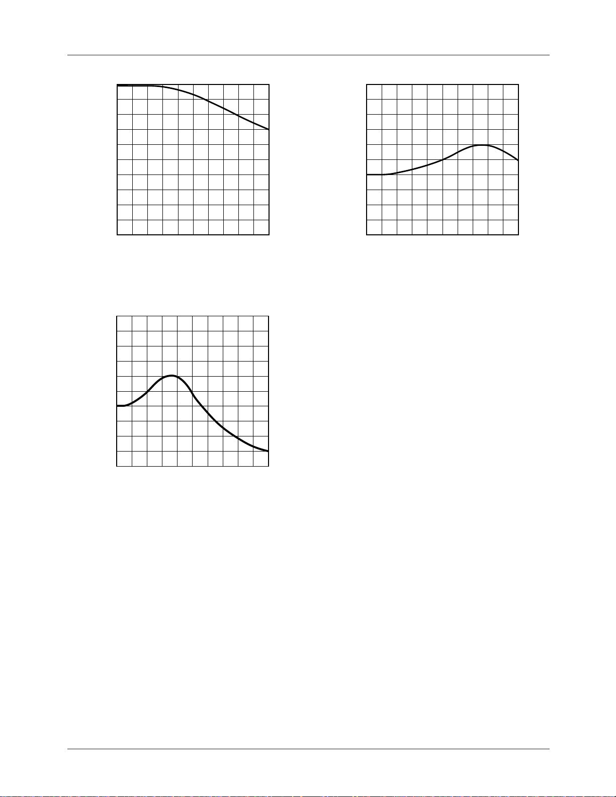
Figure 25. Frequency Response All Outputs
ML6426-CS-5
12
10
8
6
4
2
0
–2
–4
GROUP DELAY DEVIATION (ns)
–6
–8
10 50
20 60
04080
30 70 90
FREQUENCY (MHz)
100
Figure 27. Group Delay Deviation All band,
All Outputs ML6426CS-5
12
10
8
6
4
2
0
–2
–4
GROUP DELAY DEVIATION (ns)
–6
–8
525
10 30
02040
15 35 45
FREQUENCY (MHz)
50
Figure 26. Group Delay Deviation of Passband,
All Outputs ML6426CS-5
REV. 3A August 2004 15
Page 16
ML6426 DATA SHEET
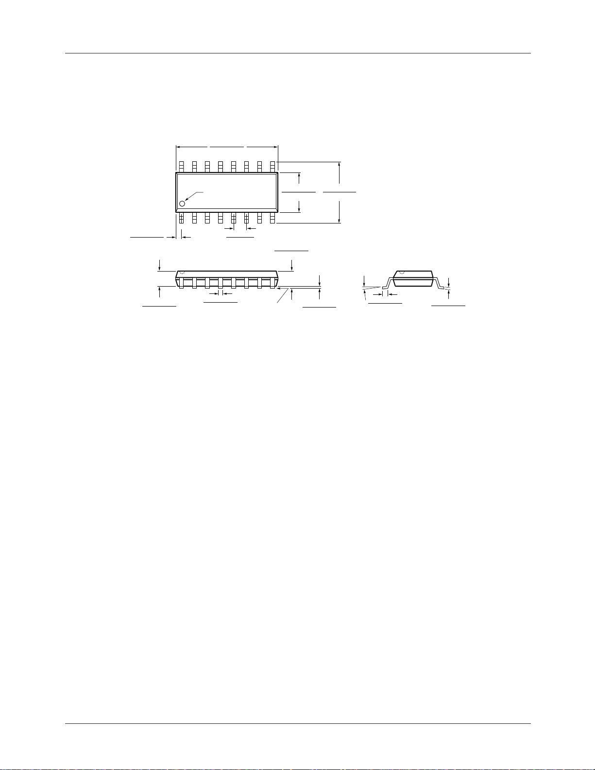
Mechanical Dimensions
Package: S16N
16-Pin Narrow SOIC
0.386 - 0.396
16
(9.80 - 10.06)
0.017 - 0.027
(0.43 - 0.69)
( 4 PLA CES)
0.055 - 0.061
(1.40 - 1.55)
1
PI N 1 I D
0.050 BSC
(1.27 BSC)
0.012 - 0.020
(0.30 - 0.51)
0.148 - 0.158
(3.76 - 4.01)
0.059 - 0.069
(1.49 - 1.75)
SEATI NG PLANE
0.228 - 0.244
(5.79 - 6.20)
0.004 - 0.010
(0.10 - 0.26)
0° - 8°
0.015 - 0.035
(0.38 - 0.89)
0.006 - 0.010
(0.15 - 0.26)
16 REV. 3A August 2004
Page 17
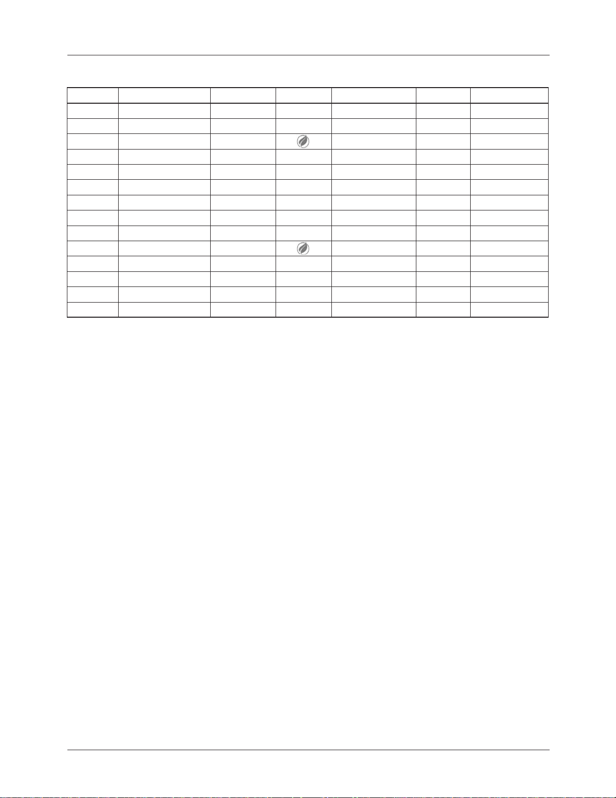
ML6426 DATA SHEET
Ordering Information
Model Part Number Cuttoff Freq Lead Free Package Container Pack Quantity
ML6426 ML6426CS1 6.7MHz SOIC-16 (Narrow) Rail 48
ML6426 ML6426CS1X 6.7MHz SOIC-16 (Narrow) Reel 2500
ML6426 ML6426CS1X_NL 6.7MHz SOIC-16 (Narrow) Reel 2500
ML6426 ML6426CS2 12MHz SOIC-16 (Narrow) Rail 48
ML6426 ML6426CS2X 12MHz SOIC-16 (Narrow) Reel 2500
ML6426 ML6426CS3 24MHz SOIC-16 (Narrow) Rail 48
ML6426 ML6426CS3X 24MHz SOIC-16 (Narrow) Reel 2500
ML6426 ML6426CS4 30MHz SOIC-16 (Narrow) Raill 48
ML6426 ML6426CS4X 30MHz SOIC-16 (Narrow) Reel 2500
ML6426 ML6426CS4X_NL 30MHz SOIC-16 (Narrow) Reel 2500
ML6426 ML6426CS5 36MHz SOIC-16 (Narrow) Rail 48
ML6426 ML6426CS5X 36MHz SOIC-16 (Narrow) Reel 2500
ML6426 ML6426CS15 15MHz SOIC-16 (Narrow) Rail 48
ML6426 ML6426CS15X 15MHz SOIC-16 (Narrow) Reel 2500
Temperature range for all parts: 0°C to +70°C
DISCLAIMER
FAIRCHILD SEMICONDUCTOR RESERVES THE RIGHT TO MAKE CHANGES WITHOUT FURTHER NOTICE TO
ANY PRODUCTS HEREIN TO IMPROVE RELIABILITY, FUNCTION OR DESIGN. FAIRCHILD DOES NOT ASSUME
ANY LIABILITY ARISING OUT OF THE APPLICATION OR USE OF ANY PRODUCT OR CIRCUIT DESCRIBED HEREIN;
NEITHER DOES IT CONVEY ANY LICENSE UNDER ITS PATENT RIGHTS, NOR THE RIGHTS OF OTHERS.
LIFE SUPPORT POLICY
FAIRCHILD’S PRODUCTS ARE NOT AUTHORIZED FOR USE AS CRITICAL COMPONENTS IN LIFE SUPPORT DEVICES
OR SYSTEMS WITHOUT THE EXPRESS WRITTEN APPROVAL OF THE PRESIDENT OF FAIRCHILD SEMICONDUCTOR
CORPORATION. As used herein:
1. Life support devices or systems are devices or systems
which, (a) are intended for surgical implant into the body,
or (b) support or sustain life, and (c) whose failure to
perform when properly used in accordance with
instructions for use provided in the labeling, can be
reasonably expected to result in a significant injury of the
user.
www.fairchildsemi.com
2. A critical component in any component of a life support
device or system whose failure to perform can be
reasonably expected to cause the failure of the life support
device or system, or to affect its safety or effectiveness.
© 2004 Fairchild Semiconductor Corporation
 Loading...