

Page 1
www.fairchildsemi.com
ML6416
S-Video Filter with Summed Composite Output,
Sound Trap, and Group Delay Compensation
Features
• 7.1MHz Y and C filters, with CV out
• 14dB notch at 4.5MHz for sound trap
• 42dB stopband attenuation at 27MHz on Y, C, and CV
• Better than 1dB flatness to 4.5 MHz on Y, C, and CV
• RF Modulator output differential group delay between
400kHz and 3.58MHz is typically -170ns.
• No external frequency select components or clocks
• 9ns group delay flatness on Y, C, and CV output
• AC coupled inputs and outputs
• 0.4% differential gain on Y, C and CV channels, 0.4º
differential phase on Y, C and CV channels
• 0.8% total harmonic distortion on all channels
• DC restore with low tilt
Applications
• Cable Set-top Boxes
• Satellite Set-top Boxes
• DVD Players
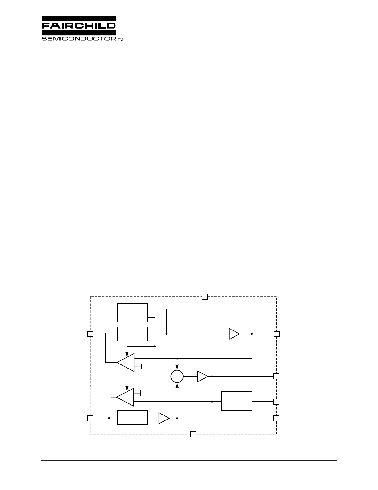
Block Diagram
General Description
The ML6416 is a dual Y/C 4th-order Butterworth lowpass
video filter optimized for minimum overshoot and flat group
delay. The device also contains a summing circuit to generate filtered composite video, an audio trap and group delay
compensation circuit to notch-out audio, providing an area
for the addition of the FM audio carrier(s) and mimic the
group delay distortion introduced at the transmitter. The
group delay predistortion compensates for the nominal TV
receiver IF filter distortion.
In a typical application, the Y and C input signals from
DACs are AC coupled into the filter. Both channels have DC
restore circuitry to clamp the DC input levels during video
sync. The Y and C channels use a separate feedback clamp.
The clamp pulse is derived from the Y channel.
The outputs are AC coupled. The Y, C, CV, and modulator
outputs can drive 2V
into a 150Ω load (1V
P-P
load). The Y, C, CV, and notch channels have a gain of
approximately 2 (6dB) with 1V
input levels.
P-P
75Ω coax
P-P
YIN
CIN
VCC
7
SYNC STRIP,
REFERENCE,
AND TIMING
1
4
4TH – ORDER
FILTER
gM
1V
gM
4TH – ORDER
FILTER
1V
+
Σ
+
×2
×2
3
GND
×2
NOTCH,
GROUP
DELAY
YOUT
8
CVOUT
6
RF MOD
2
COUT
5
REV. 1.0.6 8/26/02
Page 2
ML6416 PRODUCT SPECIFICATION
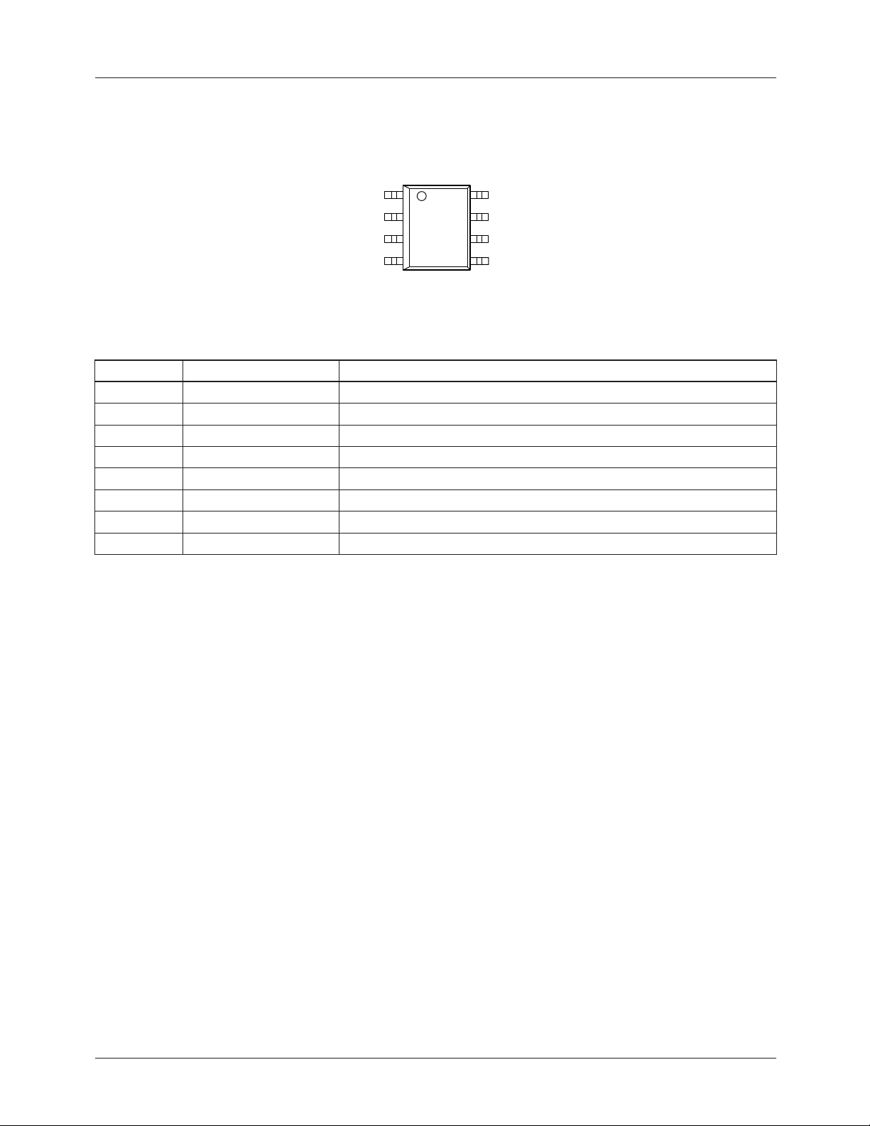
Pin Configuration
ML6416
8-Pin SOIC (S08)
YIN
RF MOD
GND
CIN
1
2
3
4
TOP VIEW
8
YOUT
7
VCC
6
CVOUT
5
COUT
Pin Descriptions
Pin # Signal Name Description
1 YIN Luminance input
2 RF MOD Output to RF modulator driver
3 GND Ground
4 CIN Chrominance input
5 COUT Chrominance output
6 CVOUT Composite video output
7 VCC 5V supply
8 YOUT Luminance output
Functional Description
Introduction
This product is a dual monolithic continuous time video filter
designed for reconstructing the luminance and chrominance
signals from an S-Video D/A source. Composite video output is generated by summing the Y and C outputs. The chip
is intended for use in applications with AC coupled input and
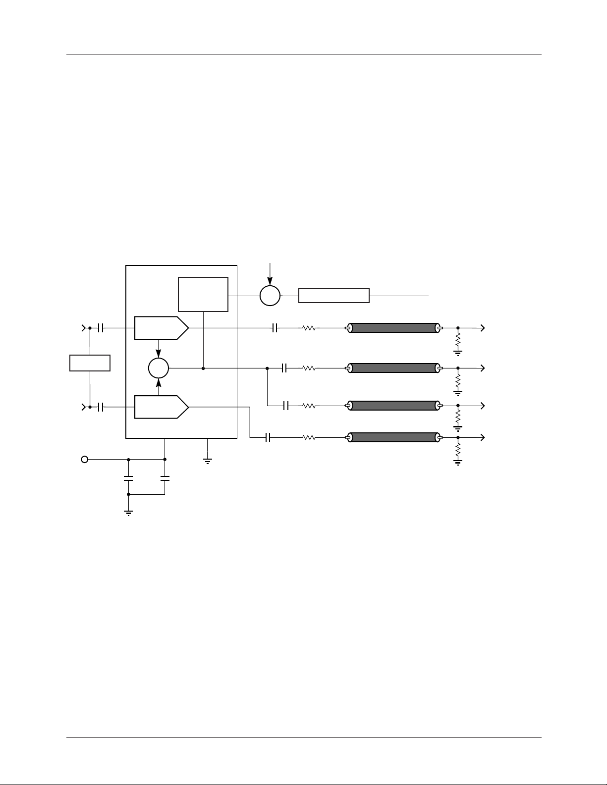
AC coupled outputs. (See Figure 1)
The reconstruction filters approximate a 4th-order Butterworth characteristic with an optimization toward low overshoot and flat group delay. Y, C, and CV outputs are capable
of driving 2V
to 35pF of load capacitance at the output pin.
All channels are clamped during sync to establish the appropriate output voltage swing range. Thus the input coupling
capacitors do not behave according to the conventional RC
time constant. Clamping for all channels settles to less than
10mv within 5ms of a change in video input sources.
In most applications the input coupling capacitors are 0.1µF.
The Y and C input typically sinks 1µA during active video,
into AC coupled 150Ω video loads, with up
P-P
which nominally tilts a horizontal line by about 2mV at the Y
output. During sync, the clamp typically sources 20µA to
restore the DC level. The net result is that the average input
current is zero.
Any change in the input coupling capacitor’s value will
inversely alter the amount of tilt per line. Such a change will
also linearly affect the clamp response times.
This product is robust and stable under all stated load and
input conditions. Capacitive bypassing VCC directly to
ground ensures this performance.
Luminance (Y) I/O
The luma input is driven by either a low impedance source of
1V
or the output of a 75Ω terminated line. The input is
P-P
required to be AC coupled via a 0.1µF coupling capacitor
which allows for a settling time of 5ms. The luma output is
capable of driving an AC coupled 150Ω load at 2V
1V
into a 75Ω load. Up to 35pF of load capacitance
P-P
(at the output pin) can be driven without stability or slew
issues. The output is AC coupled with a 220µF or larger AC
coupling capacitor.
P-P
, or
2 REV. 1.0.6 8/26/02
Page 3
PRODUCT SPECIFICATION ML6416
Chrominance (C) I/O
The chroma input is driven by a low impedance source of
0.7V
or the output of a 75Ω terminated line. The input is
P-P
required to be AC coupled via a 0.1µF coupling capacitor
which allows for a clamp setting time of 5ms. The chroma
output is capable of driving an AC coupled 150Ω load at
2V
P-P
, or 1V
into a 75Ω load. Up to 35pF of load capaci-
P-P
tance can be driven without stability or slew issues. A 0.1µF
AC coupling capacitor is recommended at the output.
(This reduces the circuit cost as chroma does not contain
low frequency components.)
Typical Applications Diagram
4.5MHz FM SOUND
+
NOTCH
YIN
ENCODER
CIN
5.0V
0.1µF
0.1µF
1
4
4th-ORDER
FILTER
+
Σ
+
4th-ORDER
FILTER
AND GROUP
DELAY
PROTECTION
2
Σ
220µF
8
6
5
37
220µF
220
0.1µF
Composite Video (CV) Output
The composite video output is capable of driving 2 loads to
2V
. It is intended to drive a TV and a VCR. Either the TV
P-P
input or the VCR input can be shorted to ground and the
other output will still meet specifications. Up to 35pF of load
capacitance (at the output pin) can be driven without stability
or slew issues.
RF Modulator Output
The RF modulator output is capable of driving a 600Ω load
to 2V
VIDEO MODULATOR
75Ω
75Ω
µF
75Ω
75Ω
, but is primarily intended to drive a modulator load.
P-P
TO CHANNEL 3 OR 4
VIDEO CABLES
75Ω
75Ω
75Ω
75Ω
YOUT
TO TV
CVOUT TO VCR
COUT
1µF0.1µF
Figure 1. Coupled S-Video, Composite Video Line Driver, Sound Trap, and Group Delay Pre-distortion
REV. 1.0.6 8/26/02 3
Page 4

ML6416 PRODUCT SPECIFICATION
Absolute Maximum Ratings
Absolute maximum ratings are those values beyond which the device could be permanently damaged. Absolute maximum
ratings are stress ratings only and functional device operation is not implied.
Parameter Min. Max. Units
DC Supply Voltage –0.3 7 V
Analog & Digital I/O GND – 0.3 V
+ 0.3 V
CC
Output Current (Continuous)
CV Channel
C and Y Channels
60
30
mA
mA
Junction Temperature 150 °C
Storage Temperature Range –65 150 °C
Lead Temperature (Soldering, 10s) 260 °C
Thermal Resistance (θ
) 115 °C/W
JA
Operating Conditions
Parameter Min. Max. Units
Temperature Range 0 70 °C
VCC Range 4.5 5.5 V
Electrical Characteristics
Unless otherwise specified, VCC = 5.0V ±10%, All inputs AC coupled with 100nF, TA = Operating Temperature Range
Symbol Parameter Conditions Min. Typ. Max. Units
I
CC
V
CC
AV
YC
AV
RFMOD
AV
CV
tCLAMP Clamp Response Time (Y Channel) Settled to Within 10mV, 0.1µF cap
f
1dB
f
C
f
SB
V
i
I
SC
Supply Current 60 85 mA
Supply Range 4.5 5.0 5.5 V
Low Frequency Gain (Y
OUT
, C
) at 400KHz 5.75 6.0 6.25 dB
OUT
Low Frequency Gain (RFMOD) at 400KHz 6.1 6.7 7.3 dB
Low Frequency Gain (CV
C
Output Level (During Sync) Sync Present on Y
OUT
Y
Output Level (During Sync) Sync Present on Y
OUT
CV
Output Level (During Sync) Sync Present on Y
OUT
RFMOD Output Level (During Sync) Sync Present on Y
) at 400KHz 5.55 5.9 6.25 dB
OUT
IN
IN
IN
IN
1.6 2.0 2.4 V
0.75 1.0 1.25 V
0.75 1.0 1.25 V
0.65 1.0 1.35 V
59ms
–1.0dB Bandwidth (Flatness)
(Y
OUT
, C
OUT
, and CV
OUT
)
–3dB Bandwidth (Flatness)
(Y
, C
OUT
Stopband Rejection (Y
and CV
OUT
OUT
, and CV
)
OUT
OUT
)
, C
Input Signal Dynamic Range
OUT
on YIN and C
No Peaking Cap (Note 1) 4.2 4.5 MHz
,
fIN = 27MHz -37 –42 dB
AC Coupled 1.2 1.4 V
IN
6.7 7.1 MHz
(All Channels)
Output Short Circuit Current
(All Channels)
C
, Y
OUT
OUT
GND (Note 2)
, CV
, RFMOD to
OUT
40 80 mA
P-P
4 REV. 1.0.6 8/26/02
Page 5

PRODUCT SPECIFICATION ML6416
Electrical Characteristics (continued)
Unless otherwise specified, VCC = 5.0V ±10%, All inputs AC coupled with 100nF, TA = Operating Temperature Range
Symbol Parameter Conditions Min. Typ. Max. Units
CL Output Shunt Capacitance (All
Channels) (Note 5)
dG Differential Gain (Note 5) Y
dP Differential Phase (Note 5) Y
THD Output Distortion (All Channels)
(Note 5)
XTALK Crosstalk (Note 5) From C
PSRR PSRR (All Channels) (Note 5) 0.5V
SNR Y, C Channel (Note 5) NTC-7 weighting 4.2 MHz lowpass -65 -75 dB
CV Channel (Note 5) NTC-7 weighting 4.2 MHz lowpass -60 -70 dB
RFMOD Channel (Note 5) NTC-7 weighting 4.2 MHz lowpass -55 -65 dB
tpd Propagation Delay (Y, C, CV)
(Note 5)
∆tpd Group Delay Deviation from Flatness
(Y, C, and CV) (Note 5)
tSKEW Skew Between Y
OUT
and C
OUT
(Note 5)
T
CLDCV
T
CLGCV
GD
MOD
T
CLDMOD
T
CLGMOD
dG
RFMOD
dP
RFMOD
Chroma-Luma Delay C
Chroma-Luma Gain C
VOUT
VOUT
Group Delay RFMOD f = 3.58MHz (referenced to 400kHz) -205 -170 -135 ns
Chroma-Luminance Delay RFMOD f = 3.58MHz (referenced to 400kHz) -185 -150 -115 ns
Chroma-Luminance Gain RFMOD f = 3.58MHz (referenced to 400kHz) 95 100 105 %
Differential Gain RFMOD Channel 1.5 4 %
Differential Phase RFMOD Channel 1.0 1.5 °
pK Gain Peaking (Note 3) RFMOD Channel at 2.0MHz 0.5 0.75 dB
MCF Modulator Channel Flatness (Note 3) at 3.75MHz -0.5 -0.1 +0.75 dB
AV Notch Attenuation (Note 3) From 4.425MHz to 4.63MHz 14 dB
AV Notch Attenuation (Note 3) At 4.2MHz 5 dB
T
PASS
Passband Group Delay, RFMOD
(Note 4)
Notes
1. Peaking capacitor increases CV output at 4.2MHz nominally by 0.7dB
2. Sustained short circuit protection limited to 10 seconds
3. Referenced to 400kHz
4. Group Delay is tested down to 400kHz but guaranteed by design to 200kHz.
5. Guaranteed by characterization
All Outputs 35 pF
, C
OUT
, C
OUT
VOUT = 1.8V
OUT
OUT
, and CV
, and CV
, Y/C Out at
P-P
OUT
OUT
0.4 1 %
0.4 1 °
0.8 1.0 %
3.58MHz
of 0.5V
IN
3.58MHz to Y
From YIN Input of 0.4V
3.58MHz, to C
(100KHz) at VCC -30 -40 dB
P-P
OUT
OUT
P-P
at
P-P
at
-45 -55 dB
-50 -58 dB
30 70 110 ns
to 3.58MHz (NTSC) 9 ns
at 1MHz 0 ns
f = 3.58 MHz (referenced to 400kHz) -35 0 35 ns
f = 3.58 MHz (referenced to 400kHz) 92 95 104 %
f = 200kHz to f = 3MHz -50 50 ns
REV. 1.0.6 8/26/02 5
Page 6

ML6416 PRODUCT SPECIFICATION
Mechanical Dimensions Inches (millimeters)
Package: S08
8-Pin SOIC
0.189 - 0.199
(4.80 - 5.06)
8
0.017 - 0.027
(0.43 - 0.69)
(4 PLACES)
0.055 - 0.061
(1.40 - 1.55)
PIN 1 ID
1
0.050 BSC
(1.27 BSC)
0.012 - 0.020
(0.30 - 0.51)
SEATING PLANE
0.148 - 0.158
(3.76 - 4.01)
0.059 - 0.069
(1.49 - 1.75)
0.228 - 0.244
(5.79 - 6.20)
0.004 - 0.010
(0.10 - 0.26)
0° - 8°
0.015 - 0.035
(0.38 - 0.89)
0.006 - 0.010
(0.15 - 0.26)
6 REV. 1.0.6 8/26/02
Page 7

ML6416 PRODUCT SPECIFICATION
Ordering Information
Part Number Temperature Range Package
ML6416CS 0° to 70° 8 Pin SOIC (S08)
DISCLAIMER
FAIRCHILD SEMICONDUCTOR RESERVES THE RIGHT TO MAKE CHANGES WITHOUT FURTHER NOTICE TO
ANY PRODUCTS HEREIN TO IMPROVE RELIABILITY, FUNCTION OR DESIGN. FAIRCHILD DOES NOT ASSUME
ANY LIABILITY ARISING OUT OF THE APPLICATION OR USE OF ANY PRODUCT OR CIRCUIT DESCRIBED HEREIN;
NEITHER DOES IT CONVEY ANY LICENSE UNDER ITS PATENT RIGHTS, NOR THE RIGHTS OF OTHERS.
LIFE SUPPORT POLICY
FAIRCHILD’S PRODUCTS ARE NOT AUTHORIZED FOR USE AS CRITICAL COMPONENTS IN LIFE SUPPORT DEVICES
OR SYSTEMS WITHOUT THE EXPRESS WRITTEN APPROVAL OF THE PRESIDENT OF FAIRCHILD SEMICONDUCTOR
CORPORATION. As used herein:
1. Life support devices or systems are devices or systems
which, (a) are intended for surgical implant into the body,
or (b) support or sustain life, and (c) whose failure to
perform when properly used in accordance with
2. A critical component in any component of a life support
device or system whose failure to perform can be
reasonably expected to cause the failure of the life support
device or system, or to affect its safety or effectiveness.
instructions for use provided in the labeling, can be
reasonably expected to result in a significant injury of the
user.
www.fairchildsemi.com
8/26/02 0.0m 001
2001 Fairchild Semiconductor Corporation
Stock#DS30006416
 Loading...