

Page 1

E2E0057-29-71
¡ Semiconductor ML63512A/63514A
¡ Semiconductor
This version: Jul. 1999
Previous version: Jun. 1999
ML63512A/63514A
4-Bit Microcontroller with Built-in Level Detector, Melody Circuit, and Comparator,
Operating at 0.9 V (Min.)
GENERAL DESCRIPTION
The ML63512A/63514A is a CMOS 4-bit microcontroller with built-in level detector and
operates at 0.9 V (min.).
The ML63512A/63514A is an M6351x series mask ROM-version product of OLMS-63K family,
which employs Oki's original CPU core nX-4/250.
The program memory capacity and data memory capacity of the ML63512A differ from those of
the ML63514A.
48-pin TQFP and 64-pin TQFP packages are available for the ML63512A and ML63514A.
FEATURES
• Extensive instruction set
407 instructions
Transfer, rotate, increment/decrement, arithmetic operations, comparison, logic operations,
mask operations, bit operations, ROM table reference, stack operations, flag operations,
jump, conditional branch, call/return, control.
• Wide variety selection of addressing modes
Indirect addressing of four data memory types, with current bank register, extra bank
register, HL register and XY register.
Data memory bank internal direct addressing mode.
• Processing speed
Two clocks per machine cycle, with most instructions executed in one machine cycle.
Minimum instruction execution time : 61 ms (@ 32.768 kHz system clock)
1 ms (@ 2 MHz system clock)
• Clock generation circuit
Low-speed clock : Crystal oscillation or RC oscillation selectable by
mask option (30 to 80 kHz)
High-speed clock : Ceramic oscillation or RC oscillation selectable by
mask option (2 MHz max.)
• Program memory space
ML63512A: 4K words
ML63514A: 8K words
Basic instruction length is 16 bits/1 word
• Data memory space
ML63512A: 128 nibbles
ML63514A: 256 nibbles
1/29
Page 2

¡ Semiconductor ML63512A/63514A
• Stack level
Call stack level : 16 levels
Register stack level : 16 levels
• I/O ports
Input ports: Selectable as input with pull-up resistor/high-impedance input
Output ports: N-channel open drain output (can directly drive LEDs)
Input-output ports: Selectable as input with pull-up resistor/high-impedance input
Selectable as N-channel open drain output/CMOS output
Can be interfaced with external peripherals that use a different power supply than this device
uses. (Power to the output port is supplied from V
(separate power suply))
DDI
Number of ports:
(For 48-pin packages)
Input port : 1 port ¥ 4 bits
Output port : 1 port ¥ 4 bits
Input-output port : 6 ports ¥ 4 bits
(For 64-pin packages)
Input port : 1 port ¥ 4 bits
Output port : 1 port ¥ 4 bits
Input-output port : 9 ports ¥ 4 bits
• Melody output function
Melody sound frequency : 529 to 2979 Hz (@ 32.768 kHz)
Tone length : 63 varieties
Tempo : 15 varieties
Melody data : Stored in the program memory
Number of ports : 1 (dedicated pin)
Buzzer driver signal output : 4 kHz (@ 32.768 kHz)
• Level detector
Conversion time : Approx. 183 ms (@ 32.768 kHz)
Dedicated input pins : 2 pins (switched by software; for the secondary
functions of the input ports)
Detection level : 12 levels
• Comparator
Offset voltage : 50 mV max. (VDD = 1.5 V)
Comparison time : Approx. 183 ms (@ 32.768 kHz)
Number of channels : 1 (for the secondary functions of the input ports)
• Reset function
Reset through RESETB pin (RESETB pin can be pulled up by mask option)
• Power supply backup
Backup circuit (voltage multiplier) enables operation at 0.9 V minimum
2/29
Page 3

¡ Semiconductor ML63512A/63514A
• Timers and counter
8-bit timer ¥ 2
Selectable as auto-reload mode/capture mode/clock frequency measurement mode
15-bit time base counter ¥ 1
1 Hz, 2 Hz, 4 Hz, 8 Hz, 16 Hz, 32 Hz, 64 Hz, 128 Hz, 256 Hz, 512 Hz, 1 kHz, and 2 kHz signals
can be read (@ 32.768 kHz)
• Serial port
Mode : Selectable as UART mode/synchronous
mode
UART communication speed : 2TBCCLK, TBCCLK, 1/2TBCCLK, Timers 0
& 1 overflow
24 kbps Max. (when 2TBCCLK @ 80 kHz
selected)
Clock frequency in synchronous mode : 30 to 80 kHz (internal clock mode), external
clock frequency
Data length : 5 to 8 bits
• Interrupt sources
External interrupt (4 sources) : Selectable as rising edge/falling edge/both
rising and falling edges
Internal interrupt (10 sources) : Time base interrupt ¥ 4 (2, 4, 16, and 32 Hz
@ 32.768 kHz)
Timer interrupt ¥ 2
Level detector interrupt ¥ 1
Serial port reception interrupt ¥ 1
Serial port transmission interrupt ¥ 1
Melody end interrupt ¥ 1
• Operating Temperature
–20 to +70°C
• Supply voltage
When backup used : 0.9 to 1.8 V
(Maximum operating frequency 1 MHz)
When backup not used : 1.8 to 3.5 V
(When Level detector or Comparator is
used, maximum operating frequency
2 MHz)
1.8 to 5.5 V
(When Level detector and Comparator are
not used, maximum operating frequency
2 MHz)
• Package options:
48-pin plastic TQFP (TQFP48-P-0707-0.50-K) : (Product name: ML63512A-xxxTB,
ML63514A-xxxTB)
64-pin plastic TQFP (TQFP64-P-1010-0.50-K) : (Product name: ML63512A-xxxTP,
ML63514A-xxxTP)
xxx indicates a code number.
3/29
Page 4
¡ Semiconductor ML63512A/63514A
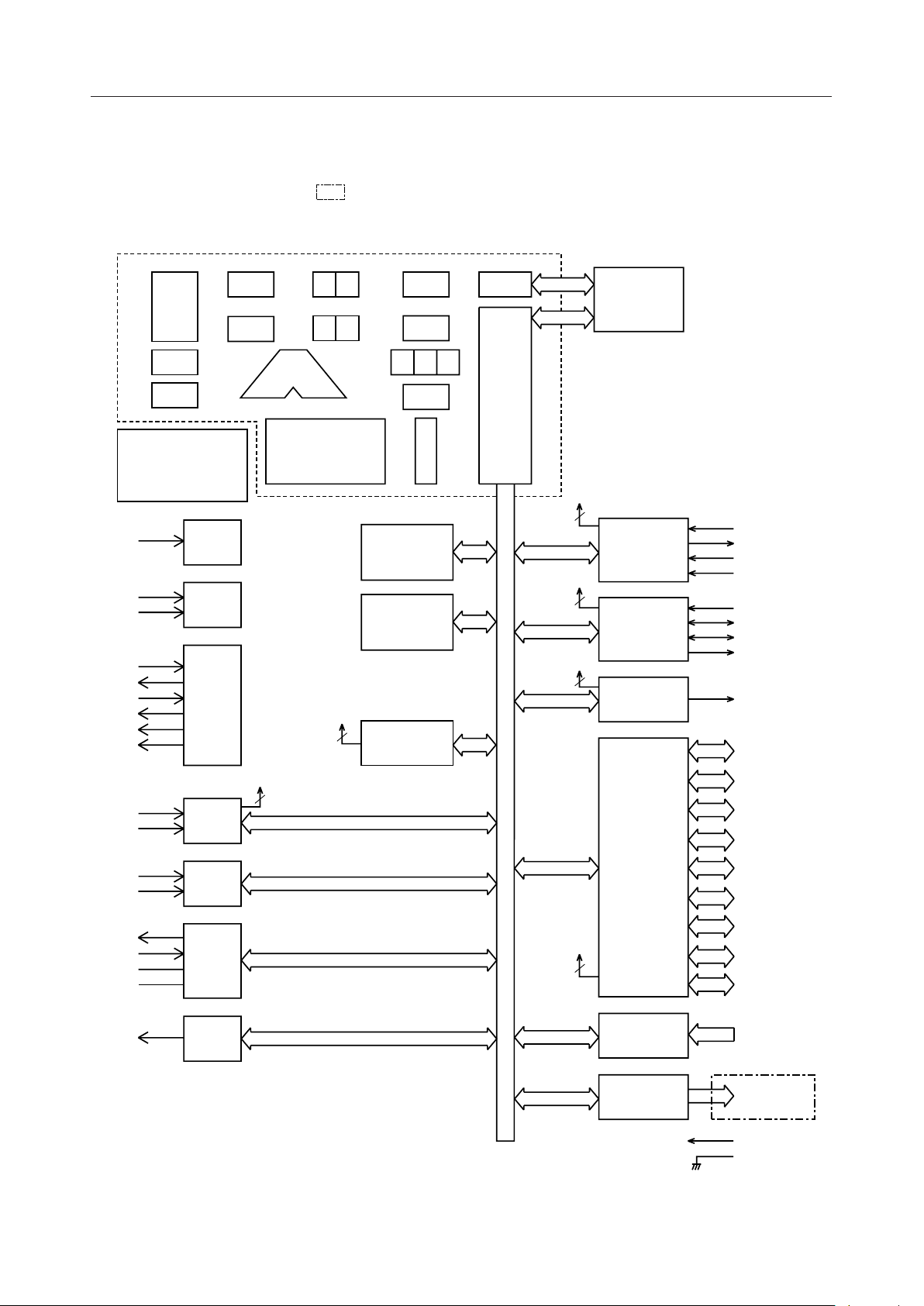
BLOCK DIAGRAM
An asterisk (*) indicates the port secondary function. The power to the circuits corresponding
to the signal names inside is supplied from V
nX-4/250
L
TIMING
CONTROL
CBR
EBR
H
YX
RA
A
(power supply for interface).
DDI
PC
ROM
ML63512A: 4KW
ML63514A: 8KW
RESETB
TST1B
TST2B
XT0
XT1
OSC0
OSC1
TBCCLK*
HSCLK*
LDIN0*
LDIN1*
CMPIN*
CMPREF*
V
DDH
V
DD
CB1
CB2
SP
RSP
STACK
CAL: 16-level
REG: 16-level
Detector
RST
TST
OSC
Level
CMP
BACK-
UP
INT
1
ALU
INSTRUCTION
DECODER
INT
4
C G
MIE
IR
RAM
ML63512A: 128N
ML63514A: 256N
INT
TBC
Z
BUS
CONTROL
INT
2
TIMER
8bit ¥ 2
INT
2
SIO
INT
1
MELODY
DATA BUS
I/O
PORT
INT
4
TM0CAP/TM1CAP*
TM0OVF/TM1OVF*
T0CK*
T1CK*
RXC*
TXC*
RXD*
TXD*
MD
P0.0-P0.3
P1.0-P1.3
P2.0-P2.3
P3.0-P3.3
P4.0-P4.3
P5.0-P5.3
=
P6.0-P6.3
=
P9.0-P9.3
PA.0-PA.3
=
V
DDL
=
Port 6 (P6.0 to P6.3), Port 9 (P9.0 to P9.3) and Port A (PA.0 to PA.3) are only provided for the 64-
VR
INPUT
PORT
OUTPUT
PORT
P7.0-P7.3
P8.0-P8.3
V
DDI
V
SS
pin packages.
4/29
Page 5
¡ Semiconductor ML63512A/63514A
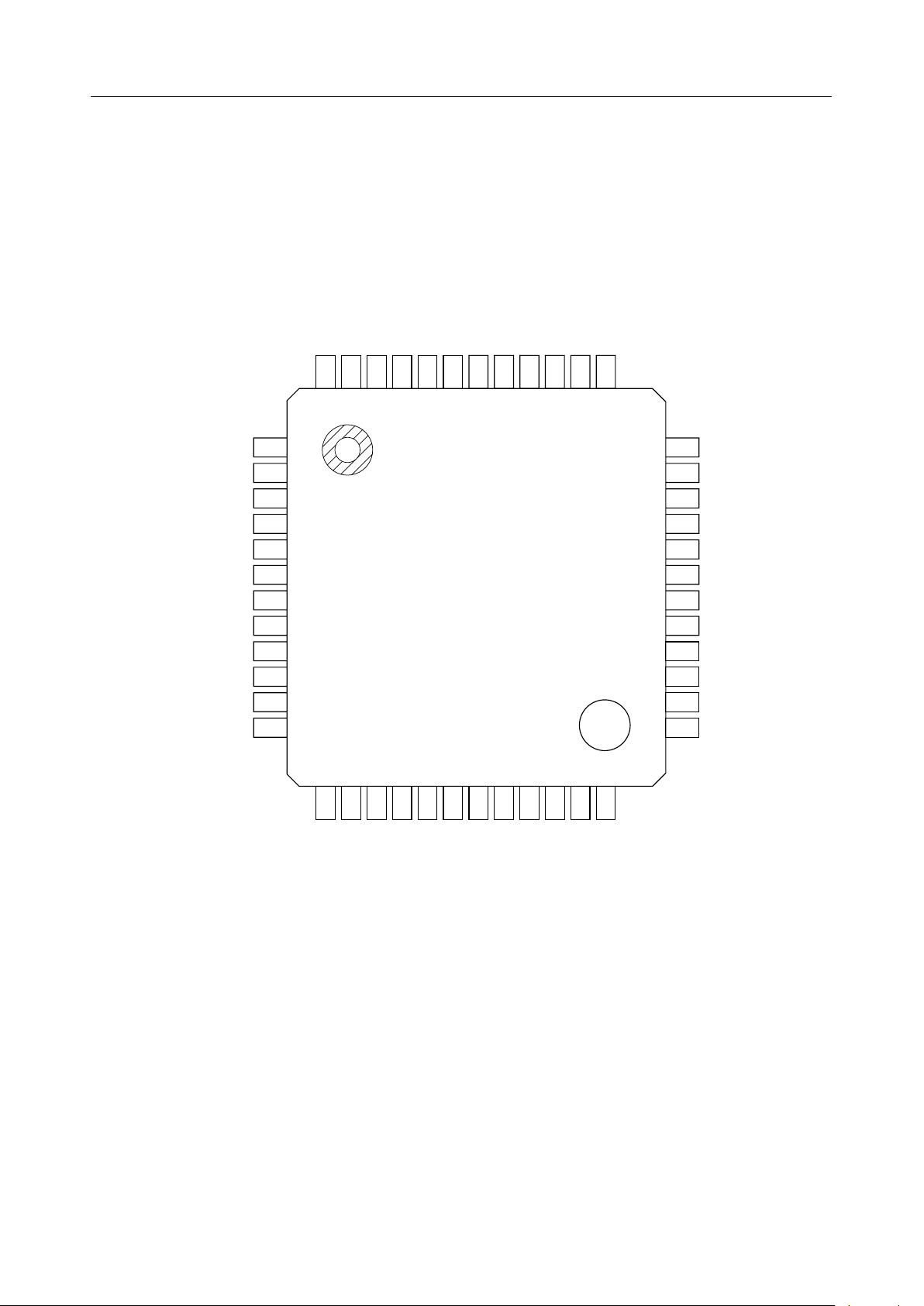
PIN CONFIGURATION (TOP VIEW)
P0.0/INT0
P0.1/INT1
P0.2/INT2
P0.3/INT3
P1.0/TM0CAP/TM0OVF
P1.1/TM1CAP/TM1OVF
P1.2/T0CK
P1.3/T1CK
P2.0/TBCCLK
P2.1/HSCLK
P2.2
P2.3
37
38
39
40
41
42
43
44
45
46
47
48
P3.0/RXD
P3.1/TXC
P3.2/RXC
P3.3/TXD
P4.0
P4.1
P4.2
P4.3
P5.0
P5.1
P5.2
P5.3
10
11
12
1
2
3
4
5
6
7
8
9
24
23
22
21
20
19
18
17
16
15
14
13
SS
DD
V
DDH
V
V
P7.0/CMPIN
P7.2/LDIN0
P7.1/CMPREF
P8.1
P8.0
P7.3/LDIN1
P8.2
P8.3
DDI
V
36
35
34
33
32
31
30
29
28
27
26
25
MD
RESETB
OSC1
OSC0
V
SS
TST2B
TST1B
XT1
XT0
V
DDL
CB2
CB1
48-Pin Plastic TQFP
5/29
Page 6
¡ Semiconductor ML63512A/63514A
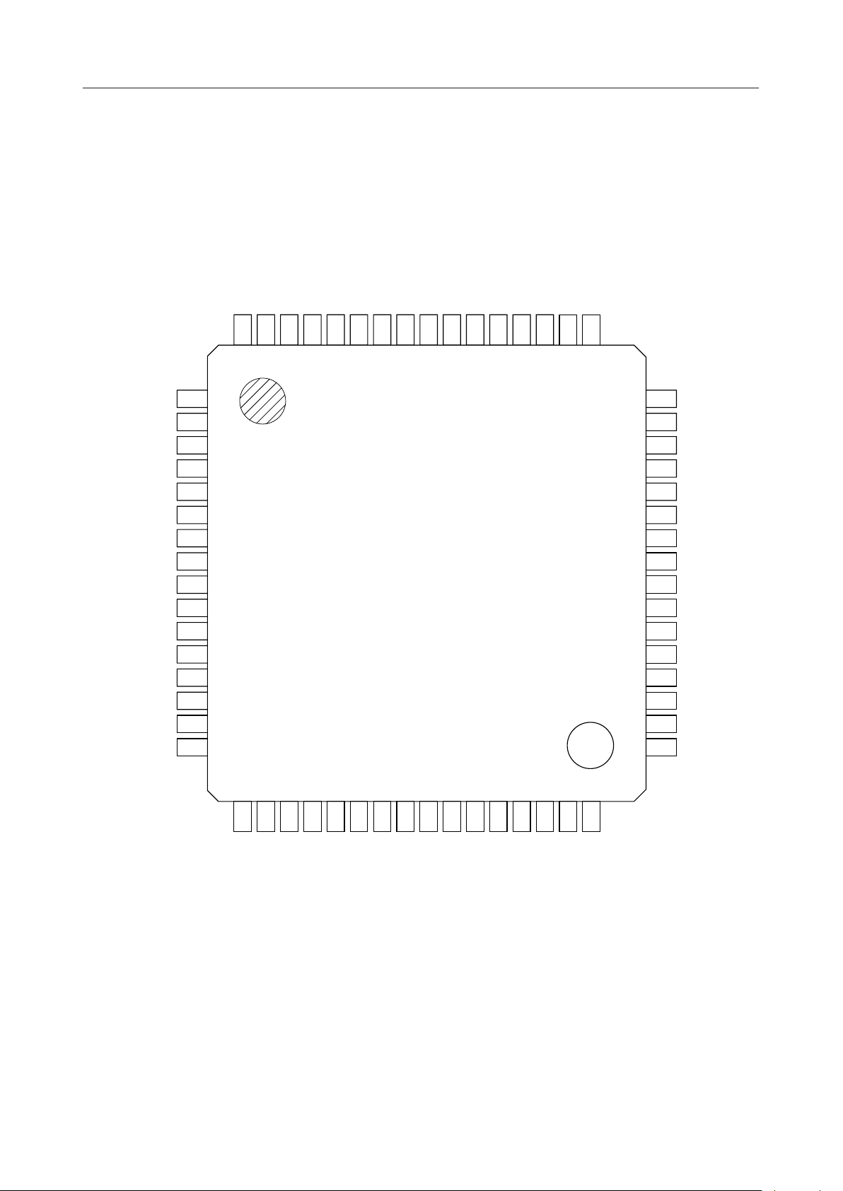
PIN CONFIGURATION (TOP VIEW) (continued)
P0.0/INT0
P0.1/INT1
P0.2/INT2
P0.3/INT3
P1.0/TM0CAP/TM0OVF
P1.1/TM1CAP/TM1OVF
P1.2/T0CK
P1.3/T1CK
P2.0/TBCCLK
P2.1/HSCLK
P2.2
P2.3
PA.0
PA.1
64
63
62
61
60
59
58
57
56
55
54
53
52
51
P9.3
50
P9.2
49
PA.2
PA.3
P3.0/RXD
P3.1/TXC
P3.2/RXC
P3.3/TXD
P4.0
P4.1
P4.2
P4.3
P5.0
P5.1
P5.2
P5.3
P6.0
P6.1
10
11
12
13
14
15
16
1
2
3
4
5
6
7
8
9
48
47
46
45
44
43
42
41
40
39
38
37
36
35
34
33
P9.1
P9.0
MD
RESETB
OSC1
OSC0
V
SS
TST2B
TST1B
XT1
XT0
V
DDL
CB2
CB1
(NC)
(NC)
17
P6.2
P6.3
P7.0/CMPIN
P8.0
P7.3/LDIN1
P7.2/LDIN0
P7.1/CMPREF
P8.1
P8.2
P8.3
DDI
V
SS
DD
V
V
DDH
V
31
(NC)
30
29
28
27
26
25
24
23
22
21
20
19
18
64-Pin Plastic TQFP
Note: Pins marked as (NC) are no-connection pins which are left open.
32
(NC)
6/29
Page 7
¡ Semiconductor ML63512A/63514A
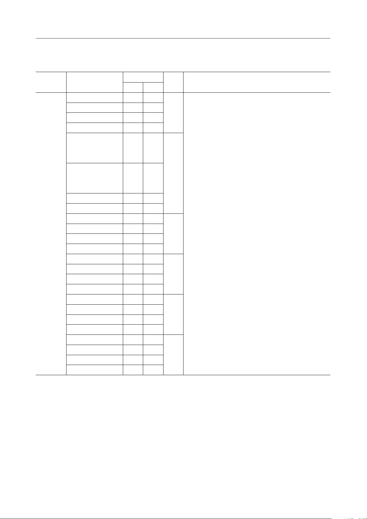
PIN DESCRIPTIONS
The basic functions of each pin of the ML63512A/63514A are described in Table 1.
A symbol with a slash (/) denotes a pin that has a secondary function.
Refer to Table 2 for secondary functions.
For type, "—" denotes a power supply pin, "I" an input pin, "O" an output pin, and "I/O" an inputoutput pin.
For pin, "TB" denotes a 48-pin flat package (48TQFP), and "TP" a 64-pin flat package (64TQFP).
Table 1 Pin Descriptions (Basic Functions)
Function Symbol
Pin
Power
V
V
V
V
DD
SS
DDI
DDL
TB
23 —
22, 32 —
21 —
27 —
TP
29
28, 42
27
37
Supply
V
DDH
24 —
CB1 25 —
CB2 26 —
XT0 28 I
XT1 29 O
30
35
36
38
39
Oscillation
OSC0 33 I
OSC1 34 O
TST1B 30 I
43
44
40
Test
TST2B 31 I
Reset RESETB 35 I
41
45
Type
Description
Positive power supply
Negative power supply
Positive power supply pin for external interface (PORT8 supply)
Positive power supply pin for internal logic (internally generated).
A capacitor C
(0.1 mF) should be connected between this pin and VSS.
l
Voltage multiplier pin for power supply backup (internally generated).
A capacitor C
(1.0 mF) should be connected between this pin and VSS.
h
Pins to connect a capacitor for voltage multiplier.
A capacitor (1.0 mF) should be connected between CB1 and CB2.
Low-speed clock oscillation pins.
Crystal oscillation or RC oscillation is selected by the mask option.
If crystal oscillation is selected, connect a crystal between XT0 and
XT1, and connect capacitor (C
) between XT0 and VSS.
G
If RC oscillation is selected, connect external oscillation resistor
) between XT0 and XT1.
(R
CRL
High-speed clock oscillation pins.
Ceramic oscillation or RC oscillation is selected by the mask option.
If ceramic oscillation is selected, connect a ceramic resonator
between OSC0 and OSC1, and connect capacitor (C
OSC0 and V
, OSC1 and VSS.
SS
, CL1) between
L0
If RC oscillation is selected, connect external oscillation resistor
) between OSC0 and OSC1.
(R
CRH
Input pins for testing.
A pull-up resistor is internally connected to these pins.
Reset input pin.
Setting this pin to "L" level puts this device into a reset state.
Then, setting this pin to "H" level starts executing an instruction
from address 0000H.
An internal or external pull-up resistor is selected by mask option.
Melody MD 36 O
46
Melody output pin (non-inverted output)
7/29
Page 8
¡ Semiconductor ML63512A/63514A
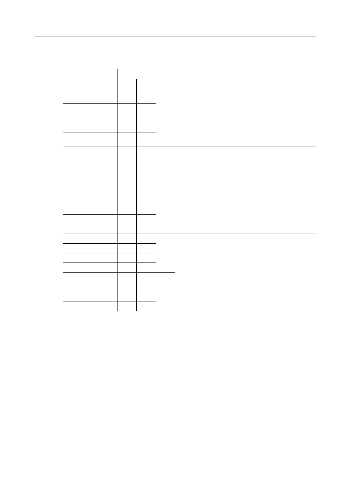
Table 1 Pin Descriptions (Basic Functions) (continued)
Function Symbol
P0.0/INT0 37
P0.1/INT1 38 52
P0.2/INT2 39 53
P0.3/INT3 40 54
P1.0/
TM0CAP/
TM0OVF
P1.1/
TM1CAP/
TM1OVF
P1.2/T0CK 43 57
P1.3/T1CK 44 58
P2.0/TBCCLK 45 59
P2.1/HSCLK 46 60
P2.2 47 61
P2.3 48 62
P3.0/RXD 1 3
P3.1/TXC 2 4
P3.2/RXC 3 5
P3.3/TXD 4 6
P4.0 5 7
P4.1 6 8
P4.2 7 9
P4.3 8 10
P5.0 9 11
P5.1 10 12
P5.2 11 13
P5.3 12 14
Pin
TB
41 55
42 56
TP
51
Type
I/O
I/O
I/OPort
I/O
I/O
I/O
Description
4-bit input-output ports.
In input mode, pull-up resistor input or high-impedance
input is selectable for each bit.
In output mode, N-channel open drain output or CMOS
output is selectable for each bit.
8/29
Page 9
¡ Semiconductor ML63512A/63514A
Table 1 Pin Descriptions (Basic Functions) (continued)
Function Symbol
P6.0 —
P6.1 — 16
P6.2 — 17
P6.3 — 18
P7.0/CMPIN 13 19
P7.1/CMPREF 14 20
P7.2/LDIN0 15 21
P7.3/LDIN1 16 22
Port
P8.0 17 23
P8.1 18 24
P8.2 19 25
P8.3 20 26
P9.0 — 47
P9.1 — 48
P9.2 — 49
P9.3 — 50
PA.0 — 63
PA.1 — 64
PA.2 — 1
PA.3 — 2
TB
Pin
TP
15
Type
I/O
I
O
I/O
I/O
Description
4-bit input-output port.
In input mode, pull-up resistor input or high-impedance
input is selectable for each bit.
In output mode, N-channel open drain output or CMOS
output is selectable for each bit.
Note that these pins are available for only a 64-pin package.
4-bit input port.
Pull-up resistor input or high-impedance input is selectable
for each bit.
4-bit output port.
N-channel open drain output.
4-bit input-output ports.
In input mode, pull-up resistor input or high-impedance
input is selectable for each bit.
In output mode, N-channel open drain output or CMOS
output is selectable for each bit.
Note that these pins are available for only a 64-pin package.
9/29
Page 10

¡ Semiconductor ML63512A/63514A
Table 2 shows the secondary functions of each pin of the ML63512A/63514A.
Table 2 Pin Descriptions (Secondary Functions)
Function Symbol Type Description
P0.0/INT0 37 51
P0.1/INT1 38 52
External
Interrupt
P0.2/INT2 39 53
P0.3/INT3 40 54
Capture
Timer
Oscillation
Output
Serial
Port
Comparator
Level
Detector
P1.0/TM0CAP 41 55 I Timer 0 (TM0) capture trigger input pin.
P1.1/TM1CAP 42 56 I Timer 1 (TM1) capture trigger input pin.
P1.0/TM0OVF 41 55 O Timer 0 (TM0) overflow flag output pin.
P1.1/TM1OVF 42 56 O Timer 1 (TM1) overflow flag output pin.
P1.2/T0CK 43 57 I Timer 0 (TM0) external clock input pin.
P1.3/T1CK 44 58 I Timer 1 (TM1) external clock input pin.
P2.0/TBCCLK 45 59 O Low-speed oscillation clock output pin.
P2.1/HSCLK 46 60 O High-speed oscillation clock output pin.
P3.0/RXD 1 3 I Serial port receive data input pin.
P3.1/TXC 2 4 I/O
P3.2/RXC 3 5 I/O
P3.3/TXD 4 6 O Serial port transmit data output pin.
P7.0/CMPIN 13 19 I Comparator analog input pin.
P7.1/CMPREF 14 20 I Comparator reference voltage input pin.
P7.2/LDIN0 15 21 I Level detector analog input pin.
P7.3/LDIN1 16 22 I Level detector analog input pin.
Pin
TB TP
External 0 interrupt input pin.
Edge detection can be selected from one of a rising edge,
I
a falling edge, or both rising and falling edges.
External 1 interrupt input pin.
Edge detection can be selected from one of a rising edge,
I
a falling edge, or both rising and falling edges.
External 2 interrupt input pin.
Edge detection can be selected from one of a rising edge,
I
a falling edge, or both rising and falling edges.
External 3 interrupt input pin.
Edge detection can be selected from one of a rising edge,
I
a falling edge, or both rising and falling edges.
Sync serial port clock input-output pin.
Transmit sync clock input-output pin when a serial port is used
synchronously.
Transmit clock output when this device is used as a master processor.
Transmit clock input when this device is used as a slave processor.
Sync serial port clock input-output pin.
Receive sync clock input-output pin when a serial port is used
synchronously.
Receive clock output when this device is used as a master processor.
Receive clock input when this device is used as a slave processor.
10/29
Page 11

¡ Semiconductor ML63512A/63514A
ABSOLUTE MAXIMUM RATINGS
(V
= 0 V)
SS
Parameter Symbol Condition Rating Unit
Power Supply Voltage 1 V
V
OUT1
OUT2
OUT3
T
DD
DDI
DDH
DDL
IN1
IN2
STG
D
DDI
DDI
DDH
–0.3 to +5.8Ta = 25°C V
–0.3 to +5.8Power Supply Voltage 2 Ta = 25°CV
–0.3 to +5.8Power Supply Voltage 3 Ta = 25°C
–0.3 to +5.8Power Supply Voltage 4 Ta = 25°CV
–0.3 to V
Input, Ta = 25°CV
–0.3 to V
–0.3 to V
Output, Ta = 25°CV
Output, Ta = 25°CV
–0.3 to V
–0.3 to V
DD
DDI
DD
DDI
DDH
+ 0.3Input Voltage 1 VDD Input, Ta = 25°CV
+ 0.3Input Voltage 2 V
+ 0.3Output Voltage 1 VDD Output, Ta = 25°CV
+ 0.3Output Voltage 2 V
+ 0.3Output Voltage 3 V
–55 to +150Storage Temperature —
60Power Dissipation Ta = 25°CP
V
V
V
V
V
V
V
V
°C
mW
11/29
Page 12

¡ Semiconductor ML63512A/63514A
RECOMMENDED OPERATING CONDITIONS
• When backup is used
(V
= 0 V)
SS
Parameter Symbol Condition Range Unit
Operating Temperature T
Operating Voltage
Crystal Oscillation Frequency f
Low-Speed RC Oscillator
Frequency
External High-Speed RC
Oscillator Resistance
• When backup is not used
R
V
V
f
op
DD
DDI
XT
CRL
CRH
—
— 0.9 to 1.8 V
—
—
= 1 MW ±10%
CRL
= 0.9 to 1.8 V
DD
–20 to +70 °C
0.9 to 3.5 V
30 to 80 kHz
32 kHzR
100 to 300 kWV
Parameter Symbol Condition Range Unit
Operating Temperature T
Operating Voltage
Crystal Oscillation Frequency f
Low-Speed RC Oscillator
Frequency
External High-Speed RC
Oscillator Resistance
R
Ceramic Oscillation Frequency
V
V
f
f
op
DD
DDI
XT
CRL
CRH
CM
—
— 1.8 to 3.5
When Level detector and
Comparator are not used
—
—
= 1 MW ±10%
CRL
= 1.8 to 5.5 V
DD
= 2.2 to 5.5 V
DD
= 0 V)
(V
SS
–20 to +70 °C
1.8 to 5.5 V
1.8 to 5.5
30 to 80 kHz
32R
15 to 300V
kHz
kW
300k to 1MV
200k to 2MVDD = 2.7 to 5.5 V
Hz
12/29
Page 13

¡ Semiconductor ML63512A/63514A
ELECTRICAL CHARACTERISTICS
DC Characteristics
• When backup is used
(VDD = V
= 1.5 V, VSS = 0 V, Ta = –20 to +70°C unless otherwise specified)
DDI
Parameter Symbol Condition
CPU is in HALT state
Supply Current 1
I
High-speed oscillation stop
DD1
Level detector stop
CPU operating
Supply Current 2
I
High-speed oscillation stop
DD2
Level detector stop
CPU operating at low speed
I
DD3
High-speed oscillation stop
Level detector active
(for a soft duty of about 3%)
CPU operating at high speed
DD4
High-speed RC oscillation
R
= 100 kW
CRH
• When backup is not used
Ta = 25°C
Ta = –20 to +50°C
Ta = –20 to +70°C
Ta = 25°C
Ta = –20 to +50°C
Ta = –20 to +70°C
4.8
—
—
12.0
—
—
5.3
5.3
5.3
13.0
13.0
13.0
Max.Typ.Min.
5.8
9.0
15.0
14.0
16.0
24.0
35.010.0—Supply Current 3
750.0550.0—Supply Current 4 I
Unit
mA
mA
mA
mA
Mea-
suring
Circuit
1
(VDD = V
= 3.0 V, VSS = 0 V, Ta = –20 to +70°C unless otherwise specified)
DDI
Parameter Symbol Condition
CPU is in HALT state
Supply Current 1
I
High-speed oscillation stop
DD1
Level detector stop
CPU operating
Supply Current 2
I
High-speed oscillation stop
DD2
Level detector stop
CPU operating at low speed
I
DD3
High-speed oscillation stop
Level detector active
(for a soft duty of about 3%)
CPU operating at high speed
DD4
High-speed RC oscillation
R
= 100 kW
CRH
CPU operating at high speed
DD5
High-speed ceramic oscillation
(ceramic oscillation, 2 MHz)
Ta = 25°C
Ta = –20 to +50°C
Ta = –20 to +70°C
Ta = 25°C
Ta = –20 to +50°C
Ta = –20 to +70°C
2.1
—
—
5.0
—
—
2.4
2.4
2.4
6.0
6.0
6.0
Max.Typ.Min.
550.0410.0—Supply Current 4 I
1000.0850.0—Supply Current 5 I
2.7
7.0
10.0
7.0
9.0
15.0
25.06.0—Supply Current 3
Unit
mA
mA
mA
mA
mA
Mea-
suring
Circuit
1
13/29
Page 14

¡ Semiconductor ML63512A/63514A
DC Characteristics (continued)
Parameter
(Pin Name)
Voltage
V
DDH
V
Voltage
DDL
Crystal Oscillation Start
Voltage
Crystal Oscillation Hold
Voltage
External Crystal Oscillator
Capacitance
Internal Crystal Oscillator
Capacitance
Internal Low-Speed RC
Oscillator Capacitance
Internal High-Speed RC
Oscillator Capacitance
Input Pin Capacitance
(P0.0 to P0.3)
(P1.0 to P1.3)
···
(P7.0 to P7.3)
(P9.0 to P9.3)
(PA.0 to PA.3)
(VDD = V
= 1.5 V, VSS = 0 V, Ta = –20 to +70°C unless otherwise specified)
DDI
Symbol Condition Typ.Min. Max.
High-speed clock stop
2.8 — 3.0
= 1.5 V
V
V
DDH
High-speed clock oscillation
DD
2.0 — —
(RC oscillation, R
= 100 kW)
CRH
High-speed clock stop 1.0 1.5 2.0
V
V
V
HOLD
C
C
C
DDL
STA
C
C
G
D
XT
OS
IN
High-speed clock oscillation 2.0 — 2.7
Oscillation start time: within 5 seconds 1.2 — —
— 0.9 — —
— 5.0 — 25.0
— 20.0 25.0 30.0
— 10.0 15.0 20.0
— 8.0 12.0 16.0
— — — 5.0
Unit
V
V
V
V
V
V
pF
pF
pF
pF
pF
Mea-
suring
Circuit
1
14/29
Page 15

¡ Semiconductor ML63512A/63514A
DC Characteristics (continued)
Parameter
(Pin Name)
Output Current 1
(P0.0 to P0.3)
(P1.0 to P1.3)
···
(P6.0 to P6.3)
(P9.0 to P9.3)
(PA.0 to PA.3)
(MD)
Output Current 2
(P8.0 to P8.3)
Output Current 3
(OSC1)
Output Leakage
(P0.0 to P0.3)
(P1.0 to P1.3)
···
(P6.0 to P6.3)
(P8.0 to P8.3)
(P9.0 to P9.3)
(PA.0 to PA.3)
(VDD = V
= 1.5 V, VSS = 0 V, Ta = –20 to +70°C unless otherwise specified)
DDI
Symbol Condition Typ.Min. Max.
–0.2–1.3–2.5
–1.0–3.5–6.0
–1.5–5.0–8.5
2.51.30.2
6.03.01.0
8.53.71.5
1.0——
14.07.53.0
20.012.06.0
28.015.08.0
–0.2–1.5–2.5
–0.5–1.8–3.5
2.51.50.2
3.51.80.5
–60–160–300
–100–240–400
30017060
400210100
1.0——I
——–1.0I
I
OH1
I
OL1
I
OH2Z
I
OL2
I
OH3R
I
OL3R
I
OH3C
I
OL3C
OOHVOH
OOLVOL
= VDD – 0.5 V
V
OH1
V
= 0.5 V
OL1
= V
V
OH2
V
= 0.5 V
OL2
= V
V
OH3R
= 0.5 V
V
OL3R
= V
V
OH3C
= 0.5 V
V
OL3C
= V
= V
DD
SS
DD
DDH
DDH
– 0.5 V
– 0.5 V
VDD = 1.5 V
= 3.0 V
V
DD
V
= 5.0 V
DD
VDD = 1.5 V
= 3.0 V
V
DD
V
= 5.0 V
DD
V
= 1.5 V
DDI
V
= 3.0 V
DDI
V
= 5.0 V
DDI
VDD = V
V
VDD = V
V
VDD = V
V
VDD = V
V
DD
DD
DD
DD
= V
= V
= V
= V
DDH
DDH
DDH
DDH
DDH
DDH
DDH
DDH
= 3.0 V
= 5.0 V
= 3.0 V
= 5.0 V
= 3.0 V
= 5.0 V
= 3.0 V
= 5.0 V
Unit
mA
mA
mA
mA
mA
mA
mA
mA
mA
mA
mA
mA
mA
mA
mA
mA
mA
mA
mA
mA
Mea-
suring
Circuit
2
15/29
Page 16

¡ Semiconductor ML63512A/63514A
DC Characteristics (continued)
Parameter
(Pin Name)
Input Current 1
(P0.0 to P0.3)
(P1.0 to P1.3)
···
(P7.0 to P7.3)
(P9.0 to P9.3)
(PA.0 to PA.3)
Input Current 2
(RESETB)
Input Current 3
(OSC0)
Input Current 4
(TST1B, TST2B)
(VDD = V
= 1.5 V, VSS = 0 V, Ta = –20 to +70°C unless otherwise specified)
DDI
Symbol Condition
V
I
IH1U
= VDD (when pulled up)
IH1
VDD = 1.5 V
V
= V
IL1
IH2
SS
= V
(in a high-impedance state) mA
DD
= V
(in a high-impedance state) mA
SS
= V
DD
V
DD
V
DD
I
IL1U
(when pulled up)
I
IH1ZVIH1
I
IL1ZVIL1
I
V
IH2
VDD = 1.5 V
V
= V
IL2
I
IL2
(when pulled up)
SS
VDD = 3.0 V
VDD = 5.0 V
V
I
IL3
IH3RVIH3
IL3RVIL3
I
IH4
IL3
(when pulled up)
V
IH4
= V
= V
= V
= V
SS
DDH
SS
DD
V
DD
V
DD
VDD = 1.5 V
V
= V
IL4
I
IL4
(when pulled up)
SS
V
DD
V
DD
= 3.0 V
= 5.0 V
= V
DDH
= V
DDH
= 3.0 V
= 5.0 V
= 3.0 V
= 5.0 V
–1320.0
Unit
Max.Typ.Min.
1.0——
mA
–1.0–4.0–8.0
mA
–10.0–30.0–60.0 mA
–23.0–90.0–150.0 mA
1.0——
——–1.0
1.0—— mA
–2.0–20.0–45.0 mA
–30.0–120.0–260.0 mA
–70.0–300.0–870.0
–30.0–170.0–350.0
mA
mA
–200.0–450.0–750.0 mA
mA
1.0——I
mA
——–1.0I
0.1—— mA
–10.0–60.0–120.0 mA
–100.0–350.0–600.0
–220.0–770.0
mA
mA
Mea-
suring
Circuit
3
16/29
Page 17

¡ Semiconductor ML63512A/63514A
DC Characteristics (continued)
Parameter
(Pin Name)
Input Voltage 1
(P0.0 to P0.3)
(P1.0 to P1.3)
······
(P7.0 to P7.3)
(P9.0 to P9.3)
(PA.0 to PA.3)
Input Voltage 2
(OSC0)
Input Voltage 3
(RESETB)
(TST1B, TST2B)
Hysteresis Width
(P0.0 to P0.3)
(P1.0 to P1.3)
(VDD = V
= 1.5 V, VSS = 0 V, Ta = –20 to +70°C unless otherwise specified)
DDI
Symbol Condition
= 1.5 V
V
DD
V
IH1
V
IL1
V
IH2
V
IL2
V
IH3
V
IL3
V
DD
V
DD
V
DD
V
DD
V
DD
V
DD
V
DD
V
DD
V
DD
V
DD
V
DD
V
DD
V
DD
V
DD
V
DD
V
DD
= 3.0 V
= 5.0 V
= 1.5 V
= 3.0 V
= 5.0 V
= V
DDH
= V
DDH
= V
DDH
= V
DDH
= 1.5 V
= 3.0 V
= 5.0 V
= 1.5 V
= 3.0 V
= 5.0 V
= 1.5 V
= 3.0 V
= 5.0 V
= 3.0 V
= 5.0 V
Max.Typ.Min.
1.5—1.2
3.0—2.4
5.0—4.0 V
0.3—0.0
0.6—0.0 V
1.0—0.0 V
3.0—2.4
5.0—4.0
0.6—0.0
1.0—0.0 V
1.50—1.35
3.0—2.4 V
5.0—4.0 V
0.15—0.00
0.6—0.0 V
1.0—0.0 V
0.300.100.05
Unit
V
V
V
V
V
V
V
V
V
Mea-
suring
Circuit
4
(P7.0 to P7.3)
(P9.0 to P9.3)
(PA.0 to PA.3)
(RESETB)
(TST1B, TST2B)
V
T
V
DD
V
DD
= 3.0 V
= 5.0 V
1.00.50.2 V
1.501.000.25 V
17/29
Page 18

¡ Semiconductor ML63512A/63514A
Hysteresis width
V
Input Signal
T
V
DD
V
SS
Internal Signal V
DDL
V
SS
18/29
Page 19

¡ Semiconductor ML63512A/63514A
Measuring circuit 1
*1
*2
*1
q
w
e
r
RC oscillator
XT0
XT1
OSC0
OSC1
CB1
C
b12
CB2
V
SS
V
DD
V
A
DDI
V
DDH
C
h
V
DDL
C
l
V
C
G
C
b12
C
l
C
O
Ceramic Resonator
V
: 15 pF
: 1 mF
, C
h
: 0.1 mF
: 12 pF
: CSA2.00MG (2 MHz)
CSB1000J (1 MHz)
(Murata MFG.-make)
C
L0
C
L1
: 30 pF
: 30 pF
*2
RC oscillator
R
CRL
Crystal oscillator
C
G
q
w
q
w
R
CRH
Ceramic oscillator
C
L0
C
Ceramic resonator
L1
e
r
e
r
19/29
Page 20

¡ Semiconductor ML63512A/63514A
p
Measuring circuit 2
*4
V
IH
*3
V
IL
Measuring circuit 3
*5
INPUT OUTPUT
V
SS
V
DD
V
DDI
V
DDHVDDL
*3 Input logic circuit to determine the specified measuring conditions.
*4 Measured at the s
ecified output pins.
A
A
INPUT OUTPUT
V
SS
V
DD
V
DDI
V
DDHVDDL
20/29
Page 21

¡ Semiconductor ML63512A/63514A
Measuring circuit 4
V
IH
*5
V
IL
INPUT OUTPUT
V
SS
V
DD
V
DDI
V
DDH
V
DDL
Waveform
Monitoring
*5 Measured at the specified input pins.
21/29
Page 22

¡ Semiconductor ML63512A/63514A
AC Characteristics (Serial Interface, Serial Port)
(VDD = 0.9 to 5.5 V, V
= 1.8 to 5.5 V, VSS = 0 V, V
DDH
otherwise specified)
(1) Synchronous Communication
Parameter Symbol Condition Unit
t
f
r
TXC/RXC Input "L" Level
Pulse Width
TXC/RXC Input "H" Level
Pulse Width
TXC/RXC Output Cycle Time
t
CWL
t
CWH
CYC
t
CYC1(O)
CYC2(O)
DDR
DS
DH
= 0.9 to 5.5 V, Ta = –20 to +70°C unless
DDI
Max.Typ.Min.
— ms— 1.0
— ms— 1.0
— ms——
— ms——
— ms——
CPU operating at 32.768 kHz ms30.5 —
—TXC/RXC Input Fall Time
—TXC/RXC Input Rise Time t
0.8
0.8
2.0TXC/RXC Input Cycle Time t
—
CPU operating at 2 MHz
= V
V
DD
= 2.7 to 5.5 V
DDH
Output load capacitance 10 pF ms— 0.4
— ms——
— ms——
—t
—TXD Output Delay Time t
0.5RXD Input Setup Time t
0.8RXD Input Hold Time t
ms0.5 —
Synchronous communication timing
("H" level = 4.0 V, "L" level = 1.0 V)
t
CYC
TXC (P3.1)/
RXC (P3.2)
t
DDR
TXD (P3.3)
t
DS
RXD (P3.0)
VDD (5.0 V)
V
t
r
t
CWH
t
DDR
t
f
t
CWL
SS
VDD (5.0 V)
V
SS
t
DH
t
DS
VDD (5.0 V)
V
SS
22/29
Page 23

¡ Semiconductor ML63512A/63514A
(2) UART Communication
Parameter Symbol Condition Unit
Transmit Baud Rate
T
BRT
BRT
UART communication timing
("H" level = 4.0 V, "L" level = 1.0 V)
TXD (P3.3)
RXD (P3.0)
Max.Typ.Min.
T
= 1/f
BRT
TCR = 1/f
BRT
f
: Baud rates (2TBCCLK, TBCCLK, 1/2TBCCLK, Timer 0/1 overflow)
BRT
T
= 1/f
BRT
BRT
OSC
BRT
T
BRT–TCR
R
BRT
BRT
¥0.97Receive Baud Rate R
BRT
T
BRT+TCR
R
BRT
¥1.03R
VDD (5.0 V)
V
SS
R
BRT
VDD (5.0 V)
V
SS
sT
sR
23/29
Page 24

¡ Semiconductor ML63512A/63514A
AC Characteristics
(VDD = V
= 0.9 to 5.5 V, VSS = 0 V, Ta = –20 to + 70°C unless otherwise specified)
DDI
Parameter Symbol Condition Unit
External Interrupt Enable
Pulse Width (Rising Edge)
External Interrupt Enable
Pulse Width (Falling Edge)
External Interrupt Disable
Time
AC characteristics timing
P0.0 to P0.3
(Interrupt on the rising edge)
P0.0 to P0.3
t
t
t
NUL
WH
WL
—ns——
—ns——
Interrupt enable, MIE = 1
CPU operating under
the NOP instruction
System clock: 32.768 kHz
t
WH
t
NUL
20
20
13.0
Max.Typ.Min.
ms— 65.1
(Interrupt on the falling edge)
P0.0 to P0.3
(Interrupt on both rising and falling edges)
t
WL
t
NUL
t
NUL
24/29
Page 25

¡ Semiconductor ML63512A/63514A
Comparator Electrical Characteristics
(V
= 0.9 V, VSS = 0 V, Ta = –20 to +70°C)
DD
Parameter Symbol Condition Min. Typ. Max. Unit
Remarks
Comparator Offset
Voltage
V
coff
— — — 30 mV
Comparator Input
Voltage
Comparator Conversion
Time
Comparator Supply
Current
V
cin
T
I
DDCMP
I
DSCMP
—V
System clock: 32.768 kHz — 183 — ms
C
SS
Comparator operating — 30 90 mA
Comparator stopped — — 0.1 mA
—VDDV
CMPIN
CMPREF
Conceptual diagram of comparator supply current
The conceptual diagram of the comparator supply current I
I
DD
(VSS)
[mA]
I
DDCMP
I
DSCMP
Sampling reference voltage Comparing
Level detector operatingLevel detector stopped Level detector stopped
DDCMP
and I
reference
voltage with
input voltage
DSCMP
is shown below.
t [ms]
25/29
Page 26

¡ Semiconductor ML63512A/63514A
Level Detector Electrical Characteristics
= 0.9 V, VSS = 0 V, Ta = –20 to +70°C)
(V
DD
Parameter Symbol Condition Min. Typ. Max. Unit
Remarks
Level Detector Input
Voltage
Level Detector Conversion
Time
Level Dtector Supply
Current
V
T
I
DDLD
I
DSLD
LD
System clock: 32.768 kHz — 183 — ms
C
— V
SS
Level detector operating — 80 130 mA
Level detector stopped — — 0.1 mA
—VDDV
LDIN0, 1
Conceptual diagram of level detector supply current
The conceptual diagram of the level detector supply current I
I
DD
(VSS)
[mA]
I
DDLD
I
DSLD
Sampling reference voltage Comparing
voltage with
input voltage
Level detector operatingLevel detector stopped Level detector stopped
DDLD
reference
and I
is shown below.
DSLD
t [ms]
26/29
Page 27

¡ Semiconductor ML63512A/63514A
Level Detector Input Levels and Output Codes
(VDD = 0.9 to 1.8 V: when backup is used, VDD = 1.8 to 3.5 V: when backup is not used;
V
= 0 V, Ta = –20 to +70°C)
SS
Input Level [V]
Min. Max.
1440/1500 ¥ V
1306/1500 ¥ V
1190/1500 ¥ V
1074/1500 ¥ V
958/1500 ¥ V
842/1500 ¥ V
726/1500 ¥ V
610/1500 ¥ V
494/1500 ¥ V
378/1500 ¥ V
262/1500 ¥ V
146/1500 ¥ V
V
DD
DD
DD
DD
DD
DD
DD
DD
DD
DD
DD
DD
SS
V
DD
1366/1500 ¥ V
1250/1500 ¥ V
1134/1500 ¥ V
1018/1500 ¥ V
902/1500 ¥ V
786/1500 ¥ V
670/1500 ¥ V
554/1500 ¥ V
438/1500 ¥ V
322/1500 ¥ V
206/1500 ¥ V
88/1500 ¥ V
DD
DD
DD
DD
DD
DD
DD
DD
DD
DD
DD
DD
Level Detector
Operation State
OFF state
ON state
bit 3
1
1
1
1
1
0
0
0
0
0
0
0
0
LDOUT
bit 2
1
0
0
0
0
1
1
1
1
0
0
0
0
bit 1
1
1
1
0
0
1
1
0
0
1
1
0
0
bit 0
1
1
0
1
0
1
0
1
0
1
0
1
0
27/29
Page 28

¡ Semiconductor ML63512A/63514A
PACKAGE DIMENSIONS
(Unit : mm)
TQFP48-P-0707-0.50-K
Mirror finish
Package material
Lead frame material
Pin treatment
Solder plate thickness
Package weight (g)
Epoxy resin
42 alloy
Solder plating
5 mm or more
0.13 TYP.
Notes for Mounting the Surface Mount Type Package
The SOP, QFP, TSOP, TQFP, LQFP, SOJ, QFJ (PLCC), SHP, and BGA are surface mount type
packages, which are very susceptible to heat in reflow mounting and humidity absorbed in
storage. Therefore, before you perform reflow mounting, contact Oki’s responsible sales person
on the product name, package name, pin number, package code and desired mounting conditions
(reflow method, temperature and times).
28/29
Page 29

¡ Semiconductor ML63512A/63514A
(Unit : mm)
TQFP64-P-1010-0.50-K
Mirror finish
Package material
Lead frame material
Pin treatment
Solder plate thickness
Package weight (g)
Epoxy resin
42 alloy
Solder plating
5 mm or more
0.26 TYP.
Notes for Mounting the Surface Mount Type Package
The SOP, QFP, TSOP, TQFP, LQFP, SOJ, QFJ (PLCC), SHP, and BGA are surface mount type
packages, which are very susceptible to heat in reflow mounting and humidity absorbed in
storage. Therefore, before you perform reflow mounting, contact Oki’s responsible sales person
on the product name, package name, pin number, package code and desired mounting conditions
(reflow method, temperature and times).
29/29
Page 30

E2Y0002-29-62
NOTICE
1. The information contained herein can change without notice owing to product and/or
technical improvements. Before using the product, please make sure that the information
being referred to is up-to-date.
2. The outline of action and examples for application circuits described herein have been
chosen as an explanation for the standard action and performance of the product. When
planning to use the product, please ensure that the external conditions are reflected in the
actual circuit, assembly, and program designs.
3. When designing your product, please use our product below the specified maximum
ratings and within the specified operating ranges including, but not limited to, operating
voltage, power dissipation, and operating temperature.
4. Oki assumes no responsibility or liability whatsoever for any failure or unusual or
unexpected operation resulting from misuse, neglect, improper installation, repair, alteration
or accident, improper handling, or unusual physical or electrical stress including, but not
limited to, exposure to parameters beyond the specified maximum ratings or operation
outside the specified operating range.
5. Neither indemnity against nor license of a third party’s industrial and intellectual property
right, etc. is granted by us in connection with the use of the product and/or the information
and drawings contained herein. No responsibility is assumed by us for any infringement
of a third party’s right which may result from the use thereof.
6. The products listed in this document are intended for use in general electronics equipment
for commercial applications (e.g., office automation, communication equipment,
measurement equipment, consumer electronics, etc.). These products are not authorized
for use in any system or application that requires special or enhanced quality and reliability
characteristics nor in any system or application where the failure of such system or
application may result in the loss or damage of property, or death or injury to humans.
Such applications include, but are not limited to, traffic and automotive equipment, safety
devices, aerospace equipment, nuclear power control, medical equipment, and life-support
systems.
7. Certain products in this document may need government approval before they can be
exported to particular countries. The purchaser assumes the responsibility of determining
the legality of export of these products and will take appropriate and necessary steps at their
own expense for these.
8. No part of the contents contained herein may be reprinted or reproduced without our prior
permission.
9. MS-DOS is a registered trademark of Microsoft Corporation.
Copyright 1999 Oki Electric Industry Co., Ltd.
Printed in Japan
 Loading...