

Page 1
July 1999
ML4903
High Current Synchronous Buck Controller
GENERAL DESCRIPTION
The ML4903 high current synchronous buc k controller
provides high efficiency DC/DC conversion to generate
V
for processors such as the Pentium® Pro and Pentium
CCP
II from Intel
®
.
The ML4903 controller, when combined with two external
MOSFETs, generates output voltages between 1.8V and
3.5V from a 12V supply. The output voltage is selected via
an internal 2 chord 4-bit DAC. In the upper range, the
output can be set between 2.1V and 3.5V in 100mV steps.
In the lower range, the output can be set between 1.8V
and 2.05V in 50mV steps. Output currents in excess of
20A can be attained at efficiencies greater than 80%.
The ML4903 can be enabled/disabled via the SHDN pin.
While disabled, the output of the regulator is completely
isolated from the circuit’s input supply. The ML4903
employs fixed-frequency PWM control combined with a
sophisticated control loop enhancement circuit to provide
excellent load transient response.
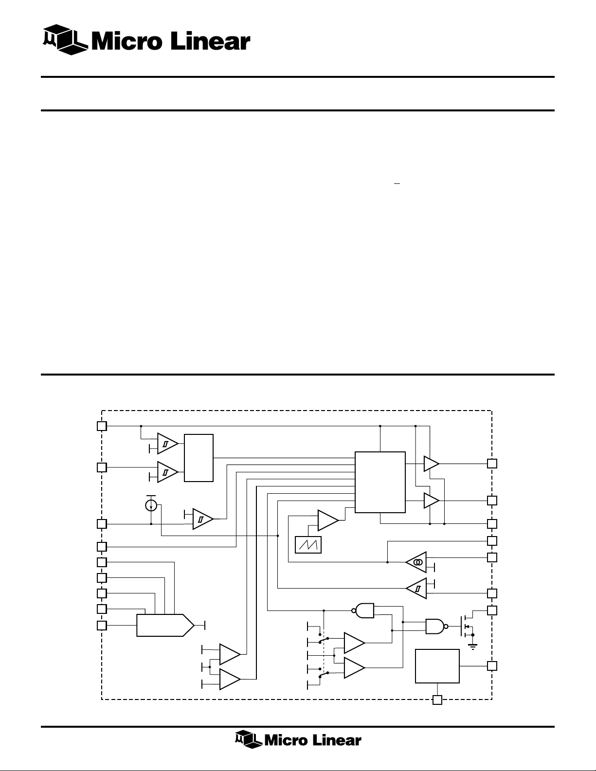
BLOCK DIAGRAM
FEATURES
■ Designed to meet Pentium Pro and Pentium II VRM
power supply requirements
■ DC regulation to +1% maximum
■ Proprietary circuitry provides transient response of ±5%
maximum over a 0A to 14A load range
■ Programmable output voltage (1.8V to 3.5V) is set by
an onboard 2 chord 4-bit D AC
■ Synchronous buck topology for maximum power
conversion efficiency
■ Fixed frequency operation for easier system integration
■ Integrated anti-shootthrough logic, short circuit
protection, shutdown, and UV lockout
V
DD
19
V
CC
18
PROTECT
20
SHDN
6
D0
1
D1
2
D2
3
D3
4
RANGE
5
10.5V
4.4V
30µA
+
–
+
–
5V
3.5V
2 CHORD
4 BIT DAC
V
DAC
V
DAC
UVLO
+ 3%
V
- 3%
P DRV
17
CONTROL
LOGIC
+
–
V
DAC
+
–
FB
+
–
V
V
DAC
V
DAC
DAC
V
DAC
+ 10%
+ 3%
- 10%
- 3%
+
–
200kHz
–
+
+
–
+
V
FB
–
+
–
3.5V
REFERENCE
10
PWR GND
V
DAC
-107mV
PWR GOOD
GND
N DRV
COMP
V
I
SENSE
V
REF
16
15
13
FB
11
12
8
9
1
Page 2

ML4903
PIN CONFIGURATION
ML4903
20-Pin TSSOP (T20)
D0
D1
D2
D3
RANGE
SHDN
NC
PWR GOOD
V
REF
GND
1
2
3
4
5
6
7
8
9
10
PIN DESCRIPTION
PIN NAME FUNCTION
1 D0 LSB input to the DAC which sets the
output voltage
2 D1 Input to the DAC which sets the
output voltage
3 D2 Input to the DAC which sets the
output voltage
20
19
18
17
16
15
14
13
12
11
TOP VIEW
PIN NAME FUNCTION
9V
REF
PROTECT
V
DD
V
CC
P DRV
N DRV
PWR GND
NC
COMP
I
SENSE
V
FB
Bypass connection for the internal
3.5V reference
1 0 GND Analog signal ground
11 V
12 I
FB
SENSE
Output voltage feedback pin
Current sense input
4 D3 MSB input to the DAC which sets the
output voltage
5 RANGE Range selection bit for the 2 chord 4-
bit DAC. Logic 1 sets the range at
2.1V to 3.5V with an LSB of 100mV.
Logic 0 sets the range at 1.8V to
2.05V with an LSB of 50mV.
6 SHDN Grounding this pin shuts down the
regulator
8 PWR GOODThis open drain output goes low
whenever SHDN goes low or when
the output is not within +10% of its
nominal value
1 3 COMP Connection for the compensation and
optional soft-start delay network
15 PWR GND Power ground
1 6 N DRV Synchronous rectifier driver output
1 7 P DRV Buck switch driver output
18 V
CC
Connection point for monitoring the
5V supply to determine the proper
condition of PWR GOOD
19 V
DD
12V power supply input
20 PROTECT Connection for the integrating current
limit network
2
Page 3
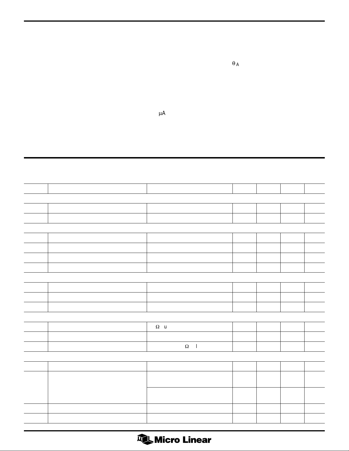
ABSOLUTE MAXIMUM RATINGS
ML4903
Absolute maximum ratings are those values beyond which
the device could be permanently damaged. Absolute
maximum ratings are stress ratings only and functional
device operation is not implied.
V
...........................................................................................
DD
V
..................................................................................................7V
CC
13.5V
Peak Dri ver Output Current.......................................±2A
Voltage...................................... GND - 0.3V to 5.5V
V
FB
I
Voltage.................................. GND - 0.5V to 5.5V
SENSE
All Other Inputs .................... GND - 0.3V to VDD + 0.3V
SHDN Input Current .............................................. 100mA
Junction T emperature.............................................. 150°C
Storage Temperature Range ..................... –65°C to 150°C
Lead Temperature (Soldering, 10 sec) .....................260°C
Thermal Resistance (
qJA).................................... 100°C/W
OPERATING CONDITIONS
T emper ature Range .......................................0°C to 70°C
VDD Range ..............................................11.4V to 12.6V
Range ...............................................4.75V to 5.25V
V
CC
ELECTRICAL CHARACTERISTICS
Unless otherwise specified, VDD = 12V, VCC = SHDN = 5V, TA = Operating Temperature Range (Note 1)
SYMBOL PARAMETER CONDITIONS MIN TYP MAX UNITS
REFERENCE
V
Output Voltage 3.51 3.535 3.56 V
REF
Line Regulation 11V < VDD < 13V 0.5 mV/V
UV LOCKOUT
VDD Start-up Threshold 10.0 10.5 10.8 V
VDD Hysteresis 30 0 450 6 00 mV
VCC Start-up Threshold 4.25 4.4 4.6 V
VCC Hysteresis 30 0 400 50 0 mV
SHUTDOWN
Input Low Voltage 0.8 V
Input High Voltage 2.0 V
Delay to Output 50 ns
POWER GOOD COMPARATOR
Output Voltage in Regulation 5kW pull-up to 5V 4.8 V
Output Voltage out of Regulation VFB < 90% V
Output Voltage in Shutdown SHDN = 0V, 5kW pull-up to 5V 0.4 V
BUCK REGULATOR
Oscillator Frequency 160 200 230 kHz
Duty Cycle Ratio RANGE = 1, V
or >110% V
DAC
= 0V, 80 98 %
DAC (D3-D0) Code = 0100
RANGE = 1, VFB > 3.193V, 0 %
DAC (D3-D0) Code = 0100
FB
DAC
0.4 V
DAC (RANGE, D3-D0) Input Low Voltage 0.8 V
DAC (RANGE, D3-D0) Input High Voltage 2.0 V
3
Page 4
ML4903
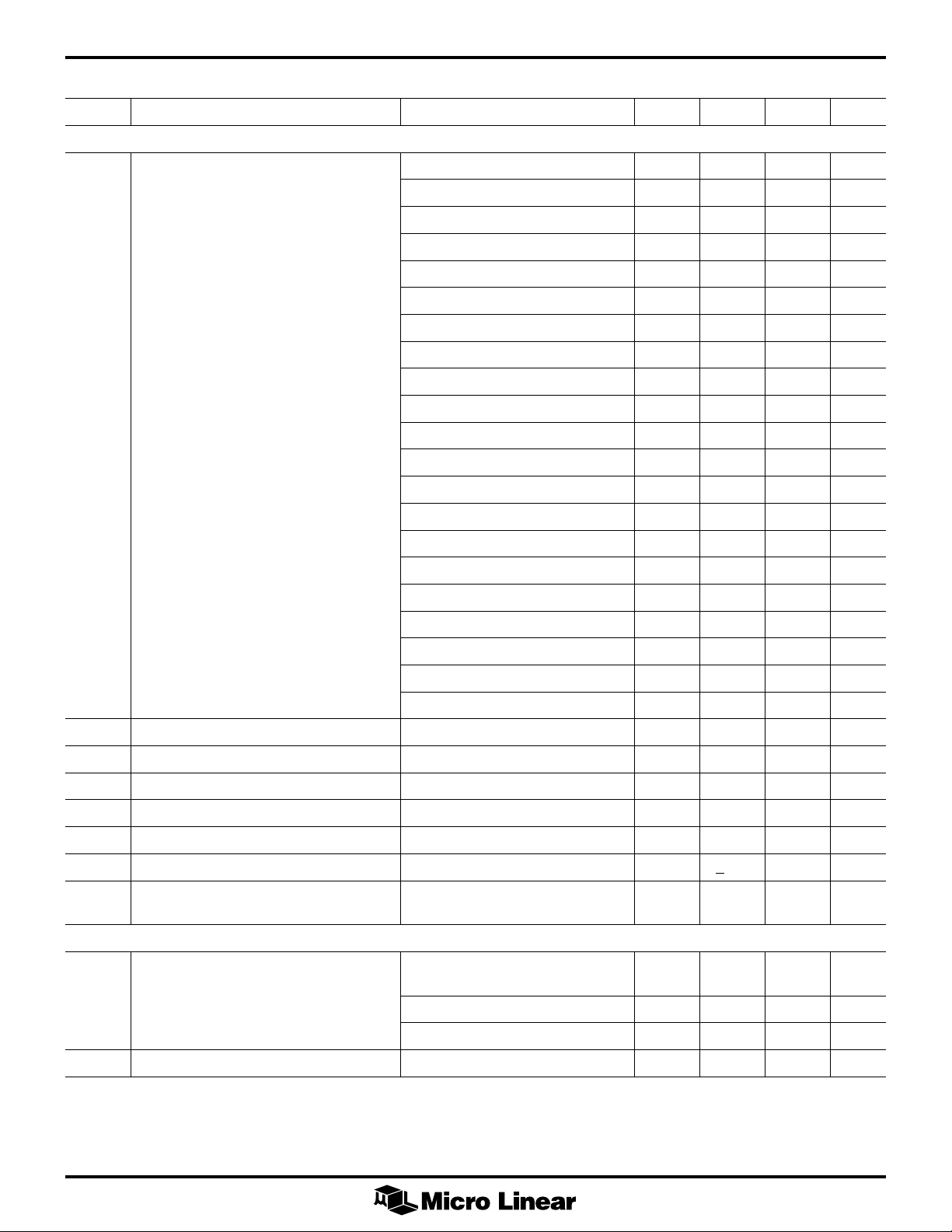
ELECTRICAL CHARACTERISTICS (Continued)
SYMBOL PARAMETER CONDITIONS MIN TYP MAX UNITS
BUCK REGULATOR (Continued)
VFB Threshold Voltage (Note 2) RANGE = 0, (D3-D0) Code = 0000 2.050 2.071 2.092 V
RANGE = 0, (D3-D0) Code = 0001 2.000 2.020 2.04 V
RANGE = 0, (D3-D0) Code = 0010 1.950 1.970 1.989 V
RANGE = 0, (D3-D0) Code = 0011 1.900 1.919 1.938 V
RANGE = 0, (D3-D0) Code = 0100 1.850 1.869 1.887 V
RANGE = 0, (D3-D0) Code = 0101 1.800 1.818 1.836 V
RANGE = 1, (D3-D0) Code = 0000 3.500 3.535 3.570 V
RANGE = 1, (D3-D0) Code = 0001 3.400 3.434 3.468 V
RANGE = 1, (D3-D0) Code = 0010 3.300 3.333 3.366 V
RANGE = 1, (D3-D0) Code = 0011 3.200 3.232 3.264 V
RANGE = 1, (D3-D0) Code = 0100 3.100 3.131 3.162 V
RANGE = 1, (D3-D0) Code = 0101 3.000 3.030 3.060 V
RANGE = 1, (D3-D0) Code = 0110 2.900 2.929 2.958 V
SUPPLY
I
DD
RANGE = 1, (D3-D0) Code = 0111 2.800 2.828 2.856 V
RANGE = 1, (D3-D0) Code = 1000 2.700 2.727 2.754 V
RANGE = 1, (D3-D0) Code = 1001 2.600 2.626 2.652 V
RANGE = 1, (D3-D0) Code = 1010 2.500 2.525 2.550 V
RANGE = 1, (D3-D0) Code = 1011 2.400 2.424 2.448 V
RANGE = 1, (D3-D0) Code = 1100 2.300 2.323 2.346 V
RANGE = 1, (D3-D0) Code = 1101 2.200 2.222 2.244 V
RANGE = 1, (D3-D0) Code = 1110 2.100 2.121 2.142 V
I
Threshold Voltage -80 -117 mV
SENSE
I
Hysteresis 10 mV
SENSE
PROTECT Threshold Voltage 3.2 3.5 3.8 V
PROTECT Hysteresis 1.8 2 2.2 V
PROTECT Charging Current V(I
PROTECT Leakage Current +100 nA
Transition Time, C
P DRV and N DRV
VDD Current SHDN = 0V 650 900 µA
DAC (D3-D0) Code = 0000
) = -120mV 30 µA
SENSE
= 5000pF, 10-90% 40 ns
L
SHDN = 5V, VFB = 5V 1 2 mA
SHDN = 5V, VFB = 0V, CL = 5000pF 20 mA
I
Note 1: Limits are guaranteed by 100% testing, sampling, or correlation with worst case test conditions.
Note 2: Codes 00110 to 01111, and 11111 are not valid; applying these codes to the DAC will shut off P DRV and N DRV.
VCC Current 110µA
CC
4
Page 5

FUNCTIONAL DESCRIPTION
ML4903
The ML4903 PWM controller permits the construction of a
simple yet sophisticated power supply for Intel’s Pentium
Pro and Pentium II microprocessor families. T he ML4903
and its associated circuitry can be built either as a
Voltage Regulator Module (VRM) or as a dedicated supply
on the motherboard. T he ML4903 controls a P-channel
MOSFET and an N-channel MOSFET in a synchronous
buck regulator topology to convert a 5V input to the
voltage required by the microprocessor. The output
voltage can be set between 1.8V and 3.5V, as selected by
an onboard DAC. Other features which facilitate the
design of DC-DC converters for any type of processor
include a trimmed 1% reference, special transientresponse optimization in the feedback paths, a shutdown
input, input and output power good monitors, and
overcurrent protection.
OUTPUT VOLTAGE SELECTION
The inputs of the internal 2-chord 4-bit DAC come from
open collector signals provided by the processor. These
signals specify what supply voltage the microprocessor
requires. The output voltage of the buck converter is
compared directly with the DAC voltage to maintain
regulation. D3 is the MSB input and D0 is the LSB input
of the DAC, while RANGE selects the output voltage
range and the LSB voltage increment of the DAC. The
output of the DAC is between 2.121V to 3.535V in 100mV
steps when RANGE = 1, and between 1.818V to 2.071V in
50mV steps when RANGE = 0. The output voltage set by
the DAC is 1% above the processor’s nominal operating
voltage to counteract the effects of connector and PC
trace resistance, and of the instantaneous output voltage
droop which occurs when a transient load is applied. For
codes 00110 to 01111 and code 11111, the P DRV and N
DRV outputs are disabled.
VOLTAGE FEEDBACK LOOP
The ML4903 contains two control loops to improv e the
load transient response. The output voltage is directly
monitored via the VFB pin and compared to the desired
output voltage set by the internal DAC. When the output
voltage is within +3% of the DAC voltage, the
proportional control loop (closed by the voltage error
amplifier) keeps the output voltage at the correct value. If
the output falls below the DAC voltage by more than 3%,
one side of the transient loop is activated, forcing the
output of the ML4903 to maximum duty cycle until the
output comes back within the +3% limit. If the output
voltage rises above the DAC voltage by more than 3%,
the other side of the transient loop is activated, and the Pchannel MOSFET drive is disabled until the output comes
back within the +3% limit. If the output voltage rises
above the DAC voltage by more than 10%, both P DRV
and N DRV will be disabled to turn the converter off.
During start-up, the transient loop is disabled until the
output voltage is within -3% of the DAC voltage.
POWER GOOD (PWR GOOD)
An open drain signal is provided by the ML4903 which
tells the microprocessor when the entire power system is
functioning within the expected limits. PWR GOOD will
be false (low) if either the 5V or 12V supply is not in
regulation, when the SHDN pin is pulled low, or when the
output is not within +10% of the nominal output voltage
selected by the internal DAC.
When PWR GOOD is false, the PWR GOOD voltage
window is held to
the window is expanded to
windows for coming into and going out of regulation
makes sure that PWR GOOD does not oscillate during the
start-up of the microprocessor .
INTERNAL REFERENCE
The ML4903 contains a 3.535V, temperature
compensated, precision band-gap reference. The V
is connected to the output of this reference, and should be
bypassed with a 100nF to 220nF ceramic capacitor for
proper operation.
OVERCURRENT PROTECTION
Overcurrent sensing for the ML4903 application circuit is
typically accomplished by monitoring the voltage drop
across the synchronous rectifier MOSFETs (Q3||Q4) during
their conduction period. Alternately, current can be
sensed using a low-value, low-inductance sense resistor
connected between the most negative end of the current
recirculating element and ground. In either case, the
resulting IR drop is presented to the ML4903’s internal
overcurrent comparator via the part’s I
overcurrent comparator has approximately 250ns of
leading-edge blanking. This blanking interval allows the
ML4903 to ignore spurious circuit voltages such as
inductive transients and the synchronous rectifier’s drainbody diode voltage during the anti-shootthrough interval.
Following this blanking interval, the comparator will turn
on if the voltage on the I
–80mV.
Each time the overcurrent comparator turns on, the
PROTECT pin of the ML4903 sources a small current
(30µA) into an external RC network. If this current source
is activated over a number of cycles, the voltage on the
PROTECT pin will charge above 3.5V, signaling a
sustained overcurrent or short circuit at the load. This will
cause the P DRV output to turn off. P DRV will remain off
until the capacitor attached to the PROTECT pin has
discharged down to 1.5V, at which time the converter is
re-enabled. If the fault causing the overcurrent condition
has not been cleared, the overcurrent protection cycle
will repeat, and the ML4903 circuit will operate in a
“hiccup” mode to protect itself, the input supply, and the
output.
+3%; when PWR GOOD is true (high),
+10%. Using different
pin
REF
pin. The
SENSE
pin is more negative than
SENSE
5
Page 6

ML4903
FUNCTIONAL DESCRIPTION (Continued)
UNDERVOLTAGE LOCKOUT
The ML4903 has hysteretic undervoltage lockout
protection circuits for both the 12V (VDD) and 5V (VCC)
supplies. During an input undervoltage condition, the
internal reference and voltage monitor circuits remain in
operation, but P DRV and N DRV are disabled and the
PWR GOOD output will be false (low).
R6
C22
1nF
C14
220nF
16V
10Ω
C20
22µF
25V
C10
220nF
16V
1
D0
2
D1
3
D2
4
D3
5
RANGE
6
SHDN
7
N/C
8
PWR GOOD
9
V
REF
10
GND
C12
220nF
16V
U1
ML4903
PROTECT
V
DD
V
CC
P DRV
N DRV
PWR GND
N/C
COMP
I
SENSE
V
FB
12V
5V
VID0
VID1
VID2
VID3
VID4
OUTEN
PWRGD
IN
IN
R3
1MΩ
20
19
18
17
16
15
14
13
12
11
COMPENSATION
The COMP pin is connected to the output of the
transconductance amplifier which forms the gain block
for the proportional control loop of the ML4903. An RC
network from this pin to GND is used to compensate the
amplifier.
L1
1µH
R2
1kΩ
Q1, Q2
2X IRF7416
Q3, Q4
2X IRF7413
R4
470kΩ
C13
1nF
C11
220nF
16V
C1 - C3 - 820µF, 16V, Sanyo 16MV820GX
C4 - C9 - 1500µF, 6.3V, Sanyo 6MV1500GX
R1
33Ω
R5
100Ω
L2
5.6µH
C3C1 C2
VCCP
C4-C9
V
SS
Figure 1. Typical VRM Circuit
6
Page 7

DESIGN CONSIDERATIONS
ML4903
This section is a quick-check guide for getting ML4903
circuits up and running, with a special emphasis on
Pentium Pro and Pentium II applications. Unless otherwise
noted, all component designators refer to the circuit
shown in Figure 1.
COMPENSATION
The R and C values connected to the COMP pin for loop
compensation are 100kW and 1nF, respectively. These
values yield stable operation and rapid transient response
for a most values of L2 and C
to 10,000µF), and will generally not need to be altered. If
changes do need to be made, note that the drive
capability of the transconductance error amplifier is
typically 20µA, its Z
crossover frequency is approximately 10 MHz.
INPUT AND OUTPUT CAPACITORS
The input and output capacitors used in conjunction with
the ML4903, especially in Pentium Pro and Pentium II
applications, must be able to meet several criteria:
1. The input capacitors must be able to handle a
relatively high ripple current
2. The output capacitors must have a low Equivalent
Series Resistance (ESR) and Equivalent Series
Inductance (ESL)
3. The output capacitors must be able to hold up the
output during the time that the current through the
buck inductor is slewing to meet a transient load step.
is 5MW, and its unity-gain
OUT
(1µH to 10µH, 1200µF
OUT
DD
V ESR I ESL
=´ +´
16
!
For example, assume that the output voltage of the
ML4903 is set to 2.8V. To allow no more than 3% of
D
V
to be contributed by the ESR (84mV) of the output
OUT
capacitance, and 2% by its ESL (56mV), the output ESR
should not exceed:
ESR MAX)
Similarly, the output ESL should be less than or equal to:
ESL MAX)
Achieving these low values of ESL and ESR is not trivial;
doing so typically requires using multiple high-quality
capacitors in parallel, often with dedicated power and
ground planes to minimize interconnection impedance.
The output capacitance should have a value of > 1500µF
to hold the output voltage relatively constant (< 50mV of
sag) until the current in the buck inductor can catch up
with the change in output current. To meet the ESR and
ESL requirements, the actual output capacitance will
usually be significantly greater than this theoretical
minimum. These capacitors can be of all one type, or a
combination of aluminum electrolytic, OS-CON®, and
tantalum devices.
Figures 2(a) and 2(b) show oscilloscope photographs of the
transient response of the circuit shown in Figure 1.
84
1
30
14
m
OUT
mV
s
A
6 W
A
mV nH(.= =
56 18
m( ==
di
dt
"
#
$
(1)
(2)
(3)
The circuit’s input bypass capacitance should be able to
handle a ripple current equal to 0.5 x I
converter sees load peaks only occasionally, and for less
than 30 seconds at a time during those intervals, then the
aluminum electrolytic or OS-CON® input capacitors need
only be sized to accommodate the average output load.
Note that tantalum input capacitors have much less
thermal mass than aluminum electrolytics, so this
relaxation of ripple current requirements may not apply to
them.
During a 30A/µs load transient, it is not practical for a
buck converter to slew the its current fast enough to
regulate the instantaneous output voltage required by this
application. During the first few microseconds following
such a “load step,” the output capacitance of the
converter must act as a passive energy source. In
delivering its energy to the load, the output capacitance
must not introduce any considerable impedance, or its
purpose will be defeated. A total voltage aberration
during load transients of ±5% is allowed for the Pentium
Pro and Pentium II. The voltage transient due to ESL and
ESR is:
LOAD
. If the
OVERCURRENT PROTECTION
Overcurrent protection for the ML4903 application circuit
can be accomplished either by using a low value sense
resistor placed between the current recirculating rectifier
and ground, or by directly monitoring the voltage drop
across a synchronous rectifier MOSFET (Q3||Q4) during
its conduction period. Using a current sense resistor has
the advantages of accuracy over the entire operating
temperature range, and of allowing the use of a Schottky
diode in place of a synchronous rectifier if the efficiency
loss is acceptable. The disadvantages to using a sense
resistor are higher cost and increased power dissipation.
Sensing across the synchronous rectifier has the
advantages of lower cost and of enhanced protection
against overtemperature conditions (the current limit point
is linearly reduced as the MOSFET temperature rises).
If a current sensing resistor is employed (see Figure 3), the
resistor monitors the inductor current during the buck
converter’s off period. This is the interval during which
current will recirculate through the synchronous rectifier,
or the Schottky diode if no synchronous rectifier is used.
7
Page 8

ML4903
Figure 2(a). Output Transient Response of Figure 1
Circuit, I
(Reference 1 = V
from 0A to 14A
OUT
, Channel 2 = I
OUT
PROTECT
PWR GND
U1
ML4903
V
DD
V
CC
P DRV
N DRV
N/C
COMP
I
SENSE
V
FB
).
OUT
20
19
18
17
16
15
14
13
12
11
2X IRF7416
2X IRF7413
Q1, Q2
Q3, Q4
Figure 2(b). Output Transient Response of Figure 1
12V
IN
R
(Reference 2 = V
L1
1µH
L2
5.6µH
SENSE
6mΩ
1W
Circuit, I
INPUT
CAPACITORS
OUTPUT
CAPACITORS
from 14A to 0A
OUT
, Channel 2 = I
OUT
VCCP
V
SS
OUT
).
Figure 3. Connecting a Sense Resistor to the ML4903
8
Page 9

DESIGN CONSIDERATIONS (Continued)
ML4903
Given a –80mV trip point for the overcurrent comparator,
the value required for the sense resistor can be found by:
mV
-
||
R
=
SENSE
The power handling requirement for R
PI
=´-
DOUTMAX
For example, for a 14A output, R
R
=
SENSE
The power dissapated in R
at approximately 1W for all output voltages from 1.80V to
3.50V.
R
must be a low inductance part, such as Dale/
SENSE
Vishay’s type WSL-2512 series (WSL–2512–.005±1%).
Using a PCB trace as a current sense element is not
recommended due to the high temperature coefficient of
copper, and due to etching and plating tolerances which
can occur from board to board.
If a current sense resistor is not employed for overcurrent
protection, the voltage drop across (Q3||Q4)’s channel
during its conducting interval (the synchronous
rectification interval) is used to monitor the inductor
current. Ignoring the AC component of the current in the
buck inductor, the voltage across (Q3||Q4) will be:
VI R
=
SENSE
R
temperature (Tj) of 25ºC, but its value at other junction
temperatures can either be found graphically in the
MOSFET data sheet, or can be estimated by:
With a threshold of -80mV for the I
current limit threshold is then:
For Pentium Pro and Pentium II applications, the
continuous current may be as high as 14A, so the current
limit threshold should be set for a minimum value of 16A
at the (Q3||Q4)’s highest anticipated TJ. If necessary, the
voltage across the channel of (Q3||Q4) may be divided
using two moderately-valued resistors and presented after
that division to the ML4903.
The R and C values connected to the PROTECT pin for
setting the current limit delay and the off-time of the
is typically specified at a MOSFET junction
DS(ON)
RR TC
DS ON T DS ON C()() ()(º )
I
=
LIMIT
107
I
(. )
125
()
−
||
80
.
125 14
34 34|| ||
QQ DSONQQ
16
225
-107
R
DS ON T
()
OUT M AX
V
2
×
mV
!
A
OUT
1
V
=≅
..
457 50ΩΩ
SENSE
05
mV
2()()
IN
mm
for a 12.0V input remains
16
. º
1007 2 25=-
is given by:
SENSE
"
SENSE
#
$
should be:
#
R
´
SENSE
05
comparator, the
SENSE
(4)
(5)
(6)
(7)
(8)
hiccup mode are 1MW and 220nF, respectively. These
values will protect the external power components and
the power source from overheating during an overcurrent
condition. If it is necessary to change the ratio of on and
off times during overcurrent conditions, this can be done
by selecting a different value for C12. Larger values of
C12 will increase the delay between retry attempts (the
length of the “hiccup”), and smaller values will reduce
the delay.
HIGHER CURRENT LEVELS
Next generation processor chips will require currents of up
to 20A. Additionally, it is often desirable in larger
systems to distribute all power at one elevated voltage,
such as 12V, regulating it down to other voltages as
needed at the points of use. These applications are
readily met by the ML4903. For instance, the circuit
shown in Figure 1 will deliver an output current of 20A
with only three changes:
• As I
capacitor bank will also increase. Add at least one
820µF, 16V input capacitor in parallel with the three
shown (C1 - C3).
• Synchronous rectifier transistors Q3 and Q4 will see a
significantly greater RMS drain current at 20A output
than at 14A. Therefore, the use of lower R
such as Siliconix’ Si4420DY is required.
• The value of R1 may require adjustment, depending
upon factors such as the specific MOSFET type chosen
for Q3 and Q4, and the required operating ambient
temperature.
In dealing with circuits handling greater than 50W, it is
always important to pay attention to thermal issues.
When the circuit of Figure 1 is modified for >20A
applicatons, a key consideration is that it be provided
with adequate heatsinking. Ideally, the system should
provide 100 linear feet per minute (LFM) of airflow as
specified in Intel’s standards relating to VRMs. Micro
Linear does not recommend using the sense resistor
method of overcurrent protection at high output current
levels, as this does not provide the inherent thermal
foldback of I
sensing the V
LAYOUT ISSUES
The two pins of the ML4903 which actually sense the
current limit voltage are I
the required low-level sensing of the voltage between
these pins, there is no connection inside the ML4903
between GND and PWR GND. Because of this, there must
be an external connection between the ML4903 GND and
PWR GND pins. PWR GND must have a low impedance
connection to the ground plane used on the board, as high
instantaneous currents will flow in PWR GND when N
increases, the ripple current through the input
OUT
DS(ON)
OUT(MAX)
DS(ON)
which is obtained by directly
of the rectifier MOSFETs.
and GND. To facilitate
SENSE
parts
9
Page 10

ML4903
DESIGN CONSIDERATIONS (Continued)
DRV and P DRV switch the capacitive loads of the output
MOSFET gates. At the same time, GND must not see the
resulting switching spikes.
If a current sensing resistor is used, the voltage across the
resistor must be Kelvin-sensed. This ensures that the
ML4903 monitors only the voltage across the resistor, and
ignores the voltage drops and inductive transients in the
PCB traces which carry current into and out of this
resistor . The two pins of the ML4903 which must be
Kelvin-connected to the sense resistor are I
SENSE
and
GND. PWR GND should then return to the to the
grounded end of R
as well, using a high current
SENSE
Kelvin connection. This causes any noise across the
resistor to appear primarily as a common-mode signal on
I
, GND, and PWR GND. Figure 4 shows a
SENSE
recommended implementation of these PCB layout
requirements.
When directly monitoring the voltage across the channel
of the synchronous rectifier, the voltage across that
MOSFET should be sensed as closely as possible to its
drain. If a resistor divider is used to reduce the voltage at
the I
pin for a given current through (Q3||Q4)’s
SENSE
channel resistance, then the lower end of the divider
should be returned to the immediate vicinity of its source.
This ensures that the ML4903 monitors only the voltage
across the synchronous rectifier, and not the voltage drops
or inductive transients in the PCB traces which carry
current into and out of it. If a PC board with a dedicated
ground plane is used (recommended), the best return
points for GND and PGND are directly into the ground
plane. If the board does not have a dedicated ground
plane, GND must be returned to a point near the IC which
is relatively free from switching transients. Such a point
may need to be empirically determined but will usually
be near the ground connection of the output capacitor
bank.
MISCELLANEOUS POINTS
I
is the input to a medium-speed, high-sensitivity
SENSE
comparator (roughly comparable to an LM339-type
comparator in terms of speed of response). Because of the
leading-edge blanking on this comparator, it has a
substantial ability to reject switching noise. Still, proper
circuit function requires that the comparator not see
significant noise at the time during which the synchronous
rectifier MOSFET is on.
The compensation components R3 and C13 are highimpedance nodes connected to the output of the voltage
loop error amplifier . These components should be kept in
close proximity to the ML4903. C13 should be returned to
GND, not to PWR GND or the ground plane of the PC
board.
Keep the V
bypass capacitor C14 close to the ML4903.
REF
Ensure that its ground connection is to GND, not to PWR
GND.
The 12V VDD input is both the converter's bulk power
input, and the supply from which the internal circuitry of
the ML4903 operates. VDD also provides the gate drive
for P DRV and N DRV. The VDD pin of the ML4903 should
be decoupled from the raw 12V system power to prevent
noise on the 12V supply from affecting the circuit's
switching action. A 10W resistor between 12VIN and V
DD
10
TO
SYNCHRONOUS
RECTIFIER
MOSFET
SOURCE
POWER GROUND RETURN
(GROUND PLANE)
I
SENSE
TO
PWR GND
GND
TO
TO
Figure 4. Kelvin Sense Connections
SENSE
RESISTOR
Page 11

DESIGN CONSIDERATIONS (Continued)
ML4903
of the ML4903, and the VDD bypass capacitors C10 and
C15 serve this purpose. The VDD bypass capacitors should
be returned to PWR GND or to the PC board ground
plane. They should not be returned to GND due to high
transient currents which could interfere with the current
sensing function.
VCC is the input to the 5V undervoltage lockout
comparator circuitry. The 5V UVLO function makes the
start-up of the ML4903 independent of power sequencing.
It also provides load protection in case VCC should go
below acceptable levels. To reject logic switching noise
on the 5V input, an RC filter should be used between the
5V source and VCC. Typical values for this filter are R2 =
1kW, and C11 = 220nf.
Optional capacitor C16 may be needed in some layouts
to filter out “glitches” which could occur on the PWR
GOOD signal. In conjunction with the resistive pullup for
the PWR GOOD line, its value should yield an RC
product of approximately 5µs.
Power MOSFETs in 8-pin SOIC packages are among the
best for this application, especially for the P-channel
devices. Using P-channel MOSFETs minimizes
component count while ensuring full enhancement of
both the P-channel and N-channel MOSFETs. If 8-pin
SOIC MOSFETs are chosen, keep in mind that the
thermal dissipation capability of these parts is largely
dictated by the copper area available to their drains. A
good layout will maximize this area.
11
Page 12

ML4903
PHYSICAL DIMENSIONS inches (millimeters)
Package: T20
20-Pin TSSOP
0.251 - 0.262
(6.38 - 6.65)
20
0.033 - 0.037
(0.84 - 0.94)
1
0.008 - 0.012
PIN 1 ID
(0.20 - 0.30)
0.026 BSC
(0.65 BSC)
0.169 - 0.177
(4.29 - 4.50)
0.043 MAX
(1.10 MAX)
SEATING PLANE
0.246 - 0.258
(6.25 - 6.55)
0.002 - 0.006
(0.05 - 0.15)
0º - 8º
0.020 - 0.028
(0.51 - 0.71)
0.004 - 0.008
(0.10 - 0.20)
ORDERING INFORMATION
PART NUMBER TEMPERATURE RANGE PACKAGE
ML4903CT 0°C to 70°C 20-Pin TSSOP (T20)
© Micro Linear 1999. is a registered trademark of Micro Linear Corporation. All other trademarks are the property of their respective owners. DS4903-01
Products described herein may be covered by one or more of the following U.S. patents: 4,897,611; 4,964,026; 5,027,116; 5,281,862; 5,283,483; 5,418,502;
5,508,570; 5,510,727; 5,523,940; 5,546,017; 5,559,470; 5,565,761; 5,592,128; 5,594,376; 5,652,479; 5,661,427; 5,663,874; 5,672,959; 5,689,167; 5,714,897;
5,717,798; 5,742,151; 5,747,977; 5,754,012; 5,757,174; 5,767,653; 5,777,514; 5,793,168; 5,798,635; 5,804,950; 5,808,455; 5,811,999; 5,818,207; 5,818,669;
5,825,165; 5,825,223; 5,838,723; 5.844,378; 5,844,941. Japan: 2,598,946; 2,619,299; 2,704,176; 2,821,714. Other patents are pending.
Micro Linear reserves the right to make changes to any product herein to improve reliability, function or design. Micro Linear does not assume any liability
arising out of the application or use of any product described herein, neither does it convey any license under its patent right nor the rights of others. The circuits
contained in this data sheet are offered as possible applications only. Micro Linear makes no warranties or representations as to whether the illustrated circuits
infringe any intellectual property rights of others, and will accept no responsibility or liability for use of any application herein. The customer is urged to consult
with appropriate legal counsel before deciding on a particular application.
12
2092 Concourse Drive
San Jose, CA 95131
T el: 408/433-5200
Fax: 408/432-0295
www .microlinear.com
07/12/99 Printed in U.S.A.
 Loading...