

Page 1
July 2000
ML4900*
High Current Synchronous Buck Controller
GENERAL DESCRIPTION
The ML4900 high current synchronous buck controller has
been designed to provide high efficiency DC/DC
conversion for next generation processors such as the
Pentium® Pro from Intel®.
The ML4900 controller, when combined with two
N-channel MOSFETs, generates output voltages between
2.1V and 3.5V from a 5V supply. The output voltage is
selected via an internal 4-bit DAC. Output currents in
excess of 14A can be attained at efficiencies greater than
90%.
The ML4900 can be enabled/disabled via the SHDN pin.
While disabled, the output of the regulator is completely
isolated from the circuit’s input supply. The ML4900
employs fixed-frequency PWM control combined with a
dual mode control loop to provide excellent load transient
response.
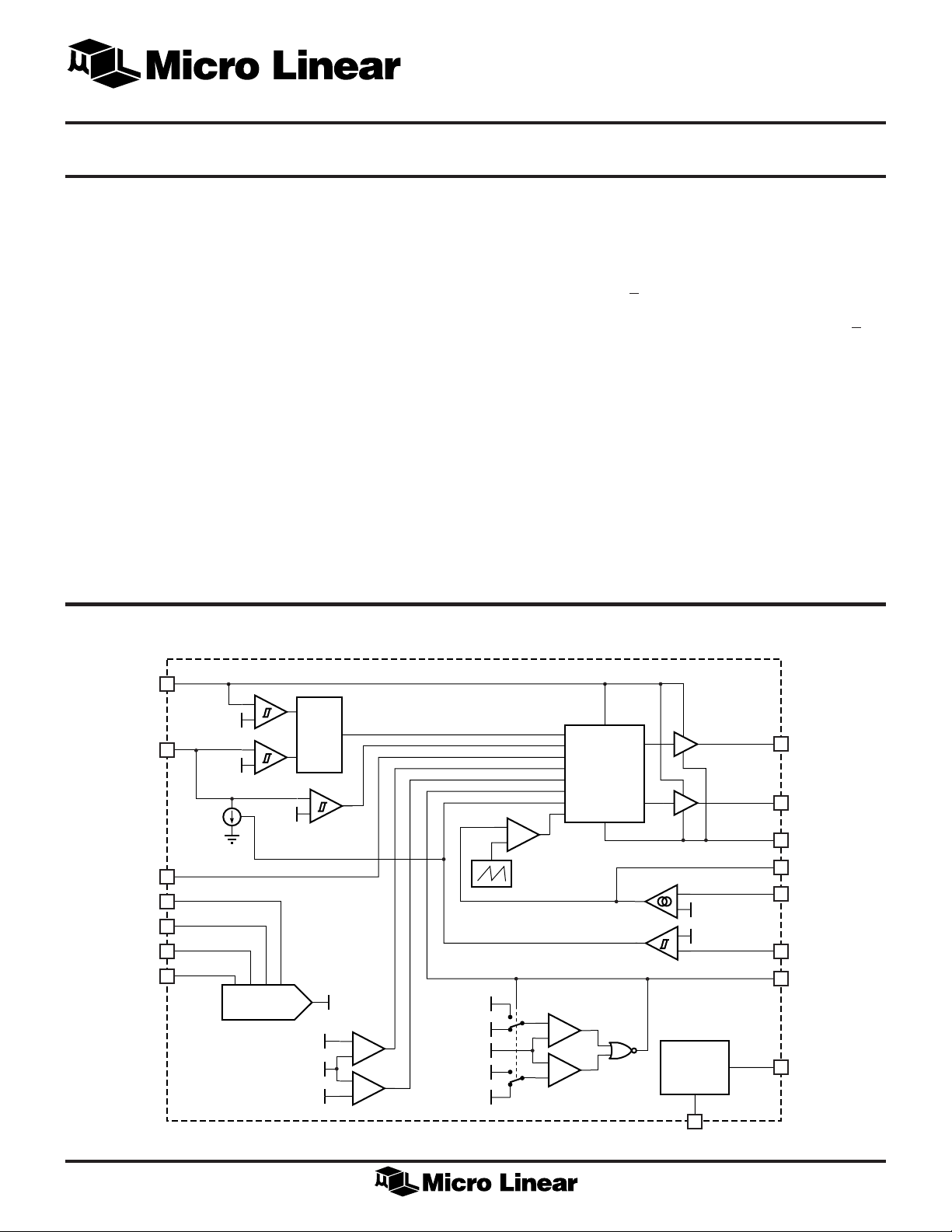
BLOCK DIAGRAM
(Pin Configuration Shown for 16-Pin SOIC Version)
FEATURES
■ Designed to meet Pentium
requirements
■ DC regulation to +1% maximum
■ Proprietary circuitry provides transient response of +5%
maximum over 300mA to 14A load range
■ Programmable output voltage (2.1V to 3.5V) is set by
an onboard 4-bit DAC
■ Synchronous N-channel buck topology for maximum
power conversion efficiency
■ Fixed frequency operation for easier system integration
■ Integrated antishoot-through logic, short circuit
protection, and UV lockout
■ Shutdown control provides load isolation
(* Indicates Part is End of Life as of July 1, 2000)
®
Pro power supply
V
DD
15
PROTECT
16
SHDN
5
D0
1
D1
2
D2
3
D3
4
10.5V
35µA
4.4V
+
–
+
–
4 BIT DAC
V
DAC
V
DAC
4V
UVLO
+ 3%
V
- 3%
N DRV H
CONTROL
LOGIC
+
–
V
DAC
+
–
FB
+
–
V
V
DAC
V
DAC
DAC
V
DAC
+ 10%
+ 3%
- 10%
- 3%
+
–
200kHz
+
V
FB
–
+
–
REFERENCE
+
–
+
–
3.5V
PWR GND
V
DAC
-73mV
PWR GOOD
GND
8
N DRV L
COMP
V
I
SENSE
V
REF
14
13
12
11
FB
9
10
6
7
1
Page 2
ML4900
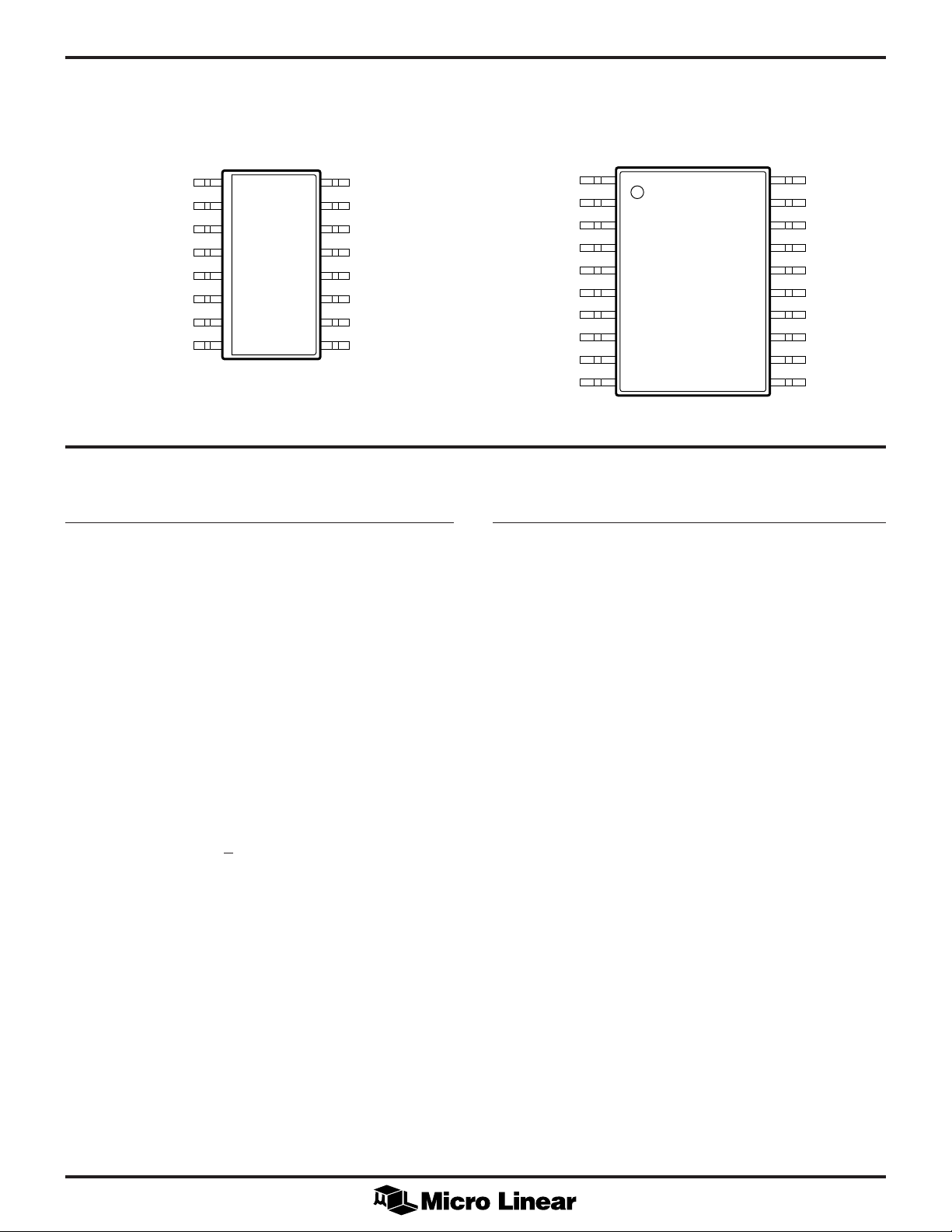
PIN CONFIGURATION
ML4900
16-Pin Narrow SOIC (S16N)
D0
D1
D2
D3
SHDN
PWR GOOD
V
REF
GND
PIN DESCRIPTION
1
2
3
4
5
6
7
8
TOP VIEW
(Pin Number in Parentheses is for TSSOP Version)
PIN NAME FUNCTION
16
15
14
13
12
11
10
PROTECT
V
DD
N DRV H
N DRV L
PWR GND
COMP
ISENSE
9
V
FB
1 (1) D0 LSB input to the DAC which sets
the output voltage
2 (2) D1 Input to the DAC which sets the
output voltage
ML4900
20-Pin TSSOP (T20)
D0
D1
D2
D3
NC
SHDN
NC
PWR GOOD
V
REF
GND
1
2
3
4
5
6
7
8
9
10
TOP VIEW
PIN NAME FUNCTION
20
19
18
17
16
15
14
13
12
11
8 (10) GND Analog signal ground
9 (11) V
10 (12) I
FB
SENSE
Output voltage feedback pin
Current sense input
PROTECT
V
DD
NC
N DRV H
N DRV L
PWR GND
NC
COMP
I
SENSE
V
FB
3 (3) D2 Input to the DAC which sets the
output voltage
4 (4) D3 MSB input to the DAC which sets
the output voltage
5 (6) SHDN Grounding this pin shuts down the
regulator
6 (8) PWR GOOD This open collector output goes
low whenever SHDN goes low or
when the output is not within
+10% of its nominal value
7 (9) V
REF
Bypass connection for the internal
3.5V reference
11 (13) COMP Connection for the compensation
and optional soft-start delay
network
12 (15) PWR GND Power ground
13 (16) N DRV L Synchronous rectifier driver output
14 (17) N DRV H Buck switch driver output
15 (19) V
DD
12V power supply input
16 (20) PROTECT Connection for the integrating
current limit network and the
UVLO monitor for the 5V supply
2
Page 3
ABSOLUTE MAXIMUM RATINGS
ML4900
Absolute maximum ratings are those values beyond which
the device could be permanently damaged. Absolute
maximum ratings are stress ratings only and functional
device operation is not implied.
V
.......................................................................................... 13.5V
DD
Lead Temperature (Soldering, 10 sec) ......................260ºC
Thermal Resistance (qJA)
16-Pin Narrow SOIC ...................................... 100ºC/W
20-Pin TSSOP ................................................. 143ºC/W
Peak Driver Output Current .......................................±2A
VFB Voltage....................................... GND - 0.3V to 5.5V
I
Voltage ................................... GND - 0.5V to 5.5V
SENSE
All Other Analog Inputs ..........GND - 0.3V to VDD + 0.3V
SHDN Input Current .............................................. 100mA
Junction Temperature .............................................. 150ºC
OPERATING CONDITIONS
Temperature Range........................................ 0ºC to 70ºC
VDD Range ...............................................11.4V to 12.6V
PROTECT (5V Supply) Range .................... 4.75V to 5.25V
Storage Temperature Range ...................... –65ºC to 150ºC
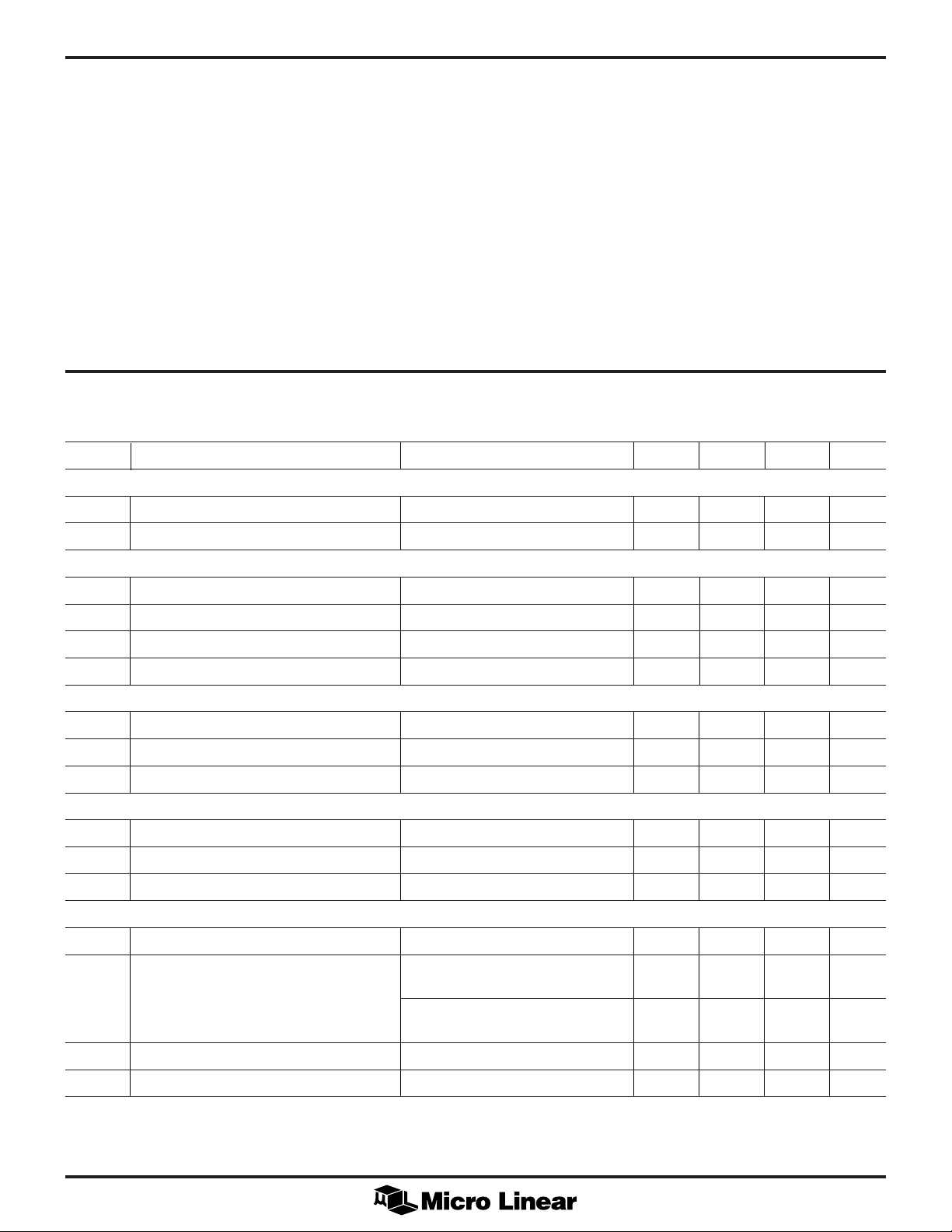
ELECTRICAL CHARACTERISTICS
Unless otherwise specified, VDD = 12V, PROTECT = SHDN = 5V, TA = Operating Temperature Range (Note 1)
SYMBOL PARAMETER CONDITIONS MIN TYP MAX UNITS
REFERENCE
V
UV LOCKOUT
Output Voltage 3.51 3.535 3.56 V
REF
Line Regulation 11V < VDD < 13V 0.5 mV/V
VDD Start-up Threshold 10.2 10.5 10.8 V
VDD Hysteresis 300 450 600 mV
PROTECT (5V) Start-up Threshold 4.25 4.4 4.5 V
PROTECT (5V) Hysteresis 400 450 500 mV
SHUTDOWN
Input Low Voltage 0.8 V
Input High Voltage 2.0 V
Delay to Output 50 ns
POWER GOOD COMPARATOR
Output Voltage in Regulation 5kW pull-up to 5V 4.8 V
Output Voltage out of Regulation VFB < 90% V
Output Voltage in Shutdown SHDN = 0V, 5kW pull-up to 5V 0.4 V
BUCK REGULATOR
Oscillator Frequency 160 200 230 kHz
Duty Cycle Ratio DAC (D3-D0) Code = 0100, 85 95 %
or >110% V
DAC
VFB = 0V
DAC (D3-D0) Code = 0100, 0 %
VFB > 3.193V
DAC
0.4 V
DAC (D3-D0) Input Low Voltage 0.8 V
DAC (D3-D0) Input High Voltage 2.0 V
3
Page 4

ML4900
ELECTRICAL CHARACTERISTICS
SYMBOL PARAMETER CONDITIONS MIN TYP MAX UNITS
BUCK REGULATOR (continued)
VFB Threshold Voltage DAC (D3-D0) Code = 0000 3.495 3.535 3.575 V
(Continued)
DAC (D3-D0) Code = 0001 3.400 3.434 3.468 V
DAC (D3-D0) Code = 0010 3.300 3.333 3.366 V
DAC (D3-D0) Code = 0011 3.200 3.232 3.264 V
DAC (D3-D0) Code = 0100 3.100 3.131 3.162 V
DAC (D3-D0) Code = 0101 3.000 3.03 3.060 V
DAC (D3-D0) Code = 0110 2.900 2.929 2.958 V
DAC (D3-D0) Code = 0111 2.800 2.828 2.856 V
DAC (D3-D0) Code = 1000 2.700 2.727 2.754 V
DAC (D3-D0) Code = 1001 2.600 2.626 2.652 V
DAC (D3-D0) Code = 1010 2.500 2.525 2.550 V
DAC (D3-D0) Code = 1011 2.400 2.424 2.448 V
DAC (D3-D0) Code = 1100 2.299 2.323 2.347 V
DAC (D3-D0) Code = 1101 2.198 2.222 2.246 V
SUPPLY
Note 1:
DAC (D3-D0) Code = 1110 2.097 2.121 2.145 V
DAC (D3-D0) Code = 1111 0.8 V
I
Threshold Voltage -66 -73 -80 mV
SENSE
I
Hysteresis 3mV
SENSE
PROTECT Discharge Current V(I
PROTECT Leakage Current +100 nA
Transition Time, N DRV H and N DRV L CL = 5000pF, 10-90% 40 ns
VDD Current SHDN = 0V 300 450 µA
DAC (D3-D0) Code = 0000
SHDN = 5V, VFB = 5V 1 2 mA
SHDN = 5V, VFB = 0V, CL = 5000pF 30 mA
Limits are guaranteed by 100% testing, sampling, or correlation with worst case test conditions.
) = -100mV 35 mA
SENSE
4
Page 5

FUNCTIONAL DESCRIPTION
ML4900
The ML4900 PWM controller permits the construction of a
simple yet sophisticated power supply for Intel’s Pentium
Pro microprocessor which meets the guidelines of Intel’s
Application Note AP-523. This can be built either as a
Voltage Regulator Module (VRM) or as dedicated
motherboard circuitry. The ML4900 controls two Nchannel MOSFETs in a synchronous buck regulator circuit,
to convert a 5V input to the voltage required by the
microprocessor. The output voltage can be any set to any
one of 15 output voltages from 2.1V to 3.5V, in steps of
100mV, as selected by an onboard DAC. Other features
which facilitate the design of DC-DC converters for any
type of processor include a trimmed 1% reference, special
transient-response optimization in the feedback paths, a
shutdown input, input and output power good monitors,
and overcurrent protection.
4-BIT DAC
The inputs of the internal 4-bit DAC come from open
collector signals provided by the Pentium Pro. These
signals specify what supply voltage the microprocessor
requires. The output voltage of the buck converter is
compared directly with the DAC voltage to maintain
regulation. D3 is the MSB input and D0 is the LSB input of
the DAC. The output voltage set by the DAC is 1% above
the Pentium Pro's nominal operating voltage to counteract
the effects of connector and PC trace resistance, and of the
instantaneous output voltage droop which occurs when a
transient load is applied. The output of the DAC therefore
ranges from 2.121V to 3.535V in 100mV steps. For code
1111, the N DRV H output is disabled, and the output
voltage is zero.
VOLTAGE FEEDBACK LOOP
The ML4900 contains two control loops to improve the
load transient response. The output voltage is directly
monitored via the VFB pin and compared to the desired
output voltage set by the internal 4-bit DAC. When the
output voltage is within +3% of the DAC voltage, the
proportional control loop (closed by the voltage error
amplifier) keeps the output voltage at the correct value. If
the output falls below the DAC voltage by more than 3%,
one side of the transient loop is activated, forcing the
output of the ML4900 to maximum duty cycle until the
output comes back within the +3% limit. If the output
voltage rises above the DAC voltage by more than 3%, the
other side of the transient loop is activated, and the upper
MOSFET drive is disabled until the output comes back
within the +3% limit. During start-up, the transient loop is
disabled until the output voltage is within -3% of the DAC
voltage.
POWER GOOD (PWR GOOD)
An open drain signal is provided by the ML4900 which
tells the microprocessor when the entire power system is
functioning within the expected limits. PWR GOOD will
be false (low) if either the 5V or 12V supply is not in
regulation, when the SHDN pin is pulled low, or when the
output is not within +10% of the nominal output voltage
selected by the internal DAC.
When PWR GOOD is false, the PWR GOOD voltage
window is held to +3%; when PWR GOOD is true (high),
the window is expanded to +10%. Using different
windows for coming into and going out of regulation
makes sure that PWR GOOD does not oscillate during the
start-up of the microprocessor.
INTERNAL REFERENCE
The ML4900 contains a 3.535V, temperature
compensated, precision band-gap reference. The V
is connected to the output of this reference, and should be
bypassed with a 100nF to 220nF ceramic capacitor for
proper operation.
REF
pin
OVERCURRENT PROTECTION
When the output of the buck converter sees an overcurrent
condition (I
the ML4900 will operate in a “hiccup” mode until the
overcurrent condition has been removed.
During an overcurrent condition, a current sink within the
ML4900 draws a small current (35µA) out of the PROTECT
pin for the time during which I
sink is activated over a number of cycles, the voltage on
the PROTECT pin will drop below 4V, signalling a
sustained overcurrent or short circuit at the load. This will
cause the N DRV H output to turn off. The converter will
remain in an off state until the capacitor attached to the
PROTECT pin has charged back to 4.4V, at which time the
converter is re-enabled and tries to resume normal
operation. If the fault causing the overcurrent condition
has not been cleared, the overcurrent protection cycle will
repeat.
exceeds the current limit set point I
OUT
> I
OUT
. If this current
SET
SET
),
UNDERVOLTAGE LOCKOUT
The ML4900 has undervoltage lockout protection circuits
for both the 12V (VDD) and 5V (PROTECT) supplies. The
hysteresis voltage is typically 400mV for each supply.
During an input undervoltage condition, the internal
reference and voltage monitor circuits remain in
operation, but N DRV H and N DRV L are disabled and
the PWR GOOD output will be false (low).
COMPENSATION/SOFT-START
This pin connects to the output of the transconductance
amplifier which forms the gain block for the ML4900’s
proportional control loop. An RC network from this pin to
GND is used to compensate the amplifier.
5
Page 6

ML4900
DESIGN CONSIDERATIONS
This section is a quick-check guide for getting ML4900
circuits up and running, with a special emphasis on
Pentium Pro applications. All component designators refer
to the circuit shown in Figure 1.
COMPENSATION
The R and C values connected to the COMP pin for loop
compensation are 330kW and 33pF, respectively. These
values yield stable operation and rapid transient response
for a most values of L and C
10,000µF), and will generally not need to be altered. If
changes do need to be made, note that the drive capability
of the transconductance error amplifier is typically 10µA,
its Z
approximately 10 MHz.
is 10 MW, and its unity-gain frequency is
OUT
(1µH to 5µH, 1200µF to
OUT
INPUT AND OUTPUT CAPACITORS
The input and output capacitors used in conjunction with
the ML4900, especially in Pentium Pro VRM applications,
must be able to meet several criteria:
1. The input capacitors must be able to handle a relatively
high ripple current
2. The output capacitors must have a low Equivalent Series
Resistance (ESR) and Equivalent Series Inductance (ESL)
3. The output capacitors must be able to hold up the
output during the time that the current through the buck
inductor is slewing to meet a transient load step.
The circuit’s input bypass capacitance should be able to
handle a ripple current equal to 0.5 x I
converter sees load peaks only occasionally, and for less
than 30 seconds at a time during those intervals, then
aluminum electrolytic or OS-Con input capacitors need
only be sized to accommodate the average output load.
Note that tantalum input capacitors have much less
thermal mass than aluminum electrolytics, so this
relaxation of ripple current requirements may not apply to
them.
During a 30A/µs load transient, it is not possible for a buck
converter to slew the output current fast enough to
regulate the voltage in this application. During this
interval, the output capacitance of the converter must act
as passive energy storage. In delivering its energy to the
load, the output capacitance must not introduce any
considerable impedance, or its purpose will be defeated. A
total voltage aberration during load transients of ±5% is
allowed (see Intel AP-523). The voltage transient due to
ESL and ESR is:
For example, assume that a 3.3V output has 3% of the
output's DV contributed by ESR (100mV)and 2% by the
ESL (66mV). To meet this requirement, the output ESR
LOAD
. If the
(1)
should not exceed:
mV
ESR MAX)
With the effects of ESL limited to 2% of 3.3V, the
maximum ESL is:
Achieving these low a values of ESL and ESR is not trivial;
doing so typically requires using several high-quality
capacitors in parallel.
The output capacitance should have a value of > 2200µF
to hold the output voltage relatively constant (< 50mV of
sag) until the current in the buck inductor can catch up
with the change in output current. To meet the ESR and
ESL requirements, the actual output capacitance will
usually be significantly greater than this theoretical
minimum. These capacitors can be of all one type, or a
combination of aluminum electrolytic, OS-Con, and
tantalum devices.
100
==
137
.
73
Am(.
W
(2)
(3)
OVERCURRENT PROTECTION
Current sense resistor R1 is used to monitor the inductor
current during the off period, i.e., while current is flowing
through the synchronous rectifier (or Schottky diode, if no
synchronous rectifier MOSFET is used). The internal
current sense comparator has been designed to provide in
excess of 14A of output current when used with a 5mW
resistor. R1 must be a low inductance part such as Dale/
Vishay’s type WSL-2512-.005±2.5%. This is a 5mW surface
mount part rated at 1 Watt. Using a PCB trace as a current
sense element is not recommended due to the high
temperature coefficient of copper, and due to etching and
plating tolerances which can occur from board to board.
The R and C values connected to the PROTECT pin for
setting the current limit delay and the off-time of the
hiccup mode are 100kW and 1µF, respectively. These
values will protect most MOSFETs from overheating
during a short circuit condition. If it is necessary to change
the ratio of ON and OFF times during overcurrent
conditions, this can be done by selecting a different value
for C13. Larger values of C13 will increase the delay
between retry attempts (the length of the “hiccup”).
The voltage across current sense resistor R1 must be
Kelvin-sensed. This ensures that the ML4900 monitors only
the voltage across this resistor and not the voltage drops or
inductive transients in the PCB traces which carry current
into and out of this resistor. The two pins of the ML4900
which must be Kelvin-connected to the sense resistor are
I
and GND. There is no connection inside the
SENSE
ML4900 between GND (pin 8) and PWR GND (pin 12).
This is to facilitate the requisite Kelvin-sensing of the
voltage across R1. Because of this, there must be a good
electrical connection between the ML4900 PWR GND
6
Page 7

5V
IN
12V
OUTEN
UP#
VID0
VID1
VID2
VID3
PWRGD
C8
220nF
16V
ML4900
IN
D1
BAW56
C11
22µF
25V
1
D0
2
D1
3
D2
4
D3
5
SHDN
6
PWR GOOD
7
V
REF
8
GND
C10
220nF
16V
ML4900
PWR GND
PROTECT
V
DD
N DRV H
N DRV L
COMP
I
SENSE
V
FB
16
15
14
13
12
11
10
9
R3
330kΩ
C9
33pF
C13
1µF
16V
R5
100kΩ
1kΩ
C12
220nF
16V
R4
5m
Q1
Q2
R1
1W
3X
1800µF
10V
L2
1.4µH
C3C1 C2
VCCP
4X
C4 C5 C6 C7
1800µF
10V
V
Ω
SS
Figure 1. Pentium Pro VRM Circuit
and GND pins. At the same time, PWR GND must have a
low impedance connection to the ground plane used on
the board, as high instantaneous currents will flow in PWR
GND when N DRV L and N DRV H switch the capacitive
loads of the output MOSFET gates. A layout technique
which satisfies these requirements is to return PWR GND
to the grounded end of R1 using a high current Kelvin
connection. Figure 2 shows one successful
implementation of these PCB layout requirements.
I
is an input to a medium-speed, high-sensitivity
SENSE
comparator. It is often helpful to shield the trace running
from R1 to I
with a “guard trace” connected to circuit
SENSE
ground.
The compensation components R3 and C9 are highimpedance nodes connected to the output of the voltage
loop error amplifier. These components should be kept in
close proximity to the ML4900. C9 should be returned to
GND, not to PWR GND or the ground plane of the PC
board. It may be helpful to shield the trace running from
R3 to COMP with a “guard trace” connected to circuit
ground.
Keep the V
bypass capacitor C8 close to the ML4900.
REF
Ensure that its ground connection is to GND, not PWR
GND or the ground plane of the PCB.
The VDD bypass capacitors C10 and C11 should be
returned to PWR GND or to the PC board ground plane.
They should not be returned to GND due to high transient
currents which could interfere with the current sensing
function.
In order to reduce circuit size, complexity, and cost, direct
drive of all N-channel power MOSFETs in the output stage
is employed, derived from the 12V input bus. This delivers
at least 10V of VGS enhancement to the MOSFET(s)
performing the synchronous rectification function. The
power switching MOSFET(s), however, have a worst-case
VGS enhancement of about 6V, and must therefore be
logic-level parts.
If a given design uses power MOSFETs in an 8 pin SOIC
package style, keep in mind that the thermal dissipation
capability of these parts is largely dictated by the copper
area available to their drains. A good layout will maximize
this area.
TO
SYNCHRONOUS
RECTIFIER
MOSFET
SOURCE
SENSE
RESISTOR
POWER GROUND RETURN
(GROUND PLANE)
I
SENSE
TO
PWR GND
GND
TO
TO
Figure 2. Kelvin Sense Connections
7
Page 8

ML4900
PHYSICAL DIMENSIONS
16
0.017 - 0.027
(0.43 - 0.69)
(4 PLACES)
0.055 - 0.061
(1.40 - 1.55)
1
0.251 - 0.262
(6.38 - 6.65)
20
inches (millimeters)
Package: S16N
16-Pin Narrow SOIC
0.386 - 0.396
(9.80 - 10.06)
PIN 1 ID
0.050 BSC
(1.27 BSC)
0.012 - 0.020
(0.30 - 0.51)
0.059 - 0.069
(1.49 - 1.75)
SEATING PLANE
Package: T20
20-Pin TSSOP
0.148 - 0.158
(3.76 - 4.01)
0.004 - 0.010
(0.10 - 0.26)
0.228 - 0.244
(5.79 - 6.20)
0º - 8º
0.015 - 0.035
(0.38 - 0.89)
0.006 - 0.010
(0.15 - 0.26)
0.033 - 0.037
(0.84 - 0.94)
1
0.008 - 0.012
PIN 1 ID
(0.20 - 0.30)
0.026 BSC
(0.65 BSC)
0.169 - 0.177
(4.29 - 4.50)
0.043 MAX
(1.10 MAX)
SEATING PLANE
0.246 - 0.258
(6.25 - 6.55)
0.002 - 0.006
(0.05 - 0.15)
0º - 8º
0.020 - 0.028
(0.51 - 0.71)
0.004 - 0.008
(0.10 - 0.20)
ORDERING INFORMATION
PART NUMBER TEMPERATURE RANGE PACKAGE
ML4900CS (End Of Life) 0ºC to 70ºC 16-Pin Narrow SOIC (S16N)
ML4900CT (Obsolete) 0ºC to 70ºC 20-Pin TSSOP (T20)
© Micro Linear 1997 is a registered trademark of Micro Linear Corporation. Pentium is a registered trademark of Intel Corporation.
Products described herein may be covered by one or more of the following patents: 4,897,611; 4,964,026; 5,027,116; 5,281,862; 5,283,483; 5,418,502; 5,508,570; 5,510,727; 5,523,940; 5,546,017;
5,559,470; 5,565,761; 5,594,376. Other patents are pending.
Micro Linear reserves the right to make changes to any product herein to improve reliability, function or design.
Micro Linear does not assume any liability arising out of the application or use of any product described herein,
neither does it convey any license under its patent right nor the rights of others. The circuits contained in this
data sheet are offered as possible applications only. Micro Linear makes no warranties or representations as to
whether the illustrated circuits infringe any intellectual property rights of others, and will accept no
responsibility or liability for use of any application herein. The customer is urged to consult with appropriate
legal counsel before deciding on a particular application.
8
2092 Concourse Drive
San Jose, CA 95131
Tel: 408/433-5200
Fax: 408/432-0295
DS4900-01
 Loading...