

Page 1
July 2000
ML4866*
3.3V Output DC–DC Step-Down Converter
GENERAL DESCRIPTION
The ML4866 is a high efficiency pulse width modulated
(PWM) buck regulator designed for use in 5V systems or
portable equipment that need a compact, efficienct 3.3V
supply. It has a switching frequency of 120kHz and uses
synchronous rectification to optimize power conversion
efficiency. Unlike other solutions, the ML4866 requires no
external diodes or FETs.
The ML4866 can provide up to 500mA of output current,
and operates over an input voltage range of 3.5V to 6.5V
(3 to 4 cells or a 5 VDC supply). A complete switched
mode power converter can be quickly and easily
implemented with few external components. Thanks to a
built-in autoburst mode, power conversion efficiency of
this DC–DC converter can exceed 90% over more than 2
decades of output load current.
Stability and fast loop response are provided by current
programming and a current sense circuit. The ML4866
also has a SHDN pin for use in systems which have power
management control. Undervoltage lockout and soft start
are also built in.
FEATURES
■ High power conversion efficiency over 2 decades of
load current
■ No external FETs or diodes; minimum external
components
■ 3.5V to 6.5V input voltage range
■ Significantly extends battery life over linear regulator
based solutions
■ Micropower operation
■ Low shutdown mode quiescent current
(* Indicates Part is End Of Life as of July 1, 2000)
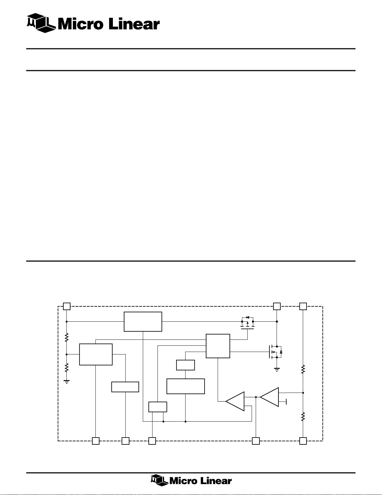
BLOCK DIAGRAM
5
V
IN
UVLO/
SHUTDOWN
6
SHDN
REFERENCE
V
3
CURRENT
SENSE
REF
BURST
BURST
4
OSC
SLOPE
COMPENSATION
BUCK
CONTROL
–
+
ERROR
AMPLIFIER
COMP
2
7
V
–
+
1
V
L
V
REF
OUT
GND
8
1
Page 2
ML4866
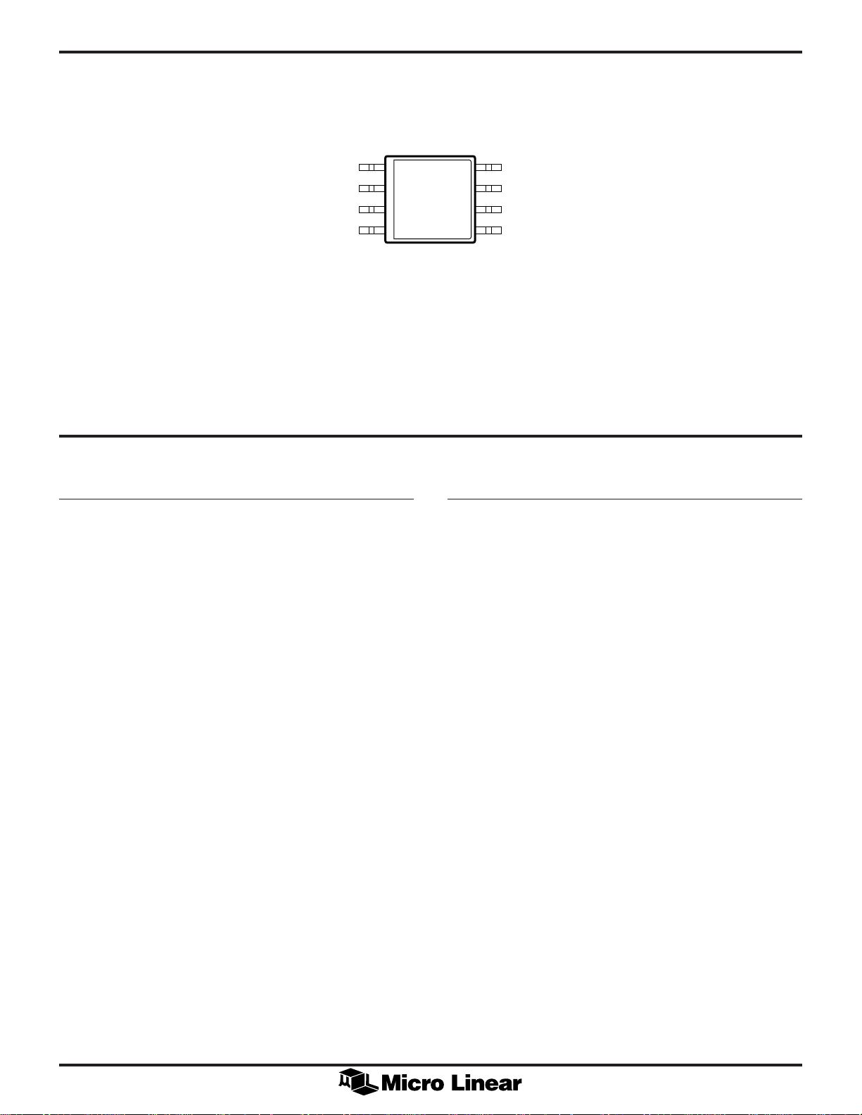
PIN CONFIGURATION
ML4866
8-Pin SOIC (S08)
V
OUT
COMP
V
REF
BURST
PIN DESCRIPTION
PIN NAME FUNCTION
1V
OUT
2 COMP Connection point for an external
Regulated 3.3V output
compensation network
1
2
3
4
TOP VIEW
8
7
6
5
PIN NAME FUNCTION
5V
IN
GND
V
L
SHDN
V
IN
Input voltage
6 SHDN Pulling this pin low shuts down the
regulator
3V
REF
1.25V reference output
4 BURST This pin controls when the control
circuit switches between PWM and
PFM modes of operation
7V
L
Buck inductor connection
8 GND Ground
2
Page 3

ML4866
ABSOLUTE MAXIMUM RATINGS
Absolute maximum ratings are those values beyond which
the device could be permanently damaged. Absolute
maximum ratings are stress ratings only and functional
device operation is not implied.
OPERATING CONDITIONS
Temperature Range
ML4866CS ................................................. 0ºC to 70ºC
ML4866ES .............................................. -20ºC to 70ºC
ML4866IS ............................................... -40ºC to 85ºC
VIN Operating Range ...................................3.5V to 6.5V
V
................................................................................................... 7V
IN
Voltage on any other pin .........GND - 0.3V to VIN + 0.3V
Peak Switch Current (I
Average Switch Current (I
) ......................................... 2A
PEAK
).....................................1A
AVG
Junction Temperature.............................................. 150ºC
Storage Temperature Range ....................... -65ºC to 150ºC
Lead Temperature (Soldering 10 Sec.)..................... 260ºC
Thermal Resistance (qJA).................................... 160ºC/W
ELECTRICAL CHARACTERISTICS
Unless otherwise specified, VIN = 5V, L = 50µH, C
TA = Operating Temperature Range (Note 1)
SYMBOL PARAMETER CONDITIONS MIN TYP MAX UNITS
REFERENCE
V
REF
PWM REGULATOR
Output Voltage 0 < I(V
= 100µF, R
OUT
) < –5µA, I
REF
COMP
OUT
= 390kW, C
= 0mA 1.22 1.25 1.27 V
COMP
= 15nF,
f
OSC
SHUTDOWN
Oscillator Initial Accuracy I
Oscillator Total Variation Line and Temp 90 130 185 kHz
Soft Start VIN to V
BURST Burst Mode Threshold 250 400 mV
BURST PWM Mode Threshold 500 850 mV
BURST Bias Current 35 µA
Output Voltage I
Line Regulation VIN = 4V to 6.5V, TA = 25°C ±2 %
Load Regulation I
Temperature Stability TA = -40°C to 85°C ±1 %
Total Variation Line, Load, Temp ±5 %
UVLO Startup Threshold 3.2 3.5 V
UVLO Shutdown Threshold 2.9 3.1 V
Delay 3 5 ms
OUT
= 200mA, TA = 25°C 100 115 165 kHz
OUT
= 200mA 3.2 3.3 3.4 V
OUT
I
= 20mA, BURST = 0V 3.28 3.38 3.48 V
OUT
= 100mA to 500mA, ±2.5 %
OUT
TA = 25°C
I
= 5mA to 100mA, ±2.5 %
OUT
BURST = 0V, TA = 25°C
SHDN Threshold 2V
SHDN Bias Current –5 µA
3
Page 4

ML4866
ELECTRICAL CHARACTERISTICS
SYMBOL PARAMETER CONDITIONS MIN TYP MAX UNITS
SUPPLY
I
Note 1: Limits are guaranteed by 100% testing, sampling, or correlation with worst case test conditions.
VIN Current I
IN
(Continued)
= 0mA, BURST = 5V 400 500 µA
OUT
I
= 0mA, BURST = 0V 120 220 µA
OUT
SHDN = 0V 20 35 µA
FUNCTIONAL DESCRIPTION
The ML4866 is a current-mode, step-down (buck)
converter designed to keep the buck inductor current in
the continuous conduction mode (CCM). Current-mode
operation provides faster output response to input voltage
and output current changes along with cycle-by-cycle
current limiting. CCM inductor current is preferred when
the highest conversion efficiencies are required.
For high efficiencies at low output current, the ML4866
contains an autoburst function which automatically
switches from pulse width modulation (PWM) to pulsed
frequency modulation (PFM) operation when the output
current drops below 100mA. Selection of either mode is
possible by applying the correct logic level signal to the
BURST pin. When operating in PWM mode, loop
compensation of the ML4866 is simplified due to its
transconductance type error amplifier.
An under voltage lockout (UVLO) circuit within the
ML4866 enables the converter when the input voltage
is greater than 3.25V and disables it when the input
voltage is below 3.10V. The IC can also be disabled
externally by applying a logic low signal to the SHDN
pin. When disabled, the ML4866 draws less than 20µA of
current.
ramping the inductor current down to 0mA. This action is
repeated until the output voltage returns to its nominal
setting and begins again when the output drops below its
nominal setting. The rate or frequency at which this
“bursting” occurs is directly proportional to the output
current. When the average output current rises above
130mA, the ML4866 returns to PWM operation.
For applications having a load current range of less than
100mA and greater than 130mA, the BURST pin should be
left open and bypassed to ground with a 15nF or larger
capacitor. It is possible to tailor an application for the
highest possible efficiency by externally forcing the
ML4866 into either control mode. Applying a logic low
level to BURST forces the IC into PFM mode. Conversely,
a logic high places it in PWM mode. Care should be
taken to avoid reducing the efficiency by placing the
controller in the least efficient mode for a given output
current.
The internal 1.25V bandgap reference is made available
via the V
pin, and may be used for general
REF
applications requiring less than 10µA of current. For
proper operation, this pin must always be bypassed to
GND with a 100nF capacitor.
BURST MODE
Burst (PFM) mode is a method of regulating the output
voltage by applying a variable frequency modulation
technique to the buck inductor. This method maintains
higher efficiencies at light loads than if PWM were used.
If BURST is left open, the ML4866 switches from PWM
mode to PFM mode when the output current falls below
100mA. When the output voltage falls out of regulation
while in PFM mode, the internal buck switch turns on and
ramps the inductor current up to 300mA. The buck switch
then turns off and the synchronous switch turns on,
4
V
– V
IN
OUT
L
Figure 1. Inductor Current
–V
OUT
L
∆I
Page 5

ML4866
DESIGN CONSIDERATIONS
INDUCTOR SELECTION
Figure 1 shows the inductor current in a step-down
converter operating in CCM. Note that the inductor
current does not reach zero during each switching cycle.
This is unlike discontinuous conduction mode (DCM)
where the inductor current is allowed to reach zero. CCM
operation generally results in lower peak to peak output
ripple voltage and higher circuit efficiencies because of
lower peak and RMS currents in the switching FETs and
buck inductor. The minimum value of inductance required
for CCM operation with a 6.5V input and a load range of
100mA to 500mA is:
VV V
-
()
L
L
OUT IN MAX OUT
>
VI f
2
IN MAX OUT MIN SW
() ()
33 65 33
.(. .)
VmAkHz
2 65 100 120
.
To guarantee reliable operation, the peak inductor current
must be between 80% and 85% of its maximum rated
value. This value is the sum of the inductor peak to peak
current and the maximum output current:
-
I
LP P
I
LP P()
II
LPEAK OUT MAX
II
L PEAK OUT MAX() ()
2
=
()
–
-
2 3 465 40 3465
=
–
=+
() ()
=+
For the highest efficiency, inductor core and copper losses
must be minimized. Good high frequency core material
such as Kool-Mu, ferrite or Molyperm are popular choices
for this converter. Disregarding physical size
requirements, the lowest loss inductor will generally be
the one with the highest peak current rating.
Figure 2 displays the efficiency of the ML4866 under
various input voltage and output current conditions. These
results were obtained using a Coiltronics CTX100-4
inductor having the following specifications:
()
VVV
-
VVV
OUT MAX IN MIN OUT MAX
() () ()
Vf L
.(..)
VV V
.
VkHz H
m
40 90 100
()
IN MIN SW MIN
VVV
() ()
-
OUT MAX IN MIN OUT MAX
.(..)
3465 40 3465
.
40 120 100
()
() () ()
VfL
IN MIN SW
()
-
VV V
m
VkHz H
H>
>
68
m
=
103
mA
=
550
(1)
(2)
(3)
mA
100
98
96
94
I
= 10mA
OUT
92
EFFICIENCY (%)
90
88
I
= 500mA
OUT
86
4.0 5.0 6.55.5
3.5 4.5 6.0
I
= 100mA
OUT
INPUT VOLTAGE (V)
Figure 2. Efficiency vs. Input Voltage
A partial listing of inductor manufacturers with standard
parts which meet the criteria for use with the ML4866 is
given below.
Coiltronics (561) 241-7876
Dale (605) 665-9301
Coilcraft (847) 639-6400
XFMRS, Inc (317) 834-1066
Sumida (847) 956-0666
CAPACITOR SELECTION
A typical digital system requires a peak to peak output
ripple voltage of no greater than 1% to 3% of the nominal
output voltage. In a step-down converter, the largest
contributor to ripple voltage is almost always the product
of the inductor peak-to-peak current times the output
capacitor’s equivalent series resistance. To select the
correct capacitor, first calculate the minimum
capacitance value required:
VV V
-
()
C
>
OUT
C
>
OUT
OUT IN MAX OUT
VVLf
8
P P MAX IN MAX SW
-
() ()
mV V H kHz
m
8 33 65 100 120
()
.(. .)
33 65 33
VV
-
.
2
2
(4)
m
.
>
427
Next, calculate the maximum permissible ESR of the
output capacitor:
F
Nominal Inductance - 100µH
Peak Current Rating - 950mA
DC Resistance - 175mW
(. )
0033
ESR <<
(.)
01
.
033
W
(5)
When limited space is available, tantalum capacitors are
the best choice. Electrolytic capacitors can be used and
will be less expensive, but the ESR for low capacitance
values as needed here will be much higher than for the
same value tantalum. Table 2 lists the ESR values for a
number of general purpose tantalum capacitors which are
widely available from a number of sources. A 47µF
capacitor was chosen for the design example.
5
Page 6

ML4866
DESIGN CONSIDERATIONS
(Continued)
FREQUENCY COMPENSATION
Frequency compensation of the ML4866 is required when
the converter is operating in PWM mode. Two simple
methods are provided to ensure the converter is frequency
stable. Both these methods will work only if the inductor
current is selected to be in CCM at the maximum load
current (see Inductor Selection). The first, called dominant
pole compensation, is used when non-varying loads are
expected. This method requires a single capacitor
connected from the error amplifier output (COMP Pin) to
ground.
For loads which change suddenly, the transient response
(or bandwidth) of the circuit must be increased to prevent
the output voltage from going outside of the regulation
band. The method used to accomplish this is called
zero/pole compensation and requires a series resistor
capacitor network from COMP to ground.
To determine which method works best for a given
application, apply the components found from the
zero/pole compensation method to an actual circuit
and examine the output voltage variation. If the voltage
variation is acceptable, connect the simpler, single
capacitor and re-check the output voltage for acceptable
load transient response.
VARYING LOAD CURRENT
To minimize output voltage variations due to rapidly
changing load currents, use the series RC zero
compensation method to find the compensation network
component values that will improve the output voltage
response to load transients.
The unity gain bandwidth of the converter is extended to
15kHz using an RC network determined by:
R
C
COMP
COMP
G
>=,
g
m
=
50
p
Where f0 = 15kHz, f
390kW, 5%), and C
where G
1
R
COMP
COMP
= 16nF (use 15nF).
COMP
f
O
f
COMP
= 640Hz, R
> 375kW (use
COMP
(7)
(8)
Either method of compensation for CCM mode with result
in continued stability as the ML4866 changes to DCM
mode at lighter load currents. Figure 3 shows a typical
application circuit for the ML4866.
NON-VARYING LOAD CURRENT
For the best possible response to load transients using only
a single capacitor, dominant pole compensation is
implemented with a single capacitor value of:
g
C
COMP
Where f
COMP
gm = 62.5µmho, and C
18nF or 22nF capacitor). The value of C
m
=
f
2
COMP
is the unity gain crossover point (640Hz),
> 15.5nF (choose a standard
COMP
COMP
can be
(6)
increased but at the risk of increased output voltage
variations with transient loads.
VOLTAGE ESR @
CAPACITANCE RATING SIZE 100kHz
4.7µF 16V 3216 0.490W
10µF 6.3V 3216 0.368W
22µF 16V 7343 0.149W
33µF 6.3V 6032 0.291W
47µF 10V 7343 0.144W
100µF 6.3V 7343 0.088W
390kΩ
15nF
100nF
V
OUT
COMP
V
REF
BURST
15nF
100µH
ML4866
1
2
3
4
8
7
6
5
GND
V
SHDN
V
100µF
V
OUT
3.3V
33µF
L
IN
V
3.5V to 6.5V
100nF
IN
Table 2. ESR Values for Low Cost Tantalum Capacitors
6
Figure 3. Typical Application Circuit
Page 7

LAYOUT
For proper performance, all components should be placed
as close to the ML4866 as possible. Particular attention
should be paid to minimize the length of the connections
between the COMP and V
bringing these traces and the associated components
close to VL.
It is always recommended that a 10µF or greater
capacitor be connected to VIN of the ML4866. A 33µF
tantalum capacitor and 100nF film or ceramic capacitor
is recommended when powering the ML4866 from
Lithium or Alkaline cells.
Ground and power planes must be large enough to carry
the current the converter has been designed to supply.
A sample PC board layout is shown in Figure 4.
pins to GND. Also avoid
REF
ML4866
Figure 4. Sample PC Board Layout
7
Page 8

ML4866
PHYSICAL DIMENSIONS
0.017 - 0.027
(0.43 - 0.69)
(4 PLACES)
0.055 - 0.061
(1.40 - 1.55)
inches (millimeters)
Package: S08
8-Pin SOIC
0.189 - 0.199
(4.80 - 5.06)
8
PIN 1 ID
1
0.050 BSC
(1.27 BSC)
0.012 - 0.020
(0.30 - 0.51)
SEATING PLANE
0.148 - 0.158
(3.76 - 4.01)
0.059 - 0.069
(1.49 - 1.75)
0.004 - 0.010
(0.10 - 0.26)
0.228 - 0.244
(5.79 - 6.20)
0º - 8º
0.015 - 0.035
(0.38 - 0.89)
0.006 - 0.010
(0.15 - 0.26)
ORDERING INFORMATION
PART NUMBER TEMPERATURE RANGE PACKAGE
ML4866CS (End Of Life)0ºC to 70ºC8-Pin SOIC (S08)
ML4866ES (EOL) -20ºC to 70ºC8-Pin SOIC (S08)
ML4866IS (Obsolete)-40ºC to 85ºC8-Pin SOIC (S08)
© Micro Linear 1997. is a registered trademark of Micro Linear Corporation. All other trademarks are the property of their respective owners.
Products described herein may be covered by one or more of the following U.S. patents: 4,897,611; 4,964,026; 5,027,116; 5,281,862; 5,283,483; 5,418,502; 5,508,570;
5,510,727; 5,523,940; 5,546,017; 5,559,470; 5,565,761; 5,592,128; 5,594,376; 5,652,479; 5,661,427; 5,663,874. Japan: 2,598,946; 2,619,299. Other patents are pending.
Micro Linear reserves the right to make changes to any product herein to improve reliability, function or design. Micro Linear does not assume any liability arising out of
the application or use of any product described herein, neither does it convey any license under its patent right nor the rights of others. The circuits contained in this data
sheet are offered as possible applications only. Micro Linear makes no warranties or representations as to whether the illustrated circuits infringe any intellectual property
rights of others, and will accept no responsibility or liability for use of any application herein. The customer is urged to consult with appropriate legal counsel before
deciding on a particular application.
8
DS4866-01
2092 Concourse Drive
San Jose, CA 95131
Tel: (408) 433-5200
Fax: (408) 432-0295
www.microlinear.com
9/8/97 Printed in U.S.A.
 Loading...