

Page 1
July 2000
FEATURING
Extended Commercial Temperature Range
-20˚C to 70˚C
for Portable Handheld Equipment
ML4863*
High Efficiency Flyback Controller
GENERAL DESCRIPTION
The ML4863 is a flyback controller designed for use in
multi-cell battery powered systems such as PDAs and
FEATURES
■ Variable frequency current mode control and
synchronous rectification for high efficiency
notebook computers. The flyback topology is ideal for
systems where the battery voltage can be either above or
■ Minimum external components
below the output voltage, and where multiple output
voltages are required.
■ Guaranteed start-up and operation over a wide input
voltage range (3.15V to 15V)
The ML4863 uses the output voltage as the feedback
control signal to the current mode variable frequency
flyback controller. In addition, a synchronous rectifier
■ High frequency operation (>200kHz) minimizes the
size of the magnetics
control output is supplied to provide the highest possible
conversion efficiency (greater than 85% efficiency over a
1mA to 1A load range).
The ML4863 has been designed to operate with a
■ Flyback topology allows multiple outputs in addition to
the regulated 5V
■ Built-in overvoltage and current limit protection
minimum number of external components to optimize
space and cost. *Some Packages Are Obsolete
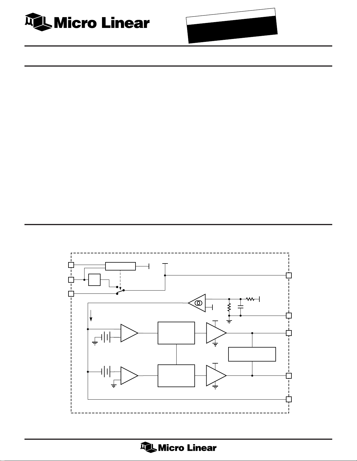
BLOCK DIAGRAM
3
1
4
SHDN
V
IN
V
FB
R
gm
4.5V
LDO
I
BIAS & UVLO
18mV
18mV
CURRENT
COMPARATOR
+
COMP
–
RECTIFIER
COMPARATOR
–
COMP
+
V
FB
V
CC
SWITCHING
CONTROL
BLANKING
V
CC
5
–
+
V
REF
V
CC
A1
CROSS-CONDUCTION
PROTECTION
A2
V
CC
V
FB
GND
8
OUT 1
6
OUT 2
7
SENSE
2
1
Page 2
ML4863
PIN CONFIGURATION
PIN DESCRIPTION
8-Pin SOIC (S08)
V
IN
SENSE
SHDN
V
FB
TOP VIEW
ML4863
1
2
3
4
8
GND
7
OUT 2
6
OUT 1
5
V
CC
PIN NAME FUNCTION
1V
IN
Battery input voltage
2 SENSE Secondary side current sense
3 SHDN Pulling this pin high initiates a
shutdown mode to minimize battery
drain
4V
FB
Feedback input from transformer
secondary, and supply voltage when
V
> 4.5V
OUT
PIN NAME FUNCTION
5V
CC
Internal power supply node for
connection of a bypass capacitor
6 OUT 1 Flyback primary switch MOSFET driver
output
7 OUT 2 Flyback synchronous rectifier MOSFET
driver output
8 GND Analog signal ground
2
Page 3
ABSOLUTE MAXIMUM RATINGS
ML4863
Absolute maximum ratings are those values beyond which
the device could be permanently damaged. Absolute
Lead Temperature (Soldering 10 Sec.) ..................... 260ºC
Thermal Resistance (qJA) .................................... 160ºC/W
maximum ratings are stress ratings only and functional
device operation is not implied.
V
................................................................. GND – 0.3V to 18V
IN
Voltage on any other pin ........................... GND – 0.3V to 7V
Source or Sink Current (OUT1 & OUT2)...................... 1A
Junction Temperature ..............................................150ºC
Storage Temperature Range...................... –65ºC to 150ºC
OPERATING CONDITIONS
Temperature Range
ML4863CS................................................. 0ºC to 70ºC
ML4863ES ............................................. –20ºC to 70ºC
ML4863IS .............................................. –40ºC to 85ºC
VIN Operating Range ...................................3.15V to 15V
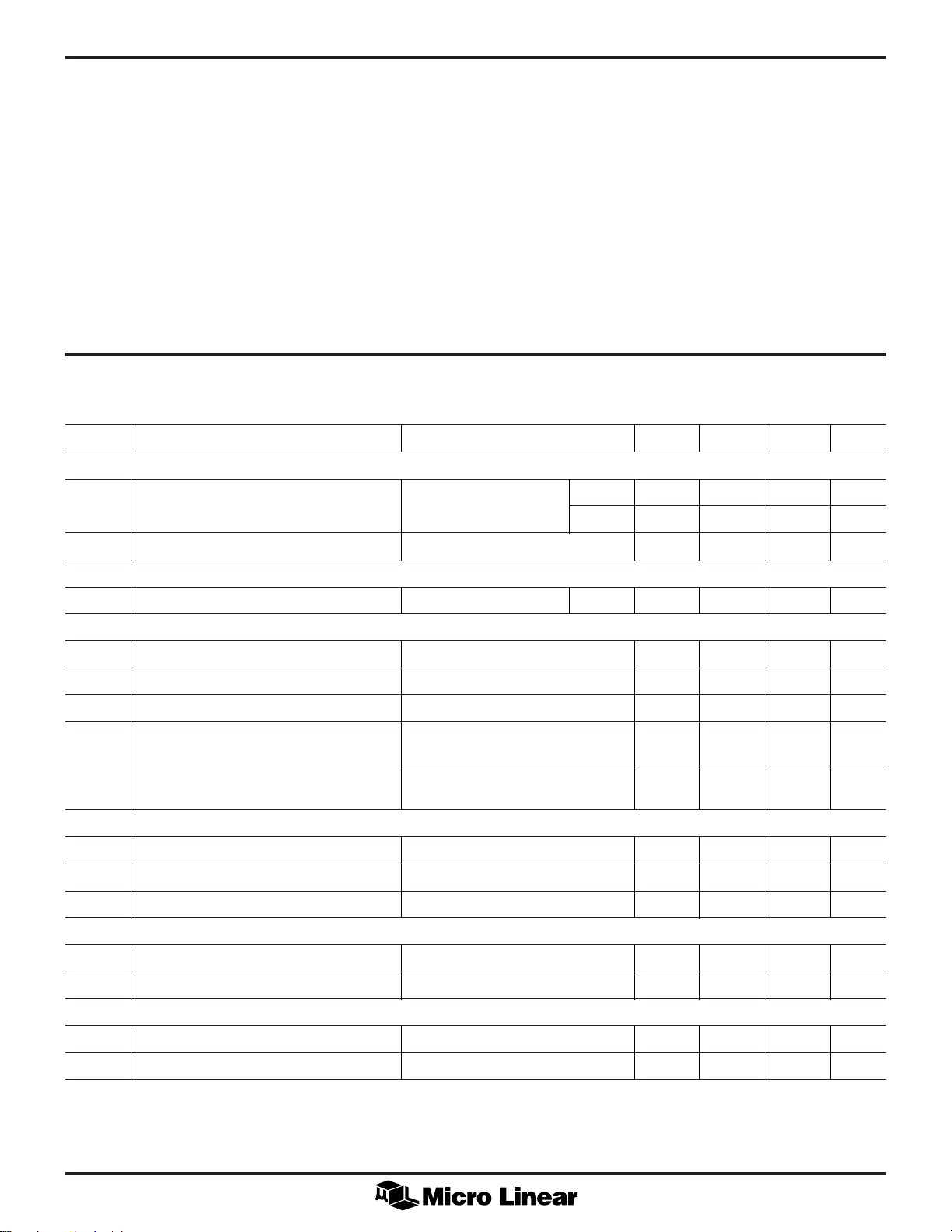
ELECTRICAL CHARACTERISTICS
Unless otherwise specified, VIN = 12V, TA = Operating Temperature Range (Note 1)
SYMBOL PARAMETER CONDITIONS MIN TYP MAX UNITS
OSCILLATOR
t
ON
ON Time C Suffix 2.1 2.5 2.8 µs
E/I Suffix 2.1 2.5 2.95 µs
Minimum Off Time VFB = 0V 450 650 850 ns
VFB REGULATION
Total Variation Line, Load, & Temp 4.85 5 5.15 V
OUTPUT DRIVERS
OUT1 Rise Time C
OUT1 Fall Time C
OUT2 Rise Time C
OUT2 Fall Time Continuous Mode, C
SHDN
Input High Voltage 2.0 V
Input Low Voltage 0.8 V
Input Bias Current SHDN = 5V 5 10 µA
SENSE
SENSE Threshold – Full Load VIN = 5V, VFB = V
SENSE Threshold – Short Circuit VFB = 0V 235 mV
CIRCUIT PROTECTION
= 3nF, 20% to 90% of V
LOAD
= 3nF, 90% to 20% of V
LOAD
= 3nF, 20% to 90% of V
LOAD
90% to 20% of V
Discontinuous Mode, C
90% to 20% of V
LOAD
CC
CC
FB (No Load)
CC
CC
CC
= 3nF,
= 3nF,
LOAD
– 100mV 130 150 160 mV
60 70 ns
60 70 ns
60 70 ns
60 70 ns
125 150 ns
Undervoltage Lockout Start-up Threshold 3.0 3.15 V
Undervoltage Lockout Hysteresis 0.5 0.6 V
3
Page 4

ML4863
ELECTRICAL CHARACTERISTICS
SYMBOL PARAMETER CONDITIONS MIN TYP MAX UNITS
SUPPLY
I
FB
I
V
Note 1: Limits are guaranteed by 100% testing, sampling, or correlation with worst case test conditions.
VFB Quiescent Current 100 150 µA
VIN Shutdown Current SHDN = 5V 20 25 µA
IN
VCC Output Voltage VFB = 0V, VIN = 15V, C
CC
(Continued)
SHDN = 5V, VIN < 6V 5 10 µA
= 0.1µF 4.5 5.5 V
VCC
VFB = 0V, VIN = 6V, C
VFB = 0V, VIN = 3.15V, C
VFB = 5V 4.5 5 5.15 V
= 0.1µF 4.0 5.0 V
VCC
= 0.1µF 2.8 V
VCC
4
Page 5

FUNCTIONAL DESCRIPTION
ML4863
The ML4863 utilizes a flyback topology with constant ontime control. The circuit determines the length of the offtime by waiting for the inductor current to drop to a level
determined by the feedback voltage (VFB). Consequently,
the current programming is somewhat unconventional
because the valley of the current ripple is programmed
instead of the peak. The controller automatically enters
burst mode when the programmed current falls below
zero. Constant on-time control therefore features a
transition into and out of burst mode which does not
require additional control circuitry.
The control circuit is made up of four distinctive blocks;
the constant on-time oscillator, the current programming
comparator, the feedback transconductance amplifier, and
the synchronous rectifier controller. A simplified circuit
diagram is shown in Figure 1.
OSCILLATOR & COMPARATOR
The oscillator has a constant on-time and a minimum offtime. The off-time is extended as long as the output of the
current programming comparator is low. Note that in
constant on-time control, a discharge (off-time) cycle is
needed for the inductor current to be sensed. The
minimum off-time is required to account for the finite
circuit delays in sensing the inductor output current.
TRANSCONDUCTANCE AMPLIFIER
The feedback transconductance amplifier generates a
current from the voltage difference between the output
and the reference. This current produces a voltage across
Rgm that adds to the negative voltage on the current sense
resistor, R
. When the current level in the inductor
SENSE
drops low enough to cause the voltage at the non-inverting
input of the current programming comparator to go
positive, the comparator trips and the converter starts a
new on-cycle. The current programming comparator
controls the length of the off-time by waiting until the
current in the secondary decreases to the value specified
by the feedback transconductance amplifier.
In this way, the feedback transconductance amplifier‘s
output current steers the current level in the inductor.
When the output voltage drops due to a load increase, it
will increase the output current of the feedback amplifier
and generate a larger voltage across Rgm which in turn
raises the secondary current trip level. However, when the
output voltage is too high, the feedback amplifier’s output
current will eventually become negative. Because the
output current of the inductor can never go negative by
virtue of the diode, the non-inverting input of the
comparator will also stay negative. This causes the
converter to stop operation until the output voltage drops
enough to increase the output current of the feedback
transconductance amplifier above zero.
4
V
FB
R
P
C
P
ML4863
FEEDBACK
TRANSCONDUCTANCE
AMPLIFIER
+
REF
–
V
PROGRAMMING
COMPARATOR
R
gm
COMPARATOR
CURRENT
+
COMP
–
RECTIFIER
–
COMP
+
CONSTANT ON-TIME
MINIMUM OFF-TIME
OSCILLATOR
ONE SHOT
t
OFF
500ns
BLANKING
ONE SHOT
t
ON
2.5µs
A2
OUT 2
SENSE
OUT 1
6
7
2
V
OUT
I
V
IN
L
S
1:1
P
R
SENSE
R
ESR
LOAD
C
Figure 1. Schematic of the ML4863 Controller and Power Stage
5
Page 6

ML4863
FUNCTIONAL DESCRIPTION (Continued)
SYNCHRONOUS RECTIFIER CONTROL
The control circuitry for the synchronous rectifier does not
influence the operation of the main controller. The
synchronous rectifier is turned on during the minimum off
time, or whenever the SENSE pin is less than –18mV.
During transitions where the primary switch is turned on
before the voltage on the SENSE pin goes above –18mV,
the gate of the synchronous rectifier is discharged softly to
avoid accidently triggering the current-mode comparator
with the gate discharge spike on the sense resistor.
The part will also operate with a Schottky diode in place
of the synchronous rectifier, but the conversion efficiency
will suffer.
CURRENT LIMIT AND MODES OF OPERATION
The normal operating range and current limit point are
determined by the current programming comparator. They
are dependent on the value of the synchronous rectifier
current sense resistor (R
primary inductance (LP), and the input voltage.
R
can be calculated by:
SENSE
R
SENSE
V
IN MIN
=
VVmVI
OUT IN
05
´+
+
), the nominal transformer
SENSE
150
OUT MAX
05
V
IN MIN
05
VI
20
´´
IN MAX OUT MAX
05 05
´
h
(1)
where h = converter efficiency.
Once R
LVR
P
Three operational modes are defined by the voltage at the
SENSE pin at the end of the off-time: discontinuous mode,
continuous mode, and current limit. The following values
can be used to determine the current levels of each mode:
V
SENSE
0V < V
160mV < V
Inserting the maximum value of V
operational mode into the following equation will
determine the maximum current levels for each
operational mode:
I
OUT
has been determined, LP can be found:
SENSE
−
=× × ×
()25 10
< 0V: discontinuous mode
SENSE
=
6
IN MAX
05
< 160mV: continuous mode
< 235mV: current limit
SENSE
V
IN
VV
+
OUT IN
V
×+
R
SENSE
SENSE
SENSE
SENSE
tV
ON IN
×
2
for each
×
×
η
L
P
(2)
(3)
6
Page 7

DESIGN CONSIDERATIONS
ML4863
DESIGN PROCEDURE
A typical design can be implemented by using the
following procedure.
1. Specify the application by defining:
The maximum input voltage (V
The mainimum input voltage (V
The maximum output current (I
The maximum output ripple (DV
As a general design rule, the output ripple should be kept
below 100mV to ensure stability.
2. Select a sense resistor, R
3a. Determine the inductance required for the
optimum output ripple using equation 2.
3b. Determine the minimum inductor current rating
required. The peak inductor current is calculated
using the following formula:
I
LPEAK
3c. Specify the inductor's DC winding resistance. A
3d. Specify the coupled inductor's turns ratio:
235
=+
R
SENSE
good rule of thumb is to allow 5mW, or less, of
resistance per µH of inductance. For minimum
core loss, choose a high frequency core material
such as Kool-Mu, ferrite, or MPP.
IN MAX
Np : Ns = 1:1
V
mV
()
L
IN(MAX)
, using equation 1.
SENSE
25 10
(. )
P
)
)
IN(MIN)
OUT(MAX)
)
OUT
-
6
)
(4)
See Table 1 for suggested component manufacturers.
Part
Component Manufacturer Number Phone
Sense Dale LRC Series (402) 563-6506
Resistors IRC WSL Series (512) 992-7900
Inductors Coilcraft R4999 (847) 639-6400
Coiltronics OCTA-PAC Series (561)241-7876
Dale LPE-6562 Series (605) 665-9301
LPT-4545 series
Capacitors AVX TPS series (207) 282-5111
Sprague 593D Series (207) 324-4140
MOSFETs National NDS94XX (800) 272-9954
NDS99XX
Motorola MMDF Series (602) 897-5056
MMSF Series
Siliconix Littlefoot Series (408) 988-8000
Table 1. Component Suppliers
DESIGN EXAMPLE
1. Specify the application by defining:
V
IN(MAX)
V
IN(MIN)
I
OUT(MAX)
DV
2. Select the sense resistor, R
R
SENSE
OUT
=
54
= 6V
= 4V
= 500mA
= 100mV
4
+
mV
150
×+
mA
500
, using Equation 1:
SENSE
V
4
××
20605
×
085..
(1a)
4a. Calculate the minimum output capacitance
required using:
-
VV
CI
=
OUT MAX
4b. Establish the maximum allowable ESR for the
ouput capacitor:
R
5. As a final design check, evaluate the system
D
<
ESR
stability (no compensation, single pole response)
by using the following equation:
∆V
≤× ×
OUT
where R
used.
()
VR
OUT SENSE
mV
150
()
610
SENSE
+
OUT IN MAX
VV
OUT OUT
RVV
−
SENSE OUT IN MIN
6
!
and LP are the actual values to be
()
×+
.25 10
()
L
P
6
D
()
3a. Determine the inductance required using
(5)
3b. Determine the minimum inductor current rating
(6)
"
#
(7)
$
= 138mW @ 120mW
R
SENSE
equation 2.
−
235
120
6
mV
m
Ω
L
=× ××
().25 10 6 0 12
P
required.
I
=+
LPEAK
= 18µH (2a)
−
××
62510
(. )
×
18 10
6
=
279
–6
.
(4a)
A
7
Page 8

ML4863
DESIGN CONSIDERATIONS (Continued)
3c. Specify the inductor’s DC winding resistance:
L
= 90mW
DCR
3d. Specify the coupled inductor's turn ratio:
Np : Ns = 1:1
4a. Calculate the minimum output capacitance
required using equation 5.
−
050
.
C =×
56525 10
+
×
.
6
×
= 55µF (5a)
01
.
4b. Establish the maximum ESR for the output
capacitor using equation 6.
ESR
..
<
150
= 80mW (6a)
mV
R
×01 012
Based on these calculations, the design should use two
100µF capacitors, with an ESR of 100mW each, in parallel
to meet the capacitance and ESR requirements.
5. As a final design check, evaluate the system
stability using equation 7.
LAYOUT
Good PC board layout practices will ensure the proper
operation of the ML4863. Important layout considerations
follow:
• The connection from the current sense resistor to the
SENSE pin of the ML4863 should be made by a
separate trace and connected right at the sense resistor
lead.
• The VCC bypass capacitor needs to be located close to
the ML4863 for adequate filtering of the IC's internal
bias voltage.
• Trace lengths from the capacitors to the inductor, and
from the inductor to the FET should be as short as
possible to minimize noise and ground bounce.
• Power and ground planes must be large enough to
handle the current the converter has been designed for.
See Figure 5 for a sample PC board layout.
100 6 10
mV ≤× ×
()
−
6
18 10
!
×
"
= 360mV (7a)
–6
#
$
012 5 4
×+
.()
Since the inequality is met, the circuit should be stable.
Some typical application circuits are shown in Figures 2, 3,
and 4.
V
OUT
5V, 1A
400µF
V
IN
47µF
ML4863
V
IN
SENSE
SHDN
V
FB
GND
OUT 2
OUT 1
V
CC
Coiltronics
CTX20-4
NDS9955
1µF
V
IN
100µF
ML4863
V
IN
SENSE
SHDN
V
FB
GND
OUT 2
OUT 1
V
CC
1µF
NDS9410
Dale
LPE6562
NDS9410
V
5V, 2A
800µF
OUT
100mΩ
50mΩ
Figure 3. 5V, 2A CircuitFigure 2. 5V, 1A Circuit
8
Page 9

ML4863
V
SHDN
C4
33µF
20V
T1
DALE
LPE-6562-A145
6,10
NDS9955
Q1A Q1B
ML4863
V
GND
IN
C1
33µF
20V
C2
33µF
20V
IN
SENSE
SHDN
V
FB
OUT 2
OUT 1
V
CC
C3
1µF
50V
798
1,5
423
Q2A Q2B
R1
120mΩ
R2
30mΩ
R3
60mΩ
C5
33µF
20V
C6
100µF
6.3V
12V
C7
100µF
6.3V
C10
100µF
6.3V
MMDF3N03
C8
100µF
6.3V
C11
100µF
6.3V
C9
100µF
6.3V
C12
100µF
6.3V
5V
C13
100µF
6.3V
3.3V
Figure 4. 5W Multiple Output DC-DC Converter
Figure 5. Typical PC Board Layout
9
Page 10

ML4863
PHYSICAL DIMENSIONS inches (millimeters)
0.189 - 0.199
(4.80 - 5.06)
8
Package: S08
8-Pin SOIC
0.017 - 0.027
(0.43 - 0.69)
(4 PLACES)
0.055 - 0.061
(1.40 - 1.55)
PIN 1 ID
1
0.050 BSC
(1.27 BSC)
0.012 - 0.020
(0.30 - 0.51)
SEATING PLANE
0.148 - 0.158
(3.76 - 4.01)
0.059 - 0.069
(1.49 - 1.75)
0.228 - 0.244
(5.79 - 6.20)
0.004 - 0.010
(0.10 - 0.26)
0º - 8º
0.015 - 0.035
(0.38 - 0.89)
0.006 - 0.010
(0.15 - 0.26)
ORDERING INFORMATION
PART NUMBER TEMPERATURE RANGE PACKAGE
ML4863CS 0ºC to 70ºC 8-Pin SOIC (S08)
ML4863ES –20ºC to 70ºC 8-Pin SOIC (S08)
ML4863IS (Obsolete) –40ºC to 85ºC 8-Pin SOIC (S08)
© Micro Linear 1997. is a registered trademark of Micro Linear Corporation. All other trademarks are the property of their respective owners.
Products described herein may be covered by one or more of the following U.S. patents: 4,897,611; 4,964,026; 5,027,116; 5,281,862; 5,283,483; 5,418,502;
5,508,570; 5,510,727; 5,523,940; 5,546,017; 5,559,470; 5,565,761; 5,592,128; 5,594,376; 5,652,479; 5,661,427; 5,663,874; 5,672,959; 5,689,167. Japan: 2,598,946;
2,619,299; 2,704,176. Other patents are pending.
Micro Linear reserves the right to make changes to any product herein to improve reliability, function or design. Micro Linear does not assume any liability
arising out of the application or use of any product described herein, neither does it convey any license under its patent right nor the rights of others. The circuits
contained in this data sheet are offered as possible applications only. Micro Linear makes no warranties or representations as to whether the illustrated circuits
infringe any intellectual property rights of others, and will accept no responsibility or liability for use of any application herein. The customer is urged to consult
with appropriate legal counsel before deciding on a particular application.
10
2092 Concourse Drive
San Jose, CA 95131
Tel: 408/433-5200
Fax: 408/432-0295
www.microlinear.com
DS4863-01
 Loading...