

Page 1
www.fairchildsemi.com
ML4854
Adjustable, Low-Current, 2-Cell Boost Regulator
with Shutdown and Low Battery Detect
Features
• 95% Efficiency at 200mA Load Current
• Integrated Peak Current Limit
• Variable Output Voltage Determined by External Resistors
• Variable On-time Pulse Frequency Modulation (PFM)
• Fully Internal Synchronous Rectifier (no external diodes)
for High Efficiency and Low Peak Currents
• Low-Battery Detection
• Logic Controlled Shutdown with True Load Disconnect
Applications
• 2-3 alkaline/NiMH cells or 1 Li-Ion cell Operated Devices
• Cell Phones
• Medical Devices
•PDAs
• Portable Instrumentation
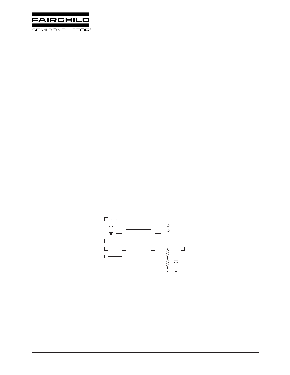
Typical Application
Input 1.6V
to 4.5V
ML4854
V
1
On
Off
Low Battery
Detect In
Low Battery
Detect Out
2
3
4
IN
SHDN
LBI
LB0
General Description
The ML4854 is a low power boost regulator designed for
low voltage DC to DC conversion in two-cell battery powered systems such as cell phones and PDAs. The converter
starts up at 1.3V and has an operating input voltage range
from 1.6V to 4.5V. After the start it operates at an input
voltage as low as 0.8V. Output voltage can be adjusted by
external resistors from 3.3V to 5V with a maximum load
current of 0.5A.
Quiescent current in shut down mode is less than 30µA,
which maximizes the battery live time. The ON time changes
with the input voltage to maintain the ripple current constant
and to provide the highest efficiency over a wide load range,
while maintaining low peak currents in the boost inductor.
The combination of integrated synchronous rectification,
variable frequency operation, and low supply current make
ML4854 ideal for portable applications.
The ML4854 is available in an 8 lead TSSOP package.
GND
8
7
V
L
6
V
OUT
5
FB
Output 3.3V to 5V
up to 0.5A
REV. 1.0.7 5/6/03
Page 2
PRODUCT SPECIFICATION ML4854
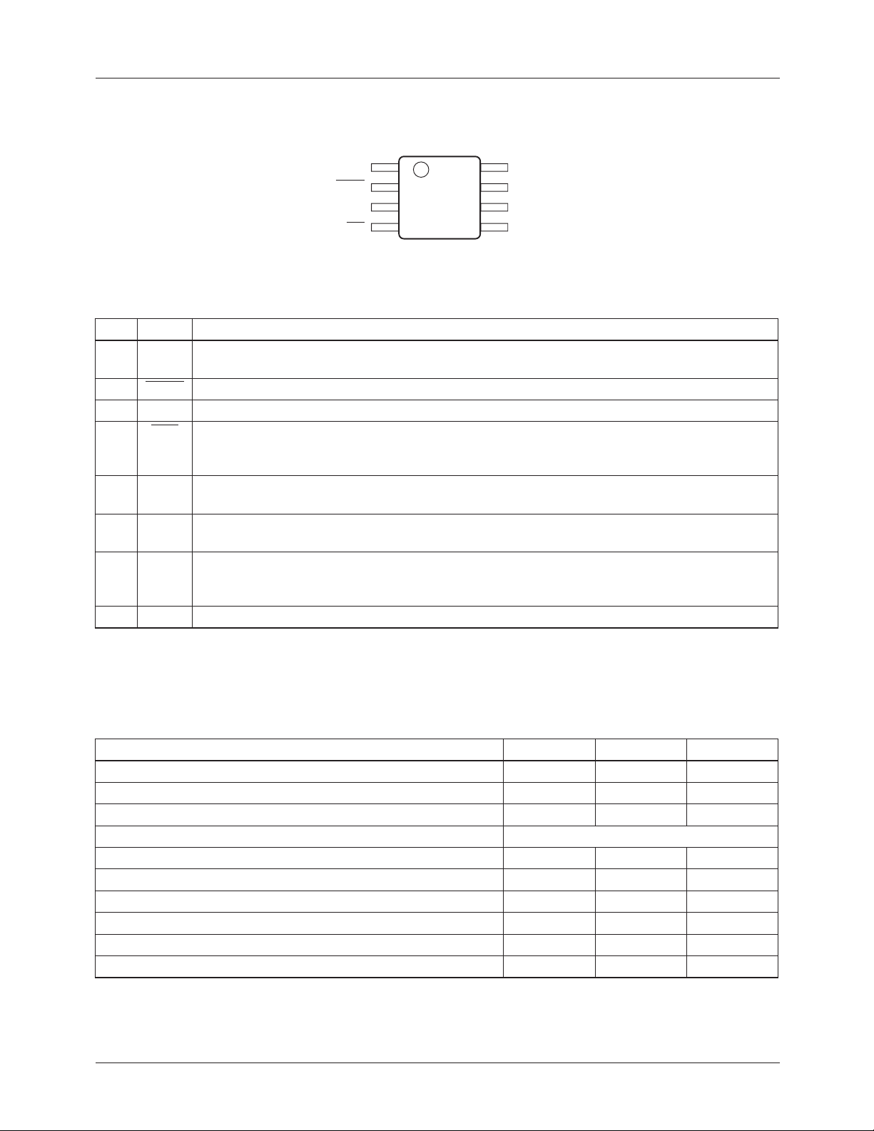
Pin Configuration
8-Lead TSSOP (T08)
V
SHDN
LBI
LB0
IN
1
2
3
4
TOP VIEW
Pin Description
PIN NAME FUNCTION
1 V
2 SHDN Shut Down . Pulling this pin low shuts down the regulator, isolating the load from the input.
3 LBI Low-Battery Input . Pulling this pin below a threshold causes the LBO pin to go low.
4 LBO Low-Battery Output . This pin provides an active low signal to alert the user when the LBI
5FB Programming Feedback Pin . Sets the output voltage. This pin is used to adjust the output
6V
OUT
7V
8 GND Ground of the IC .
Battery Input Voltage . Supplies the IC during start-up. After the output is running, the IC draws
IN
power from V
OUT
.
voltage falls below its targeted value. The open-drain output can be used to reset a
microcontroller.
voltage via a resistive divider from V
OUT
Boost regulator output . Output voltage can be set to be in the 3 to 5V range. Startup at
moderate load is achievable at input voltages around 1.25V.
Boost inductor connection . An inductor is connected between this pin and V
L
the output supply, this pin pulls low, charging the inductor, then shuts off dumping the energy
through the synchronous rectifier to the output.
8
7
6
5
GND
V
L
V
OUT
FB
.
. When servicing
IN
Absolute Maximum Ratings
Absolute maximum ratings are those values, beyond which the device could be permanently damaged. Absolute maximum
ratings are stress ratings only and functional device operation is not implied.
Parameter Min. Max. Units
,
V
V
IN
Switch Voltage (V
Voltage on any other Pin -0.3 V
Peak Switch Current (Ipeak) — Internally Limited —
Output Current (I
Continuous Power Dissipation 320 mW
Thermal Resistance ( θ
Junction Temperature 150 °C
Storage Temperature Range -65 +165 °C
Lead Temperature (soldering, 10s) 300 °C
2
Voltages (Relative to GND) -0.3 7 V
OUT
to GND) -0.3 V
L
) 500 mA
OUT
) 124 °C/W
JA
OUT
OUT
+0.3
+0.3
V
V
REV. 1.0.7 5/6/03
Page 3
µ
µ
µ
µ
µ
µ
µ
ML4854 PRODUCT SPECIFICATION
Recommended Operating Conditions
Parameter Min. Max. Units
Temperature Range -40 +85 °C
Operating Range
V
IN
Operating Range
V
OUT
1.6 0.9 V
OUT
3.0 5.0 V
V
Electrical Characteristics
Unless otherwise specified, V
at T
= +25°C
A
Parameter Conditions Min. Typ. Max. Units
Start Up Voltage I
Operating Voltage After start I
Output Voltage V
Output Voltage Adjust Range 3 5 V
Steady State Output Current
(see diagram)
Pulse Width V
Minimum Off-Time 0.5
Line Regulation V
Load Regulation 0 to 250mA V
Feedback Voltage (VFB) 1.230 V
LBI Threshold Voltage 0.390 V
LBI Hysteresys 25 mV
Internal NFET, PFET ON Resist. I
Efficiency (I
Quiescent Current – SHDN SHDN=0V, R1 excluded,V
LBO Output Voltage V
SHDN Input Voltage @V
SHDN Input Voltage @V
=1.6V to 3V, I
IN
=3V V
IN
=1.6V V
IN
=1mA, T
LOAD
<1mA 1.25 1.5 V
LOAD
LOAD
(nom.)=3.3V
OUT
V
(nom.)=5V
OUT
V
=3.3V, V
OUT
V
=5V, V
OUT
= 3V 0.8 1.32 1.9
IN
V
= 2.4V 1.2 1.64 2.3
IN
V
= 1.8V 1.8 2.15 3.1
IN
V
= 1.5V 2.2 2.57 4.0
IN
=1.6V to 3V, I
IN
V
=5V 0.5 %
OUT
0 to 150mA V
= 100mA 275 m Ω
LOAD
=200mA) V
LOAD
IN
=2.5V 330 mA
IN
IN
IN
SHDN=3V, R1 excluded,V
= 0, I
LBI
=3.3V/5V 1.6 V
OUT
=3.3V/5V 0.8 V
OUT
=1mA 0.2 V
SINK
=-40°C to +85°C. Test Circuit Fig.1. Typical values are
A
=10mA, V
=3.3V/5V 0.8 V
OUT
3.15
4.775
3.3
5
=2.5V 500 mA
=2mA, V
OUT
=2.4V ,V
=2.4V ,V
=3V, V
IN
OUT
OUT
=3.3V 0.5 %
OUT
=3.3V 1.0 %
=5V 1.0 %
= 3.3V 95 %
OUT
=3V 26 100
IN
=3V 85 200
IN
3.45
5.225
V
V
s
s
s
s
s
A
A
REV. 1.0.7 5/6/03
3
Page 4
PRODUCT SPECIFICATION ML4854
UP1B
L1
10uH
ML4854
100
Gnd
Vout
VL
FB
8
7
6
JP1
R6
287K
C3
18pF
C4
1.
0uF
R4
402K
R5
240K
J1
SCOPE JACK
+
C2
47uF
10V
VOUT
1
2
3.3V to 5.0V
C5
1uF
0.
GND1
1
2
VIN
2
1
1.6V to 3.0V
SHDN
2
1
Reset
2
1
Ext
Pull Up
2
1
GND
2
1
+
C1
47µF
R1
750K
R2
240K
JP2
JP3
U1
1
2
3
4 5
R3
100K
Vin
Shut down
LBI
LBO
Figure 1. Test Circuit
4
REV. 1.0.7 5/6/03
Page 5

ML4854 PRODUCT SPECIFICATION
Typical Operating Characteristics
Maximum Steady State Load
Current vs. Input Voltage
500
400
300
200
Max.Load Current, mA
100
1.5 2 2.5 3
100.0
90.0
80.0
70.0
60.0
50.0
40.0
Efficiency, %
30.0
20.0
10.0
0.0
Vin=3V
0.1 1 10 100 1000
= 3.3V
V
OUT
V
= 5V
OUT
Input Voltage, V
Efficiency vs. Load Current
Vout = 5V
Vin=2.0V
Output Current, mA
Vin=1.5V
(L=10µH, C
100.0
90.0
80.0
70.0
60.0
50.0
40.0
Efficiency, %
30.0
20.0
10.0
Output Voltage, V
=47µF, C
IN
Vin=3V
0.0
0.1 1 10 100 1000
Starting Up and Turning Off VOUT=3.3V
4
TURN OFF:
Iload=10mA
3.5
3
2.5
2
1.5
1
0.5
0
0 0.2
=47µF//1.0µF T=25°C)
OUT
Efficiency vs. Load Current
Vout = 3.3V
Vin=2.0V
Output Current, mA
Iload=10mA/50mA
0.4 0.6 0.8 1.0 1.2 1.4 1.6 1.8
Input (Battery) Voltage, V
load=50mA
Vin=1.5V
START UP
Iload=50mA
Iload=10mA
5
4
3
2
Output Voltage, V
1
0
0 0.2 0.4 0.6 0.8 1 1.2 1.4 1.6 1.8
REV. 1.0.7 5/6/03
Starting Up and turning Off VOUT=5V
Iload=10mA/50mA
TURN OFF:
Iload=10mA
load=50mA
Input (Battery) Voltage, V
START UP:
Iload=50mA
Iload=10mA
No-Load Battery Current vs. Input Battery
300
250
200
150
100
Battery Current, µA
50
0
0 1.2 1.4 1.6 1.8 2 2.2 2.4 2.6 2.8 3.0
Shut Down
Voltage
Vout=5V
Vout=3.3V
Battery Voltage, V
5
Page 6

PRODUCT SPECIFICATION ML4854
Typical Operating Characteristics
Line Transient Response @100mA Load
Exiting Shutdown
(Continued)
Inductor Current and Switching Node Voltage
Inductor
Current
V
L
Load Transient Response
I
LOAD
V
OUT
V
SHDN
Heavy-Load Switching Waveforms
V
L
I
L
V
OUT
V
OUT
6
REV. 1.0.7 5/6/03
Page 7

ML4854 PRODUCT SPECIFICATION
Typical Operating Characteristics
Output Voltage vs. Temperature
3.33
3.325
3.32
3.315
3.31
3.305
Output voltage, V
3.3
3.295
3.29
-50
Start-up Voltage vs. Load Current Switch ON Resistance vs. Temperature
1.8
1.6
Vout=5V
1.4
Start-up Voltage, V
1.2
1
0 50 100 150 200 250 300 -60
50mA
300 mA
0 50 100
Temperature, C
Vout=3.3V
Load Current, mA
(Continued)
Output Voltage,V
mohm
Switch Resistance,
Output Voltage vs. Temperature
5.09
5.08
5.07
5.06
5.05
5.04
5.03
5.02
-50 0 50 100
350
300
250
200
150
100
50
0
-40 -20 0 20 40 60 80 100
50 mA
200mA
Temperature, C
N-ch
P-ch
Temperature, C
500
450
400
350
300
250
200
150
100
Average Frequency, kHz
50
0
REV. 1.0.7 5/6/03
Operating Frequency, Vout=3.3V
f kHz @ I load=50 mA
f kHz @ I load=150 mA
f kHz @ I load=300 mA
f kHz @ I load=200 mA
f kHz @ I load=250 mA
SHDN Threshold Voltage vs. Input Voltage
2.5
2
1.5
1
SHDN Voltage (V)
0.5
0
001.522.533.5 12345
Input Voltage (V)Vin, V
7
Page 8

PRODUCT SPECIFICATION ML4854
Block Diagram
LBO
47
LBI
3
0.39V
V
IN
1
Functional Description
Minimum
Off-Time
Logic
–
A3
+
V
OUT
Start-Up
Variable
I
LIMIT
SHDN
On-Time
One Shot
Q
Boost regulator
ML4854 is an adjustable boost regulator that combines variable ON and minimum OFF architecture with synchronous
rectification. Unique control circuitry provides high-efficiency power conversion for both light and heavy loads by
transitioning between discontinuous and continuous conduction based on load conditions. There is no oscillator; a constant-peak-current limit of 1.5A in the switch allows the
inductor current to vary between this peak limit and some
lesser value. The switching frequency depends upon the load
and the input voltage, and can range up to 650kHz.
The input voltage (V
external Inductor to the V
V
closes through the external resistive voltage divider to
OUT
the feedback pin VFB. The transfer ratio of this divider determines the output voltage. When VFB voltage drops below
V
=1.23V, the error amplifier A1 signals to the regulator
REF
to deliver a charge to the output by triggering the Variable
On-Time One Shot. This generates a pulse at the gate of the
Power NMOS transistor Q1. This transistor will charge the
Inductor L1 for the time interval (TON) resulting in a peak
current given by:
I
L PEAK()
TONVIN×
---------------------------=
IN
L
1
) comes to V
pin of the device. The loop from
L
pin and through the
IN
V
L
I
LIMIT
Synchronous
Rectifier
Control
N1
1
When the one shot times out, the Q1 transistor releases the
VL pin, allowing the inductor to fly-back and momentary
charge the output through the body diode of the transistor
Q2. But, as the voltage across the Q2 changes polarity, its
gate will be driven low by the Synchronous Rectifier Control
Circuit (SRC), causing Q2 to short out its body diode. The
inductor then delivers the charge to the load by discharging
into it through Q2.
Under lightly loaded conditions, the amount of energy
delivered in this single pulse satisfies the voltage-control
loop, and the converter does not command any more energy
pulses until the output again drops below the lower-voltage
threshold. Under medium and heavy loads, a single energy
pulse is not sufficient to force the output voltage above its
upper threshold before the minimum off time has expired
and a second charge cycle is commanded. Since the inductor
current has not reached zero in this case, the peak current is
greater than the previous value at the end of the second
cycle. The result is a ratcheting of inductor current until
either the output voltage is satisfied, or the converter reaches
its set current limit.
After a period of time T
mum Off–Time Logic and if V
Variable On-Time One Shot will be turned ON again and the
process repeats.
The output capacitor of the converter (see Test circuit) filters
the variable component, limiting the output voltage ripple to
a value determined by its capacitance and its ESR.
Current
Limit
Control
REF
SHDN
2
V
OUT
6
V
FB
5
), the
Control
Logic
SHDN
Q
2
+
A2
–
I
LIMIT
–
A1
+
V
REF
8
GND
> 0.5µS, determined by Mini-
OFF
is low (VFB<V
OUT
8
REV. 1.0.7 5/6/03
Page 9

ML4854 PRODUCT SPECIFICATION
The synchronous rectifier significantly improves efficiency
without the addition of an external component, so that
conversion efficiency can be as high as 94% over a large load
range, as shown in the “Typical Operating Characteristics.”
Even at light loads, the efficiency stays high because the
switching losses of the converter are minimized by reducing
the switching frequency.
Error Detection Comparator (LBI – LBO)
An additional comparator A3 is provided to detect low VIN
or any other error conditions that is important to the user.
The non-inverting input of the comparator is internally
connected to a reference threshold voltage V
inverting input is connected to the LBI pin. The output of
the low battery comparator is a simple open-drain output
that goes active low if the battery voltage drops below the
programmed threshold voltage on LBI. The output requires a
pull-up resistor, with a recommended value of 100 kΩ, be
connected only to V
OUT
.
The low-battery detector circuit is typically used to supervise
the battery voltage and to generate an error flag or a RESET
command when the battery voltage drops below a user-set
threshold voltage. The function is active only when the
device is enabled. When the device is disabled, the LBO-pin
is high impedance.
while the
th
Setting the LBI Threshold of Low-Battery
Detector Circuit
The LBO-pin goes active low when the voltage on the
LBI-pin decreases below the set threshold typical voltage of
390 mV, which is set by the internal reference voltage.
The battery voltage, at which the detection circuit switches,
can be programmed with a resistive divider connected to
the LBI-pin. The resistive divider scales down the battery
voltage to a voltage level of tenths of volt, which is then
compared to the LBI threshold voltage. The LBI-pin has a
built-in hysteresis of 25 mV. The resistor values R1 and R2
can be calculated using the following equation:
V
= 0.39 x (R1+R2)/R2
IN_MIN
The value of R2 should be 270k or less to minimize bias current errors. R1 is then found by rearranging the equation:
R1=R2 x ( V
IN_MIN
/0.39 - 1)
If the low-battery detection circuit is not used, the LBI-pin
should be connected to GND (or to VIN) and the LBO-pin
can be left unconnected or tied to GND. Do not let the LBIpin float.
Component selection
Shutdown
The device enters shutdown when V
mately less than 0.5VIN). During shutdown the regulator
stops switching, all internal control circuitry including the
low-battery comparator is switched off and the load is
disconnected from the input. The output voltage may drop
below the input voltage during shutdown. The typical dependence shutdown voltage versus input voltage and the timing
process of the exiting shutdown are shown in the “Typical
Operating Characteristics.” For normal operation V
should be driven up 0.8VIN or connected to the VIN.
is low (approxi-
SHDN
SHDN
Application Information
Selecting the Output Voltage
The output voltage V
choosing resistors R4 and R5 of the divider in the feedback
circuit (see Test Circuit). The value of the R5 is recommended to be less than 270k. R4 can be calculated using
the following equation:
R4= R5[(V
where V
OUT/VREF
= 1.23V
REF
A compensation capacitor C3=18pF parallel with R4 provides better pulse grouping.
can be adjusted from 3V to 5V,
OUT
) – 1]
Output capacitor selection
The major parameter necessary to define the output capacitor
is the maximum allowed output voltage ripple of the converter. This ripple is determined by two parameters of the
capacitor, the capacitance and the ESR.
The contribution due to the capacitance can be determined
by looking at the change in capacitor voltage required to
store the energy delivered by the inductor in a single charge
–discharge cycle, as determined by the formula:
2
OUT
-----------------------------------------------------------=
2L× CV
∆V
T
ON
For example, if VIN=3V, V
2
V
×
IN
–()×
OUTVIN
OUT
=5V, L=10µH, TON =1.2µs,
C=47µF, the calculation by this formula gives an expected
output ripple due to only the capacitor value of 6.5mV.
In continuous inductor mode operation, this additional component of the ripple, due to capacitor ESR, can be calculated
using equation:
∆V
ESR
I
OUT
ESR()
-------------
×=
1D–
INtON
-------------------------+
2L
×
V
Where D is the duty cycle.
An additional ripple of 28 mV, at 100mA load current, is the
result of using a ceramic capacitor with an ESR of 70mΩ.
The total ripple is the sum of the ripple caused by the capacitance and the ripple caused by the ESR of the capacitor. In
this example, the total ripple is 34.5mV. It is possible to
REV. 1.0.7 5/6/03 9
Page 10

PRODUCT SPECIFICATION ML4854
improve the design by enlarging the capacitor or using
smaller capacitors in parallel to reduce the ESR or by using
better capacitors with lower ESR.
Tradeoffs have to be made between performance and costs of
the external parts of the converter circuit. For common, general purpose applications, a ceramic output capacitor with a
capacitance of 47µF and ESR less than 0.1Ω could be a good
choice. If a tantalum capacitor is used, a 100nF ceramic
capacitor in parallel, placed close to the IC, is recommended.
Input Capacitor Selection
Since the ML4854 does not require a large decoupling
capacitor at the input to operate properly, a 47µF capacitor is
sufficient for most applications requiring a good transient
response of the regulator. Optimum efficiency occurs when
the capacitor value is large enough to decouple the source
impedance. This usually occurs for capacitor values in
excess of 47µF.
Table 1. Recommended capacitors
Vendor Description
MuRata X5R Ceramic
AVX TAJ,TPS series tantalum
Sprague 595D series tantalum
Kemet T494 series tantalum
Inductor Selection
To select the boost inductor, it is necessary to keep the possible peak inductor current below the absolute peak current
limit of the power switch of the device. The highest peak
current through the inductor and the switch depends on the
load current (I
voltage (V
OUT
), the input voltage(VIN) and the output
LOAD
).
The maximum load current depends upon the inductance L,
according to the equation:
V
–
OUTVIN
VINI
I
LOADmax
------------------------------------------------------------------------------------
where, by design, t
–
LIMtOFFmin
OFFmin
efficiency η is usually 0.9. For VIN=3V, V
resulting I
LOADmax
will be around 0.4A.
------------------------------
V
OUT
= 0.5µS, I
2L
= 0.8A and the
LIM
OUT
=5V the
η×=
The second parameter for choosing the inductor is the
desired current ripple in the inductor. Normally, it is advisable to work with a ripple of less than 20% of the average
inductor current. A larger inductor value provides a smaller
ripple which reduces the magnetic hysteresis losses in the
inductor, as well as output voltage ripple and EMI. But in the
same way, regulation time at load changes will rise. Due to
the nature of the “go/no go” control, larger inductor values
typically result in larger overall voltage ripple, because once
the output voltage level is satisfied, the converter goes discontinuous, resulting in the residual energy of the inductor,
causing overshoot. The losses in the inductor caused by
magnetic hysteresis losses and copper losses are a major
parameter for total circuit efficiency. For better efficiency the
ESR of the inductor should be kept as low as possible. Lower
value inductors typically offer lower ESR and smaller
physical size.
An inductor value of 10 µH works well in most applications,
but values between 5 µH to 22 µH are also acceptable. A
MuRata LQ66C100M4, 10µH surface-mount inductor is
suitable, having a current rating of 1.6A and a max. ESR of
36 mΩ. Other choices for surface-mount inductors are
shown in Table 2.
Table 2. Recommended Inductors
Supplier Manufacturer Part Number
MuRata LQ66C100M4
Coilcraft DT1608C-103
Coiltronics UP1B100
Sumida CDR63B-100
Thermal considerations
Implementation of integrated circuits in low-profile surfacemount packages typically requires special attention to power
dissipation. Many system-dependent issues such as thermal
coupling, airflow, added heat sinks and convection surfaces,
and the presence of other heat-generating components affect
the power-dissipation limits of a given component.
Three basic approaches for enhancing thermal performance
are:
• Improving the power dissipation capability of the PCB
design
• Improving the thermal coupling of the component to the
PCB
• Introducing airflow in the system
The maximum junction temperature, T
J (MAX)
of the
ML4854 devices is 150°C. The thermal resistance of the
8-pin TSSOP package (T08) is θJA = 124°C/W. Specified
regulator operation is assured to a maximum ambient
temperature T
of 85°C. Therefore, the maximum
A(MAX)
power dissipation is about 320 mW. More power can be dissipated if the maximum ambient temperature of the application is lower, according to the relation:
P
D(MAX)
= [T
J(MAX)
–T
A(MAX)
] / θ
JA
Layout and Grounding
Considerations
Careful design of printed circuit board is recommended since
high frequency switching and high peak currents are present
in DC/DC converters applications. A general rule is to place
the converter circuitry well away from any sensitive analog
10 REV. 1.0.7 5/6/03
Page 11

ML4854 PRODUCT SPECIFICATION
components. The PCB layout should be based on some
simple rules to minimize EMI and to ensure good regulation
performances:
1. Place the IC, inductor, input and output capacitor as
close together as possible.
2. Keep the output capacitor as close to the ML4854 as
possible with very short traces to V
and GND pins.
OUT
Typically it should be within 0.25 inches or 6 mm.
3. Keep the traces for the power components wide,
typically > 50 mils or 1.25 mm.
4. Place the external networks for LBI and FB close to
ML4854, but as far away as possible from the power
components to prevent voltage transient from coupling
into sensitive nodes.
Application Example:
Using ML4854 as a constant current source to drive four LEDs:
Cin
+
1
2
3
4
+
L
ML4854
+
Cout
8
7
6
5
D1
D2
D3
R
R
R
5. On multilayer boards, use component side copper for
grounding around the IC and connect back to a quiet
ground plane using vias. The ground planes act as
electrostatic shields for some of the RF energy radiated.
6. The connection of the GND pin of the IC (pin 8) to the
overall grounding system should be directly to the
bottom of the output filter capacitor. A star grounding
system radiating from where the power enters the PCB,
is a recommended practice.
L = 10µH
Cin = Cout = 10µF
R = 62 ohm
D1...D4 = QTLP 600C-EB (blue)
D4
R
The current through the LEDs is maintained constant within a large input voltage range as shown in the diagram below:
ML4854 feeds LED QTLP 600C-EB
20
19.8
19.6
19.4
19.2
19
18.8
18.6
18.4
LED Current (mA)
18.2
18
01234
Input Voltage (V)
5
REV. 1.0.7 5/6/03 11
Page 12

PRODUCT SPECIFICATION ML4854
Mechanical Dimensions
Package: T08
8-Lead TSSOP
0.113 - 0.123
(2.87 - 3.12)
8
PIN 1 ID
0.033 - 0.037
(0.84 - 0.94)
1
0.026 BSC
(0.65 BSC)
0.008 - 0.012
(0.20 - 0.30)
SEATING PLANE
0.169 - 0.177
(4.29 - 4.50)
0.043 MAX
(1.10 MAX)
0.002 - 0.006
(0.05 - 0.71)
0.246 - 0.258
(6.25 - 6.55)
0°-8°
0.020 - 0.028
(0.51 - 0.71)
0.004 - 0.008
(0.10 - 0.20)
12 REV. 1.0.7 5/6/03
Page 13

PRODUCT SPECIFICATION ML4854
Ordering Information
Part Number Temperature Range Package
ML4854IT –40°C to 85°C 8 Pin TSSOP (T08)
DISCLAIMER
FAIRCHILD SEMICONDUCTOR RESERVES THE RIGHT TO MAKE CHANGES WITHOUT FURTHER NOTICE TO
ANY PRODUCTS HEREIN TO IMPROVE RELIABILITY, FUNCTION OR DESIGN. FAIRCHILD DOES NOT ASSUME
ANY LIABILITY ARISING OUT OF THE APPLICATION OR USE OF ANY PRODUCT OR CIRCUIT DESCRIBED HEREIN;
NEITHER DOES IT CONVEY ANY LICENSE UNDER ITS PATENT RIGHTS, NOR THE RIGHTS OF OTHERS.
LIFE SUPPORT POLICY
FAIRCHILD’S PRODUCTS ARE NOT AUTHORIZED FOR USE AS CRITICAL COMPONENTS IN LIFE SUPPORT DEVICES
OR SYSTEMS WITHOUT THE EXPRESS WRITTEN APPROVAL OF THE PRESIDENT OF FAIRCHILD SEMICONDUCTOR
CORPORATION. As used herein:
1. Life support devices or systems are devices or systems
which, (a) are intended for surgical implant into the body, or
(b) support or sustain life, and (c) whose failure to perform
when properly used in accordance with instructions for use
provided in the labeling, can be reasonably expected to
result in a significant injury of the user.
2. A critical component in any component of a life support
device or system whose failure to perform can be
reasonably expected to cause the failure of the life support
device or system, or to affect its safety or effectiveness.
www.fairchildsemi.com
5/6/03 0.0m 004
2003 Fairchild Semiconductor Corporation
Stock#DS30004854
 Loading...