

Datasheet ML4669CQ, ML4664CQ, ML4664IQ, ML4669IQ, ML4669CH Datasheet (Micro Linear Corporation)
...Page 1
July 2000
ML4664*/ML4669*
10BASE-FL to 10BASE-T Converter
GENERAL DESCRIPTION
The fully pin-compatible ML4664/ML4669 pair provide
FEATURES
■ Full duplex operation
conversion from 10BASE-T copper media to 10BASE-FL
fiber media in a single chip. They are compliant with
■ Five network status LED outputs
Ethernet IEEE 802.3 10BASE-T and 10BASE-FL standards.
The ML4664/69 uses a single 5V supply, and requires no
■ Industrial temperature option
crystal or clock.
10BASE-FL FEATURES:
Their 10BASE-FL transmitter offers a current drive output
that directly drives a fiber optic LED transmitter. Their
receiver offers a highly stable fiber optic data quantizer
capable of accepting input signals as low as 2mV
P-P
with
a 55dB dynamic range.
The 10BASE-T portion of the pair contains current driven
transmitter outputs that offer superior performance
■ Highly stable data quantizer with 55dB input dynamic
range
■ Input sensitivity as low as 2mV
■ Up to 100mA maximum current driven fiber optic LED
output for accurate launch power (PLCC package)
because their switching is highly symmetric, resulting in
lowered RFI noise and jitter. By changing one external
10BASE-T FEATURES:
resistor the pair easily interfaces to 100W unshielded
twisted pair, 150W shielded twisted pair, or a range of
■ Current driven output for low RFI noise and low jitter
other characteristic impedances.
■ Drives 100W unshielded or 150W shielded twisted pair
The ML4664 does not pass along disconnect information,
while the ML4669 does. A loss of light at the optical
■ Polarity detect status pin capable of driving an LED
inputs does not stop link pulses from being sent at the
twisted pair transmitter in the ML4664, but in the
■ Automatic polarity correction
ML4669 the link pulses stop. Also, a loss of link at the
twisted pair inputs will not stop the optical transmitter
■ On-chip link test with enable/disable option
from sending idle in the ML4664, but the ML4669 stops
sending idle. * Some Packages Are Obsolete
P-P
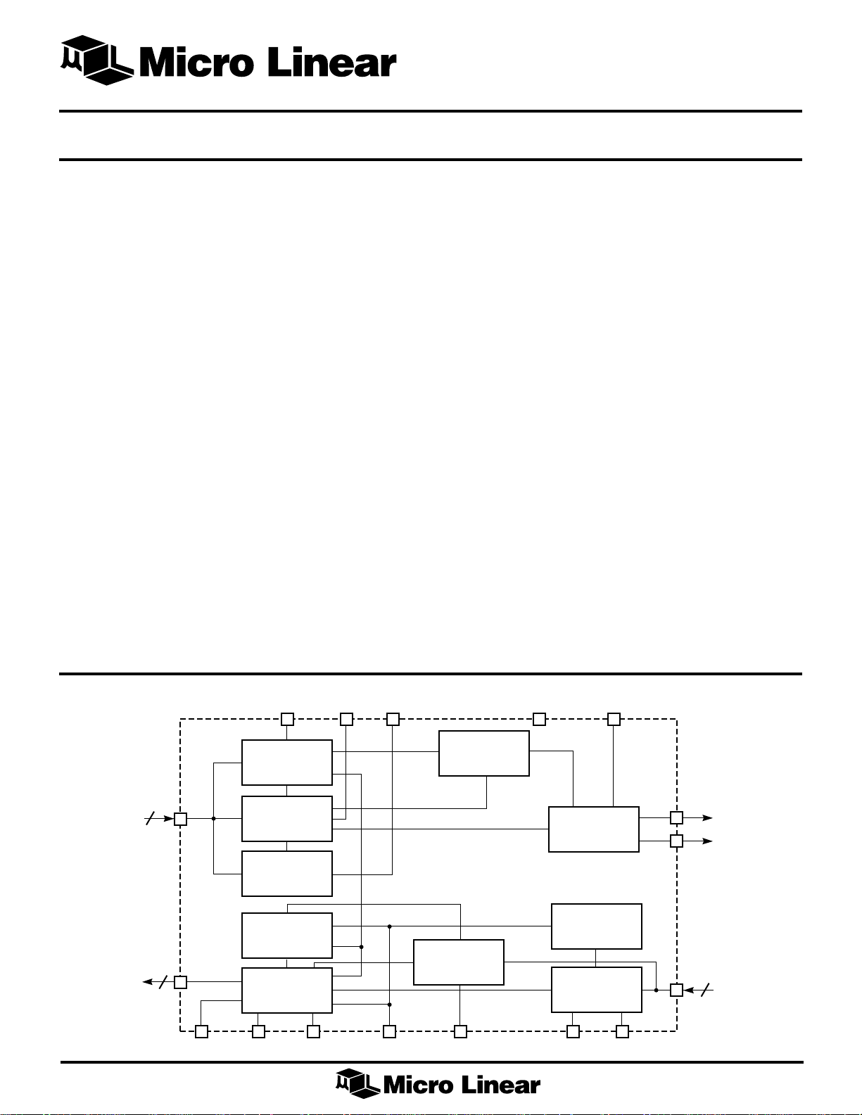
BLOCK DIAGRAM
TPIN
2
TPOUT
2
RTSETTP TxCAP0 TxCAP1
LINK PULSE
CHECK
RX SQUELCH
TP
POLARITY
CORRECT
LINK PULSE
GENERATOR
TP
TX
TPLED
RX SQUELCH
LMON
(LOW LIGHT)
IDLE
GENERATOR
TP
OPLED
OP
TX
THRESHOLD
GENERATOR
QUANTIZER
V
DC
RTSETOPRRSETPOLDISLTF
C
TIMER
OPOUT
OPVCC
2
OPIN
1
Page 2
ML4664/ML4669
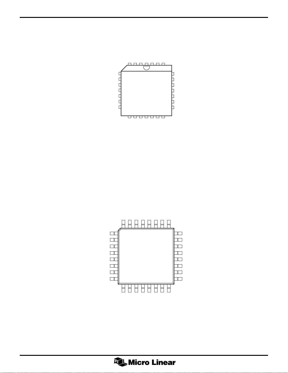
PIN CONFIGURATION
ML4664/ML4669
28-Pin PLCC (Q28)
TPINN
V
CC
TxCAP0
TxCAP1
GND
TPOUTN
TPOUTP
TPLED
LTF
CC
V
RTSETP
C
RRSET
TIMER
TPINP
4 3 2 1 28 27 26
5
6
7
8
9
10
11
12 13 14 15 16 17 18
POLDIS
TOP VIEW
OPLED
AVCCOPINP
LMON
RTSETOP
25
24
23
22
21
20
19
OPVCC
OPINN
AGND
V
THADJ
V
REF
V
DC
GND
OPOUT
TPINN
NC
V
CC
TxCAP0
TxCAP1
GND
TPOUTN
TPOUTP
ML4664/ML4669
32-Pin TQFP (H32-7)
TPLED
LTF
RTSETP
POLDIS
TOP VIEW
TIMER
C
OPLEDNCAVCCOPINP
CC
V
RRSET
RTSETOP
LMON
TPINP
32 31 30 29 28 27 26 25
1
2
3
4
5
6
7
8
9 10111213141516
NC
24
23
22
21
20
19
18
17
OPVCC
OPINN
AGND
V
THADJ
V
REF
V
DC
NC
GND
OPOUT
2
Page 3

ML4664/ML4669
PIN DESCRIPTION
PIN NAME FUNCTION
1(29) C
2(30) LTF Link Test Fail. Active high. Normally
3(31) TPLED Indicates that reception is taking place
4(32) TPINP Twisted Pair receive data input.
5(1) TPINN When this signal exceeds the
TIMER
A capacitor from this pin to V
determines the Link Monitor response
time.
this pin is low, indicating that the link
is operational. If the link goes down
resulting from the absence of link
pulses or frames being received, the
chip will go into the Link Test Fail
state and bring LTF high.
When the ML4664 is in the link test
fail state, the optical and twisted pair
transmitters are disabled from sending
data. However, the optical transmitter
does send an idle signal, and link
pulses are sent at the twisted pair
transmitter. When the ML4669 is in
link test fail state, the optical and
twisted pair transmitters are disabled
from sending data. Also, the optical
transmitter will not send an idle
signal. However, link pulses may be
sent at the twisted pair transmitter,
depending on the optical inputs. See
Table 1.
This pin may be grounded to disable
Link Test. In this mode no link pulses
are sent and the link will not fail if no
link pulses are received. If this pin is
not used as an LED driver, and is not
grounded, a 2kW 5% resistor should
be connected between this pin and
VCC.
on the TPINP, TPINN pair. Active low
LED driver, open collector. It is
extended 16ms for visibility.
Optionally, this pin may be grounded
to disable the optical output. If this
pin is not used as an LED driver and is
not grounded, a 2kW, 5% resistor
should be connected between TPLED
and VCC.
receive squelch requirements the
receive data is buffered and sent
to the Rx± outputs.
(Pin Number in Parentheses is for TQFP Version)
CC
PIN NAME FUNCTION
7(4) TxCAP0 An external capacitor of 680pF is
8(5) TxCAP1 tied between these two pins to set
the pulse width for the preequalization on the twisted pair
transmitter. If these two pins are
shorted together, no pre- equalization
occurs. If the ML4664/ML4669 is
driving only a short cable, or board
traces, these pins may be shorted.
9(6) GND Ground reference
20(18)
10(7) TPOUTN Pre-equalized differential balanced
11(8) TPOUTP current driven output. These outputs
are connected to a balanced transmit
output filter which drives the twisted
pair cable through pulse transformers.
The output current is set with an
external resistor connected to RTSET
allowing the chip to drive 100W
unshielded , 150W shielded twisted
pair cables or a range of other
characteristic impedances.
12(10) POLDIS Receive Polarity status. Active low
LED Driver, open collector output.
Indicates the polarity of the receive
twisted pair regardless of auto polarity
correction. When low, receive polarity
is reversed. When high, receive
polarity is correct. This pin may be
grounded to disable the polarity
circuit. If this pin is not used as an
LED driver, and is not grounded, a
2kW, 5% resistor should be connected
between this pin and VCC.
13(11) RTSETTP When using 100W unshielded twisted
pair, a 220W resistor is tied between
this pin and VCC. When using 150W
shielded twisted pair, a 330W resistor
is tied between this pin and VCC.
15(13) RRSET A 1% 61.9kW resistor tied from this
pin to VCC is used for internal biasing.
16(14) RTSETOP Sets the current driven output of the
transmitter. A 115W resistor should be
tied between this pin and VCC.
6(3) V
14(12)
CC
5V input
3
Page 4

ML4664/ML4669
PIN DESCRIPTION
PIN NAME FUNCTION
17(15) LMON Link Monitor “Low Light” LED status
output. Pulled low when voltage on
the OPINP, OPINN inputs exceed min
threshold set by V
transitions on OPINP, OPINN
indicating an idle signal or active
data. If the voltage on OPINP, OPINN
inputs falls below the minimum
threshold or transitions cease on
OPINP, OPINN, LMON will go high.
Active low LED driver, open collector.
In the low light state, optical and
twisted pair transmitters are disabled
from sending data. The optical
transmitter of the ML4664 does send
an idle signal, and link pulses are sent
at the twisted pair transmitter. For the
ML4669, the twisted pair transmitter
will not send link pulses, the optical
transmitter may send an idle signal,
depending on inputs. See Table 1.
18(16) OPVCC 5V supply for fiber optic
LED driver
19(17) OPOUT Fiber optic LED driver output
(Continued)
THADJ
, and there are
PIN NAME FUNCTION
22(21) V
23(22) V
24(23) AGND Analog Filtered Ground
25(24) OPINN This input pin should be capacitively
26(25) OPINP This input pin should be capacitively
27(26) AV
28(28) OPLED Indicates reception is taking place on
REF
THADJ
CC
A 2.5V reference with respect to GND
This input pin sets the link monitor
threshold
coupled to filtered AVCC. The input
resistance is approximately 1.3kW.
coupled to the input source. The input
resistance is approximately 1.3kW.
Analog Filtered 5V
the OPINP, OPINN pair. Active low
LED driver, open collector. It is
extended 16ms for usability. This pin
may be grounded to disable the
twisted pair outputs. If this pin is not
used as an LED driver, and is not
grounded, a 2kW, 5% resistor should
be connected between this pin and
VCC.
21(20) V
DC
An external capacitor on this pin
integrates an error signal which nulls
the offset of the input amplifier. If the
DC feedback loop is not being used,
this pin should be connected to V
REF
.
4
Page 5

ABSOLUTE MAXIMUM RATINGS
ML4664/ML4669
Absolute maximum ratings are those values beyond
which the device could be permanently damaged.
Absolute maximum ratings are stress ratings only and
Thermal Resistance (qJA)
PLCC ............................................................... 68°C/W
TQFP ............................................................... 80ºC/W
functional device operation is not implied.
OPERATING CONDITIONS
Power Supply Voltage Range
V
...................................................................GND –0.3 to 6V
CC
Input Voltage Range: Digital Inputs
(SQEN, LBDIS) ....................... GND –0.3 to VCC +0.3V
Tx+, Tx–, VIN+, VIN– .............. GND –0.3 to VCC +0.3V
Junction Temperature............................................. 150°C
Storage Temperature................................–65°C to 150°C
Lead Temperature (Soldering) ................................ 260°C
Temperature Range
ML4664/ML4669CX.................................. 0°C to 70°C
ML4664/ML4669IQ ...............................–40°C to 85°C
Supply Voltage (VCC) ......................................... 5V ± 5%
LED on Current ...................................................... 10mA
RRSET ........................................................ 61.9kW ± 1%
RTSETOP....................................................... 115W ± 1%
RTSETTP........................................................ 220W ± 1%
ELECTRICAL CHARACTERISTICS
Unless otherwise specified, TA = Operating Temperature Range, VCC = OPVCC = AVCC = 5V ± 5% (Note 1)
SYMBOL PARAMETER CONDITIONS MIN TYP MAX UNITS
I
CC
V
Power Supply Current RTSETOP = 115W 140 mA
While Transmitting
Reference Voltage C Suffix 2.30 2.60 V
REF
I Suffix 2.25 2.67 V
V
OL
I
OPOUT
I
TPOUT
V
TPSQ
H
TP
V
TPIN
R
TPIN
V
OPTH
H
OP
V
OPIN
R
OPIN
V
OPCM
A
V
V
OFF
V
N
I
TH
LED Drivers: V
OP Transmit Peak Output Current RTSETOP = 115 (Note 2) C Suffix 47 52 57 mA
TP Transmit Peak Output Current RTSETTP = 220 42 mA
TP Receive Squelch Voltage 300 450 585 mV
TP Receive Squelch Hysteresis 50 %
TP Receive Input Voltage 300 3100 mV
TP Receive Input Resistance 4 kW
OP Receive Input Threshold V
Voltage
OP Receive Input Threshold 20 %
Hysteresis
OP Receive Input Voltage 2 1600 mV
OP Receive Input Resistance 0.8 1.3 2.0 kW
OP Receive Common Mode 1.65 V
Voltage
Amplifier Gain 100 V/V
Input Offset VDC = V
Input Referred Noise 50MHz Bandwidth 25 µV
Input Bias Current at V
OL
THADJ
RL = 300 for OPLED, TPLED, 1.5 3.5 V
POLLED LTF, and LMON
I Suffix 46 58.5 mA
THADJ
V
THADJ
= V
REF
(DC Loop Inactive) 3 mV
REF
= V
REF
567mV
–200 0 200 µA
P-P
P-P
P-P
P-P
5
Page 6

ML4664/ML4669
ELECTRICAL CHARACTERISTICS
(Continued)
SYMBOL PARAMETER CONDITIONS MIN TYP MAX UNITS
OP TO TP (SEE FIGURE 1)
t
TPODY
t
TPSDY
t
TPSPW
t
Twisted Pair Start-up Delay 500 ns
Twisted Pair Steady State Delay 35 ns
Twisted Pair Turn Off Pulse Width 180 ns
Twisted Pair Jitter ±3.5 ns
PS
TP TO OP (SEE FIGURE 2)
t
OPODY
t
OPSDY
t
OPDI
1/t
P
IDC
t
OPJ
Optical Transmit Start-up Delay 500 ns
Steady State Delay 15 ns
Turn Off Width from Data to Idle 400 2100 ns
Idle Frequency 0.85 1.25 MHz
IDF
Idle Duty Cycle 45 55 %
Jitter into 31W Load ±1.5 ns
OPTICAL LINK VERIFICATION (SEE FIGURES 3-5)
t
OLL
No Light (No Transitions) to
LMON High 3 10 µs
t
OLM
Low Light (Below Threshold) to
LMON High 50 100 200 µs
t
OLO
Light On (Above Threshold, Transitions
<3µs) to LMON Low 0.25 0.5 0.75 s
TWISTED PAIR LINK VERIFICATION (SEE FIGURE 6)
t
t
LTMIN
t
LTMAX
Link Loss Time 50 150 ms
LT
Link Time Minimum 2 7 ms
Link Time Maximum 25 150 ms
LINK PULSE TRANSMIT (SEE FIGURE 7)
t
LPRR
t
LPW
Link Pulse Rep Rate 8 16 24 ms
Link Pulse Width 85 120 200 ns
LED TIMING (SEE FIGURE 8)
t
Note 1:
Note 2:
LED
LED on Time 8 16 32 ms
Limits are guaranteed by 100% testing, sampling, or correlation with worst-case test conditions.
The output current may be increased to 100mA by changing the RTSETOP resistor for the CQ (PLCC) package option only. See equation (1) on page 9. The increased
current option is not available for the CH (TQFP) package option.
6
Page 7

ML4664/ML4669
OPINP
OPINN
TPOUTP
TPOUTN
TPINP
TPINN
I(OPOUT)
t
OPODY
VALID
t
TPODY
DATA
VALID DATA
t
TPSDY
Figure 1. OP to TP Timing Diagram
t
OPSDY
Figure 2. TP to OP Timing Diagram
t
OPDI
t
TPSPW
t
IDF
OPINP
OPINN
LMON
OPINP
OPINN
LMON
t
OLL
Figure 3. Optical Link Verification No Light Timing Diagram
t
OLM
Figure 4. Optical Link Verification Low Light Timing Diagram
V
TH
7
Page 8

ML4664/ML4669
OPINP
OPINN
LMON
Figure 5. Optical Link Verification Light On Timing Diagram
TPINP
TPINN
VALID DATA OR LINK PULSE
LTF
t
OLO
t
LTMIN, tLTMAX
t
LT
TPINP
TPINN
TPOUTP
TPOUTN
TPINP, TPINN
OPINP, OPINN
Figure 6. Twisted Pair Link Verification Timing Diagram
t
LPW
t
LPRR
Figure 7. Link Pulse Transmit Timing Diagram
OR
VALID DATA
t
LED
TPLED
OR
OPLED
Figure 8. LED Timing Diagram
8
Page 9

SYSTEM DESCRIPTION
ML4664/ML4669
OPTICAL TRANSMISSION
The optical transmit function consists of detecting the
presence of data from the TP inputs TPINP and TPINN and
driving that data onto the fiber optic LED transmitter. A
positive signal on the TPINP lead relative to the TPINN
lead will result in no current, hence the fiber optic LED is
in a low light condition. When TPINP is more negative
than TPINN, the ML4664/ML4669 will sink current into
the chip and the fiber optic LED will light up.
Before data will be transmitted onto the fiber optic cable
it must exceed the squelch requirements. The TP inputs,
squelch circuit serves the function of preventing any noise
from being transmitted onto the fiber.
FIBER OPTIC LED DRIVER
The output stage of the transmitter is a current mode
switch which develops the output light by sinking current
through the LED into the OPOUT pin. Once the current
requirement for the LED is determined, the RTSETOP
resistor is selected. The following equation is used to
select the correct RTSETOP resistor:
RTSETOP
The ML4664/ML4669 optical transmitter (in the PLCC
package only) is capable of driving up to 100mA
maximum which requires resistor RSTETOP to equal 60W.
(This option is only available with the PLCC package) The
transmitter enters the idle state when it detects start of
idle on TPINP and TPINN input pins. After detecting the
start of idle the transmitter switches to a 1MHz output
idle signal.
=
52mA
I
OUT
´
115
W
(1)
2. All continuous sinusoidal signals of amplitude less
than 6.2V
3. All single sinusoidal cycles of amplitude less than
6.2V
P–P
between 2MHz and 15MHz. For a period of 4 BT
before and after this single cycle, the signal will
conform to (1) above.
4. All sinusoidal cycles gated by a 100ns pulse gate of
amplitude less than 6.2V
the sinusoidal frequency is between 2MHz and
30MHz. The off time of the pulse gate on the
sinusoidal signal shall be at least 400ns.
The first three receive squelch criteria are required to
conform to the 10BASE-T standard. The fourth receive
squelch criteria exceeds the 10BASE-T requirements and
enhances performance. The fourth squelch criteria
prevents a false unsquelch caused by cross talk or noise
typically found coupling from the phone lines onto the
receive twisted pair.
After the TP inputs are unsquelched, the detection
threshold is lowered to 225mV. Upon passing the TP
squelch requirements the receive data passes to the LED
Driver. The addition of jitter through the TP to OP path is
no more than ±1.5ns.
While in the unsquelch state, the TP squelch circuit looks
for the start of idle signal at the end of the packet. When
start of idle is detected, TP squelch is turned on again. The
proper start of idle occurs when the input signal remains
above 300mV for 160ns.
LINK TEST FUNCTION
and frequency less than 2MHz.
P–P
and either polarity, where the frequency is
and either polarity, where
P–P
The output current is switched through the OPOUT pin
during the on cycle and the OPVCC pin during the off
cycle. Since the sum of the current in these two pins is
constant, OPVCC should be connected as close as
possible to the VCC connection for the LED.
TP SQUELCH
The twisted pair receive data is transformer coupled and
low pass filtered before it is fed into the input pins TPINP
and TPINN. The input is differential with the common
mode voltage internally set. At the start of packet
reception from the twisted pair link, no more than 5 bits
are received from the twisted pair cable and not
transmitted. The first bit sent at the optical transmitter may
contain phase violations or invalid data, but all
subsequent bits are valid.
The TP squelch will reject the following signals on the
TPINP and TPINN inputs:
1. All signals that produce a peak magnitude less
than 300mV (450mV typical).
Transmission — Whenever data is not being delivered to
the twisted pair link, the idle signal is applied. The idle
signal is a sequence of Link Pulses separated by a 16ms
period of silence. The idle signal starts with a period of
silence after a packet transmission ends. The link test
pulse is a single high pulse with the same amplitude
requirements as the data signal.
Reception — The transceiver monitors the receive twisted
pair input for packet and link pulse activity. If neither a
packet nor a link test pulse is received for 50 to 150ms,
the transceiver enters the Link Test Fail state and inhibits
transmission and reception. Link pulses received with the
wrong polarity will be ignored and cause the chip to go
into link test fail.
When a packet, or five consecutive link test pulses is
received from the twisted pair input, the transceiver will
exit the Link Test Fail state upon transmit and receive data
being idle, and re-enable transmission and reception.
9
Page 10

ML4664/ML4669
SYSTEM DESCRIPTION
(Continued)
Link test pulses that do not occur within at most 25 to
150ms of each other are not considered consecutive.
In addition, detected pulses that occur within a time
between 2 to 7ms of a previous pulse will be considered
as noise by the link test circuitry, and will reset the count
of consecutive link pulses to zero.
If the ML4664 enters the link test fail state, both link
pulses at the twisted pair transmitter, and idle at the
optical transmitter will continue to be sent. Data will not
be sent at either transmitter.
If the ML4669 enters the link test fail state, idle will not
be sent at the optical transmitter. Data will not be sent at
either transmitter. However, link pulses may still be sent
at the twisted pair transmitter, depending on the optical
inputs. See Table 1.
POLARLITY CIRCUITRY
The ML4664/ML4669 offers automatic polarity correction.
The POLDIS pin is used to report the status of the receive
pair polarity. This pin is high when the polarity is correct,
and low when the polarity is reversed. If this pin is
grounded, the polarity correction circuit is disabled.
Polarity Detection — The internal circuitry uses the start
of idle signal to determine the receive polarity. With the
correct receive polarity, the Start of Idle signal (the end of
the frame) will remain above 300mV for more than
160ns. If the polarity is reversed, the Start of Idle signal
will end with a negative voltage.
The POLDIS status pin is updated only when four
consecutive frames are received with the same Start of
Idle polarity. In the case where the part is powered up
with the receive polarity reversed and no frames are
received, the part will go into link test fail without
reflecting a reverse polarity condition. If five consecutive
revised link pulses are then received, the polarity will
reverse and the device will come out of Link Test Fail.
TP TRANSMISSION
The TP transmit function consists of detecting the
presence of data from the OP inputs, OPINP and OPINN
and driving that data onto the transmit twisted pair
(TPOUTP, TPOUTN). A positive signal on the OPINP lead
relative to the OPINN lead will result in a positive signal
on the TPOUTP lead of the chip with respect to the
TPOUTN lead.
Before data will be transmitted onto the twisted pair from
the OP inputs, it must exceed the squelch requirements
for the OP inputs. The OP squelch circuit serves the
function of preventing any noise from being transmitted
onto the twisted pair.
The output stage of the transmitter is a current mode
switch which develops the output voltage by driving
current through the terminating resistor and the output
filter. The transmitter employs a center tap 2:1 transformer
where the center tap is tied to VCC (+5V). While one pin
of the transmit pair (TPOUTP, TPOUTN) is pulled low, the
other pin floats. The output pins to the twisted pair wires,
10
BINARY
TxTP+
TxTP–
OUTPUT AFTER
TRANSMIT FILTER
INPUT INTO
RECEIVER
011100110
Figure 9. Transmit Pre-Equalization Waveform
Page 11

ML4664/ML4669
SYSTEM DESCRIPTION
TPOUTP and TPOUTN, can drive a 100W, 150W load, or
a variety of impedances that are characteristic of the
twisted pair wire. RTSETTP selects the current into the
TPOUTP, TPOUTN pins. This current along with the
characteristic impedance of the cable determines the
output voltage.
Once the characteristic impedance of the twisted pair is
determined, one must select the appropriate RTSETTP
resistor as well as match the terminating impedances of
the transmit and receive filter. The RTSETTP resistor can
be selected as follows:
R
RTSETTP
Where RL is the characteristic impedance of the twisted
pair cable.
The transmitter incorporates a pre-equalization circuit for
driving the twisted pair line. Pre-equalization
compensates for the amplitude and phase distortion
introduced by the twisted pair cable. The twisted pair line
will attenuate the 10MHz signal more than the 5MHz
signal. Therefore pre-equalization insures that both the 5
and 10MHz components will be roughly the same
amplitude at the far end receiver.
L
=
100
220
W
(Continued)
(2)
While in the unsquelch state, the receive squelch circuit
looks for the start of idle signal at the end of the packet.
Start of idle occurs when the input signal remains idle for
more than 160ns. When start of idle is detected, the
receive squelch circuit returns to the squelch state and the
start of idle signal is output on the twisted pair outputs
TPOUTP, TPOUTN.
INPUT AMPLIFIER
The OPINP, OPINN input signal is fed into a limiting
amplifier with a gain of about 100 and input resistance of
1.3kW. Maximum sensitivity is achieved through the use
of a DC restoration feedback loop and AC coupling the
input. When AC coupled, the input DC bias voltage is set
by an on-chip network at about 1.7V. These coupling
capacitors, in conjunction with the input impedance of
the amplifier, establish a high pass filter with 3dB corner
frequency, fL, at:
f=
L
Since the amplifier has a differential input, two capacitors
of equal value are required. If the signal driving the input
is single ended, one of the coupling capacitors can be
tied to AV
1
2C
p
1300
.
CC
(3)
The pre-equalization circuit reduces the current output
when a 5MHz bit is being transmitted. After 50ns of a
5MHz bit, the current level is reduced to approximately
2/3 of its peak for the remaining 50ns. Figure 9 illustrates
the pre-equalization.
An on-chip one-shot determines the pulse width of the
pre-equalized transmit signal. This requires an external
capacitor connected to pins TxCAP0 and TxCAP1. The
proper value for this one-shot is 680pF. Pre-equalization
can be disabled by shorting TxCAP0 and TxCAP1 together.
The transmitter enters the idle state when it detects start
of idle on OPINP and OPINN input pins. The transmitter
maintains a minimum differential output voltage of at
least 450mV for 250ns after the last low to high transition.
The driver differential output voltage will then be within
50mV of 0V within 45 bit times.
OP SQUELCH
The input to the optical receiver comes from a fiber optic
pre-amp. At the start of packet reception no more than
2.7 bits are received from the fiber cable and not
transmitted onto the TP outputs. The receive squelch will
reject frequencies lower than 2.51MHz.
The internal amplifier has a lowpass filter built-in to band
limit the input signal which in turn will improve the
signal to noise ratio.
Although the input is AC coupled, the offset voltage
within
the amplifier will be present at the amplifier’s
output. In order to reduce this error a DC feedback loop
is incorporated. This negative feedback loop nulls the
offset voltage, forcing VOS to be zero. Although the
capacitor on VDC is non-critical, the pole it creates can
effect the stability of the feedback loop. To avoid stability
problems, the value of this capacitor should be at least 10
times larger than the input coupling capacitors.
The comparator is a high-speed differential zero crossing
detector that slices and accurately digitizes the receive
signal. The output of the comparator is fed into the
receive squelch circuit.
11
Page 12

ML4664/ML4669
R2
R1
V
THADJ
V
REF
Figure 10.
REF
THRESH
GEN
INPUTS OUTPUTS
STATUS LEDS
TPIN OPIN OPOUT TPOUT LTF
LMON
TPLED OPLED
None None None (Idle) None (LPS) OFF OFF OFF OFF
LPS None Idle None (LPS) ON OFF OFF OFF
Data None Idle None (LPS) ON OFF ON OFF
None Idle None (Idle) LPS OFF ON OFF OFF
LPS Idle Idle LPS ON ON OFF OFF
Data Idle Data LPS ON ON ON OFF
None Data None (Idle) LPS OFF ON OFF ON
LPS Data Idle Data ON ON OFF ON
Data Data Data Data ON ON ON ON
LPS = Link Pulses
ON = Low
OFF = High
Some simplifications made regarding LMON and LTF state machines, see system description.
Table 1. ML4669 Functionality. Differences in parentheses are for the ML4664.
12
Page 13

ML4664/ML4669
SYSTEM DESCRIPTION
(Continued)
OPTICAL LINK DETECT CIRCUIT AND LOW LIGHT
The link detect circuit monitors the input signal and
determines when the input falls below a preset voltage
level. When the input falls below a preset voltage, the
ML4664/ML4669 goes into the Low Light state. In the
Low Light state the TP transmitter is disabled, but
continues sending link pulses, the receiver is disabled,
and the LMON LED pin goes to high shutting off the
LMON LED. To return to the Link Pass state, the optical
receiver power must be 20% higher than the shut-off
state. This built-in hysteresis adds stability to the Link
Monitor circuit. Once the receiver power threshold is
exceeded, the ML4664/ML4669 waits 250ms to 750ms,
then checks to see that no data is being received before
re-enabling the transmitter, and receiver, and lighting up
the LMON LED.
When the ML4664 is in the low light state, both the link
pulses at the twisted pair transmitter and idle at the
optical transmitter continue to be sent. However, when
the ML4669 is in the low light state, link pulses are not
sent at the twisted pair transmitter. Data is not sent at
either transmitter. An idle signal may be sent at the
optical transmitter, depending on the twisted pair inputs.
See Table 1.
The V
pin is used to adjust the sensitivity of the
THADJ
receiver. The ML4664/ML4669 is capable of exceeding
the 10BASE-FL specifications for sensitivity. The sensitivity
is dependent on the layout of the PC board. A good low
noise layout will exceed the 10BASE-FL specifications,
while a poor layout will fail to meet the sensitivity and
BER spec.
The threshold generator shifts the reference voltage at
V
through a circuit which has a temperature
THADJ
coefficient matching that of the limiting amplifier. The
relationship between the V
and the VTH (the peak to
THADJ
peak input threshold) is:
case the Link Detect circuit must not disable the receiver
(i.e. V
of the receiver is determined, V
should be tied to 1.0V). Once the sensitivity
THADJ
can be set just
THADJ
above the power level that meets the BER specification.
This way the receiver will shut-off before the BER is
exceeded.
For 10BASE-FL V
can be tied directly to V
THADJ
REF
.
However if greater sensitivity is required the circuit in
Figure 10 can be used to adjust the V
if V
is tied to V
REF
, it is a good idea to layout a board
THADJ
voltage. Even
THADJ
with these two resistors available. This will allow
potential future adjustments without board revisions.
The response time of the Link Detect circuit is set by the
C
pin. Starting from the link off state the link can be
TIMER
switched on if the input exceeds the set threshold for a
time given by:
C
=
T
TIMER
0.7V
A700
m
(5)
To switch the link from on to off, the above time will be
doubled. A value of 0.05µF will meet to 10BASE-FL
specifications.
LED DRIVERS
The ML4664/ML4669 has five LED drivers. The LED driver
pins are active low, and the LEDs are normally off (except
for LTF and LMON). The LEDs are tied to their respective
pins through a 300W resistor to 5 Volts.
The OPLED and TPLED pins have pulse stretchers on
them which enables the LEDs to be visible. If another
event occurs before the timer expires, the LED timer will
reset and restart the timing. Therefore rapid events will
leave the LEDs continuously on. The LMON, LTF, and
POLDIS LEDs do not have a pulse stretcher on since its
condition occurs long enough for the eye to see.
VV
= 408
THADJ TH
(4)
A 10BASE-FL receiver must make less than 1 x 10–9 bit
errors at a receive power level of –32.5dBm average. One
procedure to determine the sensitivity of a receiver is to
start at the lowest optical power level and gradually
increase the optical power until the BER is met. In this
LOW LIGHT CONDITION
The LMON LED output is used to indicate a low light
condition. LMON is activated low when both the receive
power exceeds the Link Monitor threshold and there are
transitions on OPINP, OPINN less than 3µs apart. If either
one of these conditions do not exist, LMON will go high.
13
Page 14

ML4664/ML4669
V
CC
5V
C9
PWR
R12
510
33µF
* L1, L2: Fair-rite 2743019447
Ferrite beads
C8
0.1µF
L2*
L1**
+
C11
33µF
FILTERED
V
CC
C10
0.1µF
GND
P1
RJ45
14
3
12
6
19
1
17
2
VALOR
SF1301
OR
BEL
S556-2793-00
OR
EQUIVALENT
2:1 (TX)
1:1 (RX)
V
CC
R5
330Ω
TF
J2
2
V
CC
R14
8
7
9
2
3
4
50Ω
0.1µF
R15
200Ω
R16
200Ω
V
CC
220Ω
680pF
R3
C3
R13
50Ω
4
5
11
10
7
8
13
R6
330Ω
OP
J1 J4 J3
28 12 3 17
OPLED
LTF
TPINP
TPINN
TPOUTP
TPOUTN
TxCAP0
TxCAP1
RTSETTP
R7
330Ω
POL
DIS
POLDIS
ML4664
U1
92024
R4
330ΩR8330Ω
LMON
TP
TPLED
OPOUTP
AGNDGNDGND
#####
# Panasonic LNI4161C-(TR) LEDs
LMON
OPVCC
RTSETOP
RRSET
C
TIMER
V
DC
OPINN
OPINP
V
REF
V
THADJ
AV
CC
V
CC
V
CC
C12
0.1µF
V
CC
6
HFBR2416/
OPC2416
73
0.1µF
FILTERED
C6
0.1µF
2367
18
R17
1kΩ
HFBR1414/
OPC1414
R11
10Ω
2
1
4
5
6
19
R2
115Ω
16
R1
61.9kΩ
15
C1
0.047µF
1
C2
0.1µF
21
C5
0.01µF
25
C4
0.01µF
26
22
23
FILTERED
V
CC
27
6
V
CC
14
*R10: Optional to increase the sensitivity.
On this EVAL Board R9 is shorted and R10 is open.
R9
R10*
C7
V
CC
14
Figure 11. Typical Application Circuit.
Page 15

ML4664/ML4669
PHYSICAL DIMENSIONS
0.485 - 0.495
(12.32 - 12.57)
0.450 - 0.456
(11.43 - 11.58)
0.042 - 0.048
(1.07 - 1.22)
8
0.050 BSC
(1.27 BSC)
0.026 - 0.032
(0.66 - 0.81)
inches (millimeters)
1
PIN 1 ID
15
0.450 - 0.456
22
(11.43 - 11.58)
0.165 - 0.180
(4.06 - 4.57)
Package: Q28
28-Pin PLCC
0.485 - 0.495
(12.32 - 12.57)
0.148 - 0.156
(3.76 - 3.96)
0.042 - 0.056
(1.07 - 1.42)
0.009 - 0.011
(0.23 - 0.28)
0.025 - 0.045
(0.63 - 1.14)
(RADIUS)
0.099 - 0.110
(2.51 - 2.79)
0.300 BSC
(7.62 BSC)
0.390 - 0.430
(9.90 - 10.92)
1
0.013 - 0.021
(0.33 - 0.53)
0.354 BSC
(9.00 BSC)
0.276 BSC
(7.00 BSC)
PIN 1 ID
9
0.032 BSC
(0.8 BSC)
SEATING PLANE
32-Pin (7 x 7 x 1mm) TQFP
25
0.012 - 0.018
(0.29 - 0.45)
Package: H32-7
0.276 BSC
(7.00 BSC)
17
0.354 BSC
(9.00 BSC)
0.037 - 0.041
(0.95 - 1.05)
0.048 MAX
(1.20 MAX)
0º - 8º
0.003 - 0.008
(0.09 - 0.20)
0.018 - 0.030
(0.45 - 0.75)
SEATING PLANE
15
Page 16

ML4664/ML4669
ORDERING INFORMATION
PART NUMBER TEMPERATURE PACKAGE
ML4664CH (Obsolete) 0°C to 70°C 32–Pin TQFP(H32-7)
ML4664CQ 0°C to 70°C Molded 28–Pin PLCC (Q28)
ML4664IQ (Obsolete) –40°C to 85°C Molded 28–Pin PLCC (Q28)
ML4669CH 0°C to 70°C 32–Pin TQFP(H32-7)
ML4669CQ 0°C to 70°C Molded 28–Pin PLCC (Q28)
ML4669IQ (Obsolete) –40°C to 85°C Molded 28–Pin PLCC (Q28)
© Micro Linear 1998. is a registered trademark of Micro Linear Corporation. All other trademarks are the property of their respective owners.
Products described herein may be covered by one or more of the following U.S. patents: 4,897,611; 4,964,026; 5,027,116; 5,281,862; 5,283,483;
5,418,502; 5,508,570; 5,510,727; 5,523,940; 5,546,017; 5,559,470; 5,565,761; 5,592,128; 5,594,376; 5,652,479; 5,661,427; 5,663,874; 5,672,959;
5,689,167; 5,714,897; 5,717,798; 5,742,151; 5,747,977; 5,754,012; 5,757,174; 5,767,653; 5,777,514. Japan: 2,598,946; 2,619,299; 2,704,176.
Other patents are pending.
Micro Linear reserves the right to make changes to any product herein to improve reliability, function or design. Micro Linear does not assume any
liability arising out of the application or use of any product described herein, neither does it convey any license under its patent right nor the rights of
others. The circuits contained in this data sheet are offered as possible applications only. Micro Linear makes no warranties or representations as to
whether the illustrated circuits infringe any intellectual property rights of others, and will accept no responsibility or liability for use of any application
herein. The customer is urged to consult with appropriate legal counsel before deciding on a particular application.
16
DS4664_69-01
2092 Concourse Drive
San Jose, CA 95131
Tel: 408/433-5200
Fax: 408/432-0295
www.microlinear.com
8/28/98 Printed in U.S.A.
 Loading...