

Page 1

November 1998
ML4658
10BASE-T Transceiver
GENERAL DESCRIPTION
The ML4658 10BASE-T Transceiver is a single chip cable
line driver/receiver that provides all of the functionality
required to implement both an internal and external IEEE
802.3 10BASE-T MAU. This part offers a standard IEEE
802.3 AU interface that allows it to directly connect to
industry standard manchester encoder/decoder chips or to
an AUI cable.
The ML4658 requires a minimal number of external
components, and is compliant to the IEEE 802.3 10BASE-T
standard. The differential current driven transmitter offers
superior performance because of its highly symetrical
switching. This results in low RFI noise and low jitter.
The Transceiver easily interfaces to 100Ω unshielded
twisted pair cable, 150Ω shielded twisted pair cable, or a
range of other characteristic impedances by simply
changing one external resistor. Jabber, Link Test, and SQE
Test are fully integrated onto the chip with enable/disable
options. A polarity detection status pin, which can drive
an LED, is provided for receive data, and the ML4658
offers automatic polarity correction.
BLOCK DIAGRAM
FEATURES
■ Complete implementation of IEEE 802.3 10BASE-T
Medium Attachment Unit (MAU)
■ Incorporates an AU interface for use in an external
MAU or internal MAU
■ Single 5V supply ±10%
■ No crystal or clock input
■ Current Driven Output for low RFI noise and low jitter
■ Capable of driving 100Ω unshielded twisted pair cable
or 150Ω shielded twisted pair cable
■ Polarity detect status pin capable of driving an LED
■ Automatic Polarity Correction
■ On-chip Jabber logic, Link Test, and SQE test with
enable/disable option
■ Provides six network status LED ouput pins
Tx+
Tx–
COL+
COL–
Rx+
Rx–
AUI
RECEIVER
TRANSMIT
SQUELCH
AUI
DRIVER
AUI
DRIVER
GND
V
CC
SQEN/LTD/JABD
10MHz GATED
OSCILLATOR
LOOPBACK
MUX
(
5V)
5V
SQE
RRSET
5V
RTSET
LINK PULSE
TxTP+
PRE-EQUALIZED
TRANSMIT DRIVER
JABBER
RECEIVE
SQUELCH
LINE
RECEIVER
Tx
Rx
LINK TEST
RECEIVE LOGIC
LED DRIVERS
CLSN JAB RCV LTFXMT POLRD
AUTOMATIC
POLARITY
CORRECTION
TxTP–
TxCAP0
TxCAP1
RxTP+
RxTP–
BIAS
1
Page 2
ML4658
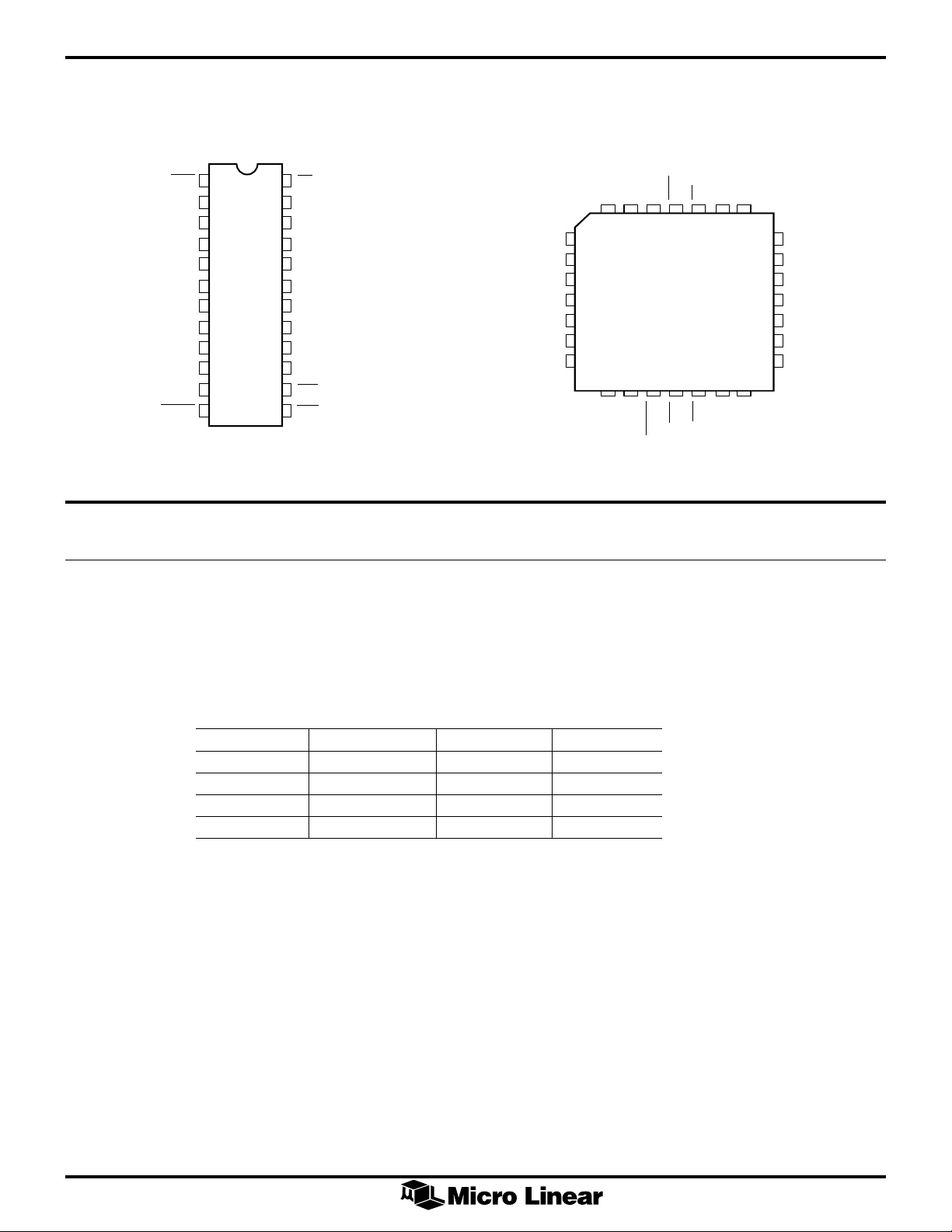
PIN CONFIGURATION
ML4658
24-Pin DIP
ML4658
28-Pin PCC
CLSN
COL+
COL–
SQEN/LTD/JABD
Rx+
Rx–
V
CC
Tx+
Tx–
RTSET
RRSET
POLRD
1
2
3
4
5
6
7
8
9
10
11
12
TOP VIEW
JAB
24
COL–
BIAS
23
RxTP+
22
RxTP–
21
LTF
20
TxCAP0
19
TxCAP1
18
GND
17
TxTP+
16
TxTP–
15
RCV
14
XMT
13
NC
Rx+
Rx–
V
V
Tx+
Tx–
CC
CC
SQEN/LTD/JABD
4 3 2 1 28 27 26
5
6
7
8
9
10
11
12 13 14 15 16 17 18
RTSET
COL+
RRSET
POLRD
TOP VIEW
CLSN
XMT
JAB
RCV
BIAS
TxTP–
RxTP+
25
24
23
22
21
20
19
TxTP+
RxTP–
LTF
NC
TxCAP0
TxCAP1
GND
GND
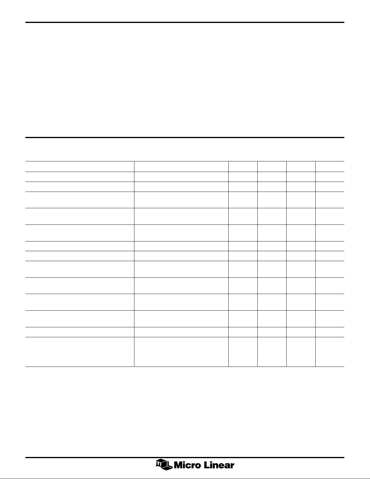
PIN DESCRIPTION (DIP)
PIN# NAME FUNCTION
1 CLSN Indicates that a collision is taking place. Active low LED driver, open collector. Event is extended
100ms for visibility.
2 COL+ Gated 10MHz signal used to indicate a collision, SQE test, or jabber. Balanced differential
3 COL– line driver outputs that meet AU interface specifications. AC or DC coupled.
4 SQEN/LTD/ SQE Test Enable, Link Test Disabled, Jabber Disabled. This input uses four voltage levels to
JABD configure the chip as shown in Table 1.
Table 1. SQEN/LTD/JABD Pin Configuration
Pin SQE Test Link Test Jabber
0V (GND) Disabled Enabled Enabled
1.2V Disabled Disabled Disabled
BIAS Enabled Disabled Enabled
5V (VCC) Enabled Enabled Enabled
When link test is disabled, no link pulses are transmitted, and the transmitter and receiver will not be
disabled as a result of a loss of receive link pulses. When Jabber is disabled the transmitter can
transmit continuously without interruption, and the collision oscillator will not be activated.
5 Rx+ Manchester encoded receive data output to the local device. Balanced differential line driver outputs
6 Rx– that meet AU interface specifications. AC or DC coupled.
7V
CC
5 Volt power input.
8 Tx+ Balanced differential line receiver inputs that meet AU interface specifications. These inputs may be
9 Tx– AC or DC coupled. When AC coupled, the BIAS pin is used to set the common mode voltage. Signals
meeting the transmitter squelch input requirements are pre-equalized and output on TxTP+ and TxTP–.
10 RTSET When using 100Ω unshielded twisted pair, a 220Ω resistor is tied between this pin and VCC. When
using 150Ω shielded twisted pair, a 330Ω resistor is tied between this pin and VCC.
1 1 RRSET A 1% 61.9KΩ resistor tied from this pin to VCC is used for internal biasing.
2
Page 3

ML4658
PIN DESCRIPTION (DIP)
PIN# NAME FUNCTION
12 POLRD Receive Polarity status. Active low LED Driver, open collector output. Indicates the polarity of the
receive twisted pair regardless of auto polarity correction. When this pin is high, the receive polarity
is correct, and when this pin is low the receive polarity is reversed.
13 XMT Indicates that transmission is taking place on the TxTP+, TxTP– pair. Active low LED driver, open
collector. It is extended 100ms for visibility.
14 RCV Indicates that the transceiver has unsquelched and is receiving data from the twisted pair. Active low
LED driver, open collector. It is extended 100ms for visibility.
15 TxTP– Pre-equalized differential balanced current driven output. These ouputs are connected to a balanced
16 TxTP+ transmit output filter which drives the twisted pair cable through pulse transformers. The output current
is set with an external resistor connected to RTSET allowing the chip to drive 100Ω unshielded twisted
pair, 150Ω shielded twisted pair cables or a range of other characteristic impedances.
17 G N D Ground reference.
18 TxCAP1 An external capacitor of 330pF is tied between these two pins to set the pulse width for the pre-
19 TxCAP0 equalization on the transmitter. If these two pins are shorted together, no pre-equalization occurs.
20 LTF Link Test Fail. Active high. Normally this pin is low, indicating that the link is operational. If the link
goes down resulting from the absence of link pulses or frames being received, the chip will go into
the Link Test Fail state and bring LTF high. In the Link Test Fail state, both the transmitter and receiver
are disabled, however link pulses are still sent. A station that only has access to the AUI can detect a
Link Test Fail by the absence of loopback. This pin is low when the Link Test is disabled. Open
collector LED output.
(Continued)
21 RxTP– Twisted Pair receive data input. When this signal exceeds the receive squelch requirements the
receive
22 RxTP+ data is buffered and sent to the Rx± outputs.
23 BIAS Bias voltage, output. Used to bias the receive twisted pair inputs as well as the Tx± inputs when they
are AC coupled.
24 JAB Open collector TTL output capable of driving an LED. When in the Jabber state, this pin will be low
and the transmitter will be disabled. In the Jabber “OK” state this pin will be high.
3
Page 4
ML4658
ABSOLUTE MAXIMUM RATINGS (Note 1)
Power Supply Voltage Range
V
...............................................................................–0.3 to 6V
CC
Input Voltage Range
Digital Inputs (SQEN, LTD)........................ –0.3 to V
Tx+, Tx–, RxTP+, RxTP– ............................ –0.3 to V
CC
CC
OPERATING CONDITIONS
Supply Voltage (VCC).........................................5V ±10%
LED on Current....................................................... 10mA
RRSET ......................................................... 61.9KΩ ±1%
RTSET ............................................................ 220Ω ±1%
TxC AP....................................................................330pF
Input Current
RRSET, RTSET, JAB, CLSN, XMT, RCV, LTF .......... 60mA
Output Current
TxTP+, TxTP–...................................................... 80mA
Storage Temperature................................ –65°C to 150°C
Lead Temperature (Soldering 10 sec.) .....................260°C
ELECTRICAL CHARACTERISTICS
Unless otherwise specified, TA = 0°C to 70°C (Note 3), VCC = 5V ±10% (Note 2)
PARAMETER CONDITIONS MIN TYP MAX UNITS
Power Supply Current ICC (Note 4) VCC = 5V 14 0 mA
LED Drivers: V
Transmit Peak Output Current RTSET = 220Ω 42 mA
Transmit Squelch Voltage Level
(Tx+, Tx–) –170 mV
Differential Input Voltage
(RxTP+, RxTP–) ±0.300 ±3.1 V
Receiver Input Resistance 10 kΩ
SQEN/LTD/JABD Input Resistance 12 kΩ
Receive Squelch Voltage Level
(RxTP+, RxTP–) 300 450 585 mV-p
Differential Output Voltage
(Rx±, COL±) ±550 ±1200 mV
Common Mode Output Voltage
(Rx±, COL±) 4.0 V
Differential Output Voltage Imbalance
(Rx±, COL±) 2 ±40 mV
BIAS Voltage 3.2 V
SQEN/LTD/JABD SQE TEST disabled 0.3 V
OL
RL = 510Ω (Note 5) 0.8 V
(Note 6)
All disabled 1.1 1.4
Link Test Disabled BIAS – 0.15 BIAS + 0.15
All Enabled VCC – 0.05V
Note 1: Absolute maximum ratings are limits beyond which the life of the integrated circuit may be impaired. All voltages unless otherwise specified are measured with
respect to ground.
Note 2: Limits are guaranteed by 100% testing, sampling, or correlation with worst-case test conditions.
Note 3: Low Duty cycle pulse testing is performed at T
Note 4: This does not include the current from the AUI pull down resistors, the transmit pins TxTP+ and TxTP– or the LED output pins.
Note 5: LED drivers can sink up to 20mA, but VOL will be higher.
Note 6: This current will result in a 2.5V peak output voltage on unshielded twisted pair cable when connected through an external filter and transformer as shown in Figure 12.
.
A
4
Page 5
ML4658
ELECTRICAL CHARACTERISTICS (Continued)
AC ELECTRICAL CHARACTERISTICS
SYMBOL PARAMETER MIN TYP MAX UNITS
Transmit
t
TXNPW
t
TXFPW
t
TXLP
t
TXODY
t
TXSDY
t
TXJ
Receive
t
RXODY
t
RXTDY
t
RXFX
t
RXSDY
t
RXJ
t
AR
t
AF
Collision
t
CPSQE
t
TXRX
t
SQEXR
t
SQEXT
t
CLF
t
CLPDC
t
SQEDY
t
SQETD
Jabber, Link Test and LED Timing
t
JAD
t
JRT
t
JSQE
t
LLT
t
LTN
t
LTX
t
TLP
t
LTPW
t
LEDT
Transmit Turn-On Pulse Width 20 n s
Transmit Turn-Off Pulse Width 18 0 ns
Transmit Loopback Startup Delay 200 ns
Tranmitter Turn-On Delay 200 ns
Transmit Steady State Prop. Delay 15 100 ns
Transmitter Jitter ±2 ±3.5 ns
Receive Turn-On Delay if Transmit is Idle 420 500 ns
Receive Turn-On Delay if Tranmit is Active 650 800 ns
Last Bit Received to Start Slow Decay Output 230 800 ns
Receive Steady State Prop. Delay 15 100 ns
Receiver Jitter ±0.7 ±1.5 ns
Differential Output Rise Time 20% to 80% (Rx±, COL±) 3 ns
Differential Output Fall Time 20% to 80% (Rx±, COL±) 3 ns
Collision Present to SQE Assert 0 900 ns
Time for Loopback to swtich from Tx to RxTP
during a collision 0 900 ns
Time for SQE to deactivate given that RxTP goes idle and
TxTP continues 0 90 0 n s
Time for SQE to deactivate given that TxTP goes idle
and RxTP continues 0 90 0 n s
Collision Frequency 8.5 10 11.5 MHz
Collision Pulse Duty Cycle 40 50 60 %
SQE Test Delay (Tx Inactive to SQE) 0.6 1.1 1.6 µs
SQE Test Duration 0.5 1.0 1.5 µs
Jabber Activation Delay 20 70 150 ms
Jabber Reset Unjab Time 250 450 750 ms
Delay from Outputs Disabled to Collision Oscillator On 100 ns
Link Loss Time 5 0 95 150 ms
Link Test Pulse Receive Minimum Time 2 4.2 7 ms
Link Test Pulse Receive Maximum Time 25 70 150 ms
Link Test Pulse Repetition Rate 8 16 24 ms
Link Test Pulse Width 85 100 200 ns
XMT, RCV, CLSN On Time 30 100 300 ms
5
Page 6
ML4658
TIMING DIAGRAMS
Tx+
Tx–
TxTP+
TxTP–
Rx+
Rx–
t
TXNPW
VALID DATA
t
TXODY
t
TXLP
t
TXSDY
VALID DATA
DATAVALID
Figure 1. Transmit and Loopback Timing
t
TXFPW
RxTP+
RxTP–
Rx+
Rx–
t
RXODY
t
RXTDY
VALID DATA
t
RXSDY
t
RXFX
t
AR
DATAVALID
t
AF
Figure 2. Receive Timing
6
Page 7

TIMING DIAGRAMS (Continued)
TxTP+
TxTP–
RxTP+
RxTP–
t
CPSQE
COL+
COL–
Rx+
Rx–
Tx Tx Tx RxTPRxTP RxTP
VALID DATA
VALID DATA
t
TXRX
ML4658
CS0
RxTP+
RxTP–
TxTP+
TxTP–
COL+
COL–
RxTP+
RxTP–
TxTP+
TxTP–
t
CPSQE
VALID DATA
VALID DATA
VALID DATA
CS0
Figure 3. Collision Timing
COL+
COL–
Rx+
Rx–
t
SQEXR
CS0
RxTP RxTP Tx Tx Tx Tx
Figure 4. Collision Timing
7
Page 8

ML4658
TIMING DIAGRAMS (Continued)
TxTP+
TxTP–
RxTP+
RxTP–
COL+
COL–
Rx+
Rx–
COL+
COL–
VALID DATA
t
SQEXT
CS0
RxTP RxTP RxTP RxTP RxTP
1
t
CLF
Figure 5. Collision Timing
Tx+
Tx –
TxTP+
TxTP–
COL+
COL–
TxTP+
TxTP–
COL+
COL–
VALID DATA
Figure 6. SQE Timing
VALID DATA
t
JAD
VALID
DATA
t
SQEDY
t
JSQE
CS0
t
SQETD
t
JRT
CS0
Figure 7. Jabber Timing
8
Page 9

TIMING DIAGRAMS (Continued)
ML4658
RxTP+
RxTP–
RxTP+
RxTP–
LTF
RxTP+
RxTP–
TxTP+
TxTP–
RECEIVER FRAME
LINK PULSE
t
, t
LTN
LTX
t
TLP
t
LTPW
Figure 8. Link Pulse Timing
t
LLT
TRANSMIT, RECEIVER
LOOPBACK DISABLE
TxTP+
TxTP–
XMT
RxTP+
RxTP–
RCV
t
LEDT
Figure 9. LED Timing
t
LEDT
9
Page 10

ML4658
SYSTEM DESCRIPTION
Figure 10 shows a typical block diagram of an external
10BASE-T transceiver interface. On one side of the
transceiver is the AU interface and the other is the twisted
pair. The AU interface is AC coupled when used in an
external transceiver or can be AC or DC coupled when
used in an internal transceiver. The AU interface for an
external transceiver includes isolation transformers, some
biasing resistors, and a voltage converter for power.
The twisted pair side of the transceiver requires external
transmit and receive filters, isolation transformers, and
terminating resistors. These components can be obtained
in a single hybrid package from suppliers listed in Figure
12. The transmitter sends pre-equalized data through the
transmit filters onto the twisted pair. The pre-equalized
data uses a standard two step output waveform that lowers
the amplitude of the 5MHz component so that at the
receiving end both the 5MHz and 10MHz components
have the same amplitude. The external transmit filter
smooths the edges of the signal before passing it onto the
twisted pair.
The receive pair side of the transceiver accepts the data
after it passes through the isolation transformer and the
receive low pass filter. Since this is an AC coupled input,
the Bias pin is used to set the proper common mode
voltage for the receive inputs. A pair of 50Ω resistors
correctly terminate the receive pair and provide a
common mode for the Bias voltage connection point.
AU INTERFACE
The AU interface consists of 3 pairs of signals, DO, CI and
DI, as shown in Figure 10. The DO pair contains transmit
data from the DTE which is received by the transceiver
and sent out onto the twisted pair. The DI pair contains
valid data that has been either received from the twisted
pair or looped back from the DO and output through the
Dl pair to the DTE. The CI pair indicates whether a
transmit based collision has occurred. It is an output that
oscillates at 10MHz. CI pair is also used for Jabber and
SQE Test.
The transceiver may be AC or DC coupled depending on
the application. For the AC coupled interface, the DO
input must be DC biased (shifted up in voltage) for the
proper common mode input voltage. The BIAS pin serves
this purpose. When DC coupled, the manchester encoder/
decoder transmit output pair provides this common mode
voltage and the Bias pin is not connected.
The two 39Ω 1% resistors tied to the Tx+ and Tx– pins
serve two purposes. They provide a point to connect the
common mode bias voltage, and they provide the proper
matching termination for the AUI cable. The CI and DI
pair, which are output drivers from the transceiver to the
AUI cable, require 360Ω pull down resistors when
terminated with a 78Ω load. However on a DTE card, CI
and DI do not need 78Ω terminating resistors. This also
means that the pull down resistors on CI and DI can be
1kΩ or greater depending upon the particular manchester
encoder/decoder chip used.
39Ω
360Ω
360Ω
D0
C1
D1
360Ω
360Ω
+5V
V
TxIN+
TxIN–
39Ω
COL+
COL–
RxOUT+
RxOUT–
CC
TxTP+
TxTP–
RxTP+
BIAS
RxTP–
GND
Figure 10. System Block Diagram
FILTER
50Ω
FILTER
50Ω
10
Page 11

RTSET RL=×Ω(/ )100 220
SYSTEM DESCRIPTION (Continued)
ML4658
The AUI drivers are capable of driving the full 50 meters
of cable length and have a rise and fall time of typically
3ns. The rise and fall times match to within 1ns. In the
idle state, the outputs go to the same voltage to prevent
DC standing current in the isolation transformers.
TRANSMISSION
The transmit function consists of detecting the presence
of data from the AUI DO input (Tx+, Tx–) and driving
that data onto the transmit twisted pair (TxTP+, TxTP–).
A positive signal on the Tx+ lead relative to the Tx– lead
of the DO circuit will result in a positive signal on the
TxTP+ lead of the chip with respect to the TxTP– lead.
Before data will be transmitted onto the twisted pair from
the AU interface, it must exceed the squelch
requirements for the DO pair. The Tx squelch circuit
serves the function of preventing any noise from being
transmitted onto the twisted pair. This circuit rejects
signals with pulse widths less than typically 20ns and
voltage levels more positive than –175mV. Once the Tx
squelch circuit has unsquelched, it looks for the start of idle
signal to turn on the squelch circuit again. The transmitter
turns on the squelch again when it receives an input
signal at Tx± that is more positive than –175mV for more
than approximately 180ns.
At the start of a packet transmission, no more than 2 bits
are received from the DO circuit and not transmitted onto
the twisted pair. The difference between start-up delays
(bit loss plus steady-state propagation delay) for any two
packets that are separated by 9.6µs or less will not
exceed 200ns.
The output stage of the transmitter is a current mode
switch which develops the output voltage by driving
current through the terminating resistor and the output
filter. The transmitter employs a center tap 2:1 transformer
where the center tap is tied to VCC (5V). While one pin of
the transmit pair (TxTP+, TxTP–) is pulled low, the other
pin floats. The output pins to the twisted pair wires, TxTP+
and TxTP–, can drive a 100Ω, 150Ωload, or a variety of
impedances that are characteristic of the twisted pair
wire. RTSET selects the current into the TxTP+, TxTP–
pins. This current along with the characteristic impedance
of the cable determines the output voltage.
Once the characteristic impedance of the twisted pair is
determined, one must select the appropriate RTSET
resistor as well as match the terminating impedances of
the transmit and receive filter. The RTSET resistor can be
selected as follows:
BINARY
TxTP+
TxTP–
OUTPUT AFTER
TRANSMIT FILTER
where RL is the characteristic impedance of the twisted
pair cable.
011100110
INPUT INTO
RECEIVER
Figure 11. Transmit Pre-Equalization Waveform
11
Page 12

ML4658
SYSTEM DESCRIPTION (Continued)
The transmitter incorporates a pre-equalization circuit for
driving the twisted pair line. Pre-equalization
compensates for the amplitude and phase distortion
introduced by the twisted pair cable. The twisted pair line
will attenuate the 10MHz signal more than the 5MHz
signal. Therefore pre-equalization insures that both the 5
and 10MHz components will be roughly the same
amplitude at the far end receiver.
The pre-equalization circuit reduces the current output
when a 5MHz bit is being transmitted. After 50ns of a
5MHz bit, the current level is reduced to approximately
2/3 of its peak for the remaining 50ns. Figure 11 illustrates
the pre-equalization.
An on-chip one-shot determines the pulse width of the
pre-equalized transmit signal. This requires an external
capacitor connected to pins TxCAP0 and TxC AP1. The
proper value for this one-shot is 330pF. Pre-equalization
can be disabled by shorting TxCAP0 and TxCAP1 together.
The transmitter enters the idle state when it detects start
of idle on Tx+ and Tx– input pins. The transmitter
maintains a minimum differential output voltage of at
least 450mV for 250ns after the last low to high transition.
The driver differential output voltage will then be within
50mV of 0V within 45 bit times.
RECEPTION
The twisted pair receive data is transformer coupled and
low pass filtered before it is fed into the input pins RxTP±.
The input is differential with the common mode voltage
set by the chip’s Bias pin. At the start of packet reception
from the twisted pair link, no more than 5 bits are received
from the twisted pair cable and not transmitted onto the DI
circuit. The first bit sent on the DI circuit may contain phase
violations or invalid data, but all subsequent bits are valid.
The receive squelch will reject the following signals on
the RxTP+ and RxTP– inputs:
1. All signals that produce a peak magnitude less than
300mV.
2. All continuous sinusoidal signals of amplitude less than
6.2V
3. All single sinusoidal cycles of amplitude less than
6.2V
between 2MHz and 15MHz. For a period of 4 BT
before and after this single cycle, the signal will
conform to (1) above.
4. All sinusoidal cycles gated by a 100ns pulse gate of
amplitude less than 6.2V
the sinusoidal frequency is between 2MHz and
30MHz. The off time of the pulse gate on the sinusoidal
signal shall be at least 400ns.
and frequency less than 2MHz.
P–P
and either polarity, where the frequency is
P–P
and either polarity, where
P–P
The first three receive squelch criteria are required to
conform to the 10BASE-T standard. The fourth receive
squelch criteria exceeds the 10BASE-T requirements and
enhances the performance of the receiver. The fourth
squelch criteria prevents a false unsquelch caused by
cross talk or noise typically found coupling from the
phone lines onto the receive twisted pair.
When the receive squelch is on during idle, the input
voltage must exceed approximately ±450mV peak
several times before unsquelch occurs. If the transmitter is
inactive, the receiver has up to 5 bit times to unsquelch
and output the receive data on the Rx+, Rx– pair. If the
transmitter is active, the receive squelch extends the time
it takes to determine whether to unsquelch. If the receiver
unsquelches while the transmitter is active, a collision
will result. Therefore the receive squelch uses the
additional time to insure that a collision will not be
reported as a result of a false receive squelch.
After the receiver is unsquelched, the detection threshold
is lowered to 275mV. Upon passing the receive squelch
requirements the receive data propagates into the
multiplexer and eventually passes to the Rx+ and Rx–
outputs of the AU interface. The addition of jitter through
the receive section is no more than ±1.5ns.
While in the unsquelch state, the receive squelch circuit
looks for the start of idle signal at the end of the packet.
When start of idle is detected, receive squelch is turned
on again. The proper start of idle occurs when the input
signal remains above 300mV for 160ns. Nevertheless, if
no transitions occur for 160ns, receive squelch is still
turned on.
COLLISION
Whenever the receiver and the transmitter are active at
the same time the chip will activate the collision output.
The collision output is a differential square wave
matching the AUI specifications and capable of driving a
78Ωload. The frequency of the square wave is 10MHz
±15% with a 60/40 to 40/60 duty cycle. The collision
oscillation turns on no more than 9 bit times after the
collision condition begins, and turns off no more than 9
bit times after the collision condition is removed. The
collision oscillator also is activated during SQE Test and
Jabber.
LOOPBACK
The loopback function emulates a coax Ethernet
transceiver where the transmit data sent by the DTE is
looped back over the AUI receive pair. Many LAN
controllers report the status of the carrier sense for each
packet transmitted. The software can use this loopback
information to determine whether a MAU is connected to
the DTE by checking the status of carrier sense after each
packet transmission.
12
Page 13

SYSTEM DESCRIPTION (Continued)
ML4658
When data is received by the chip while transmitting, a
collision condition exits. This will cause the collision
oscillator to turn on within 9 bit times. The data on the DI
AUI pair (Rx+, Rx–) changes from Tx+, Tx– to RxTP+,
RxTP–, when entering the collision state. During a
collision, if the receive data (RxTP+, RxTP–) drops out
before the transmit data (Tx+, Tx–), Rx+, Rx– will switch
back to Tx+, Tx–.
SQE TEST FUNCTION (SIGNAL QUALITY ERROR)
The SQE test function allows the DTE to determine
whether the collision detect circuitry is functional. After
each transmission, during the inter-packet gap time, the
collision oscillator will be activated for typically 1µs. The
SQE test will not be activated if the chip is in the link fail
state, or the Jabber state.
For SQE to operate, the SQEN pin must be tied to VCC or
BIAS. The SQE test can be disabled by tying the SQEN
pin to 1.2V or ground. This allows the chip to be
interfaced to a repeater.
JABBER FUNCTION
The Jabber function prevents a babbling transmitter from
bringing down the network. Within the transceiver is a
Jabber timer that starts at the beginning of each
transmission and resets at the end of each transmission. If
the transmission lasts longer than 20ms the jabber logic
disables the transmitter, and turns on the collision
oscillator COL+, COL–. When Tx+ and Tx– finally go
idle, a second timer measures 0.5 seconds of idle on Tx+
and Tx– before re-enabling the transmitter and turning off
the collision oscillator. If transmission starts up again
before 0.5 seconds has expired, the timer is reset and
measures another 0.5 seconds of idle time.
Even though the transmitter is disabled during jabber, Link
Pulses are still transmitted if the, Link Test is enabled.
Jabber can be disabled by placing 1.2V on the SQEN/
LTD/JABD pin. This is useful for measuring jitter
performance on the transmitter.
LINK TEST FUNCTION
Transmission — Whenever data is not being delivered to
the twisted pair link, the idle signal is applied. The idle
signal is a sequence of Link Pulses separated by a 16ms
period of silence. The idle signal starts with a period of
silence after a packet transmission ends. The link test
pulse is a single high pulse with the same amplitude
requirements as the data signal.
Reception — The transceiver monitors the receive twisted
pair input for packet and link pulse activity. If neither a
packet nor a link test pulse is received for 50 to 150ms,
the transceiver enters the Link Test Fail state and inhibits
transmission and reception. Link pulses received with the
wrong polarity will be ignored and cause the chip to go
into link test fail.
A DTE can determine that the transceiver is in Link Test
Fail one of two ways: it can monitor the LTF pin if the
transceiver is internal, or it can monitor loopback. If the
MAU is on-board the LTF pin can be sampled to
determine that the transceiver is in the link fail state. If
the MAU is external the DTE can monitor carrier sense
during transmission. A loss of carrier sense is an indication
of Link Test Fail State, since in Link Test Fail, loopback is
disabled. Note that jabber also disables loopback but with
Jabber the collision signal will be on.
When a packet, or two consecutive link test pulses is
received from the twisted pair input, the transceiver will
exit the Link Test Fail state upon transmit and receive
data being idle, and re-enable transmission and reception.
Link test pulses that do not occur within at most 25 to
150ms of each other are not considered consecutive.
In addition, detected pulses that occur within a time
between 2 to 7ms of a previous pulse will be considered
as noise by the link test circuitry.
POLARLITY CIRCUITRY
The ML4658 offers automatic polarity correction. The
POLRD pin is used to report the status of the receive pair
polarity. This pin reflects the true status of the receive
polarity regardless of whether the part has autopolarity
correction or not.
Automatic Polarity Correction — ML4658 — In the link
OK state, receive polarity is updated when two
consecutive frames are received with the same Start of
Idle polarity. In the Link Test Fail state the part will use
either the Start of Idle signal or link pulses to correct the
receive polarity.
In the case where the part is powered up with the receive
polarity reversed and no frames are received, the part will
go into Link Test Fail. After two link pulses are received
with the same polarity, the part will exit Link Test Fail and
correct the receive polarity. The POLRD pin will continue
to reflect the true polarity of the receive pair.
LED DRIVERS
The ML4658 has six LED drivers for transmit, receive,
collision, Link Test Fail, reverse polarity, and jabber. The
LEDs are normally off except for LTF which is normally on
and active high. The LEDs are tied to their respective pins
through a 510Ω resistor to 5 Volts.
The XMT, RCV and CLSN pins have pulse stretchers on
them which enables the LEDs to be visible. When
transmission or reception occurs, the LED XMT, RCV or
CLSN status pins will activate low for 100ms. If another
transmit, receive or collision condition occurs during the
first 100ms, the LED timer will reset and begin timing
again for 100ms. The LEDs will remain on for consecutive
frames. The JAB, POLRD, and LTF LEDs do not have pulse
stretchers on them since their conditions occur long
enough for the eye to see.
13
Page 14

ML4658
APPLICATION: EXTERNAL MAU
330pF
CHASSIS.REF
P1
1
AUI.CP–
9
AUI.CP+
2
AUI.TX–
10
AUI.TX+
3
11
4
AUI.RX–
12
AUI.RX+
5
13
6
14
7
15
8
AUI.PWR– AUI.PWR+
++
C1
C2
0.1µ3µ
T1
D1
VR1
50pF
LM340
GND
R1
R2
R3
1%
R4
R5
R6
62KΩ, 1%
OUTIN
360Ω
39Ω
BIAS
39Ω
360Ω
360Ω
R16
560Ω
R13
360Ω
3µ
U1
23
11
+5V
3
2
9
8
6
5
D8
COL–
COL+
Tx–
BIAS
Tx+
Rx–
Rx+
RRSET
CAP0 CAP1
RTSET
POLRD
CC
717
C4C3
0.1µ
C5
TxTP+
TxTP–
RxTP+
RxTP–
SQEN
CLSN
JAB
RCV
XMT
LTF
GND V
1819
16
15
22
21
10
4
1
24
14
13
20
12
220Ω
R15
1KΩ 3.3KΩ
BIAS R21 R22
13
5
7
6
4
8
D2
D3
D4
D5
D6
D7
+5V
2
510Ω
+5V
+5V
BIAS
+5V
*
200Ω
200Ω
50Ω
50Ω
2:1
1:1
TRANSMIT
FILTER
RJ
45
RECEIVE
FILTER
* Single Chip Solutions are Available from Magnetic Suppliers.
Magnetics and Filter Suppliers:
Pulse Engineering, Inc. (San Diego)
Valor Electronics, Inc. (San Diego)
Fil-Mag (San Diego)
14
Figure 12. External MAU
Page 15

APPLICATION: INTERNAL MAU
ML4658
330pF
CP+
0.1µF
0.1µF
CP–
0.1µF
Tx+
MANCHESTER
ENCODER/DECODER
Tx–
0.1µF
Rx+
0.1µF
0.1µF
Rx–
1kΩ
1kΩ
39Ω
39Ω
1kΩ
1kΩ
CAP0 CAP1
COL+
ML4658
COL–
Tx+
BIAS
Tx–
Rx+
POLRD
Rx–
GND V
CC
TxTP+
TxTP–
RxTP+
RxTP–
RTSET
RRSET
SQEN
LTF
XMT
RCV
JAB
CLSN
220Ω
62kΩ 1%
510Ω
510Ω
510Ω
510Ω
510Ω
510Ω
+5V
+5V
BIAS
*
200Ω
200Ω
50Ω
50Ω
2:1
1:1
TRANSMIT
FILTER
RJ
45
RECEIVE
FILTER
+5V
Figure 13. Internal MAU
15
Page 16

ML4658
PHYSICAL DIMENSIONS inches (millimeters)
Package: P24
24-Pin PDIP
1.240 - 1.260
(31.49 - 32.01)
24
0.070 MIN
(1.77 MIN)
(4 PLACES)
0.190 MAX
(4.83 MAX)
0.125 MIN
(3.18 MIN)
PIN 1 ID
1
0.485 - 0.495
(12.32 - 12.57)
0.450 - 0.456
(11.43 - 11.58)
1
0.050 - 0.065
(1.27 - 1.65)
0.016 - 0.022
(0.40 - 0.56)
0.100 BSC
(2.54 BSC)
SEATING PLANE
Package: Q28
28-Pin PLCC
0.530 - 0.560
(13.46 - 14.23)
0.015 MIN
(0.38 MIN)
0.042 - 0.056
(1.07 - 1.42)
0.595 - 0.625
(15.11 - 15.88)
0º - 15º
0.025 - 0.045
(0.63 - 1.14)
(RADIUS)
0.008 - 0.012
(0.20 - 0.31)
16
0.042 - 0.048
(1.07 - 1.22)
PIN 1 ID
8
0.050 BSC
(1.27 BSC)
0.026 - 0.032
(0.66 - 0.81)
0.013 - 0.021
(0.33 - 0.53)
15
SEATING PLANE
0.450 - 0.456
22
(11.43 - 11.58)
0.165 - 0.180
(4.06 - 4.57)
0.485 - 0.495
(12.32 - 12.57)
0.148 - 0.156
(3.76 - 3.96)
0.009 - 0.011
(0.23 - 0.28)
0.099 - 0.110
(2.51 - 2.79)
0.300 BSC
(7.62 BSC)
0.390 - 0.430
(9.90 - 10.92)
Page 17

ML4658
ORDERING INFORMATION
ORDERING NUMBER AUTO-POLARITY PACKAGE
ML4658CP Yes 24-Pin PDIP (P24N)
ML4658CQ Yes 28-Pin PLCC (Q28)
© Micro Linear 1998. is a registered trademark of Micro Linear Corporation. All other trademarks are the property of their respective owners.
Products described herein may be covered by one or more of the following U.S. patents: 4,897,611; 4,964,026; 5,027,116; 5,281,862; 5,283,483; 5,418,502;
5,508,570; 5,510,727; 5,523,940; 5,546,017; 5,559,470; 5,565,761; 5,592,128; 5,594,376; 5,652,479; 5,661,427; 5,663,874; 5,672,959; 5,689,167; 5,714,897;
5,717,798; 5,742,151; 5,747,977; 5,754,012; 5,757,174; 5,767,653; 5,777,514; 5,793,168; 5,798,635; 5,804,950; 5,808,455; 5,811,999; 5,818,207; 5,818,669;
5,825,165; 5,825,223. Japan: 2,598,946; 2,619,299; 2,704,176; 2,821,714. Other patents are pending.
Micro Linear reserves the right to make changes to any product herein to improve reliability, function or design. Micro Linear does not assume any liability
arising out of the application or use of any product described herein, neither does it convey any license under its patent right nor the rights of others. The circuits
contained in this data sheet are offered as possible applications only. Micro Linear makes no warranties or representations as to whether the illustrated circuits
infringe any intellectual property rights of others, and will accept no responsibility or liability for use of any application herein. The customer is urged to consult
with appropriate legal counsel before deciding on a particular application.
2092 Concourse Drive
San Jose, CA 95131
T el: (408) 433-5200
Fax: (408) 432-0295
www .microlinear .com
DS4658-01
17
 Loading...