

Page 1
March 1997
ML4632
Fiber Optic LED Driver
GENERAL DESCRIPTION
The ML4632 is a fiber optic LED driver suited for network
applications up to 20Mbps. The part is capable of driving
up to 100mA of current through a Fiber Optic LED from
an ECL or TTL level input signal. Its efficient output stage
provides a high current that can be programmed for
accurate absolute output level as well as automatic
temperature compensation. The combination of automatic
temperature compensation and a highly accurate current
driven design insures precise launch power.
The LED driver’s output stage provides fast, well matched
rise and fall times through a unique class B output stage
that burns supply current only when the LED is on. A
positive temperature coefficient of up to 3300ppm/°C can
be programmed into the output current to compensate for
the negative temperature coefficient of the LED optical
output power. An optional peaking circuit may also be
employed.
The ECL and TTL inputs are ANDed so one can be used
for data and the other for an enable input. An ECL
compatible BIAS voltage is also provided for single ended
ECL applications.
FEATURES
■ Current Driven Output for accurate Launch Power
■ Programmable output current from 20mA to 100mA
■ Programmable temperature coefficient, 0 to 3300ppm/°C
■ High Efficiency Output Stage
■ Programmable LED pre-bias current
■ Low EMI/RFI Noise
■ ECL or TTL inputs
■ Optional Peaking circuit
APPLICATIONS
■ IEEE 802.3, 10BASE-F
■ IEEE 802.5 Fiber Optic Token Ring
■ IEEE 802.4 Fiber Optic Token Bus
■ Fiber Optic Data Communications and
Telecommunications
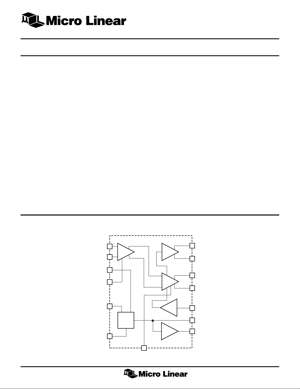
BLOCK DIAGRAM
ECLP
ECLN
VBIAS
TTL
V
CC
GND
PEAK
+
14
BUFFER
–
1
2
13
8
REF
4
9
I
OFF
PEAK
DRIVER
DRV
AMP
PTAT
7
6
RPK
LED
3
RTSET
5
11
DRV
VREF
10
PTAT
12
1
Page 2
ML4632
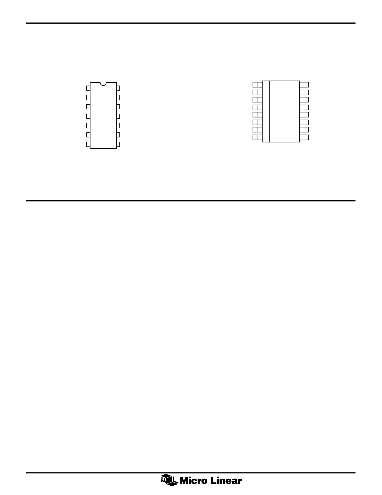
PIN CONFIGURATION
ML4632
14-Pin PDIP (P14)
ECLN
VBIAS
LED
GND
RTSET
RPK
PEAK
1
2
3
4
5
6
7
TOP VIEW
ECLP
14
TTL
13
PTAT
12
DRV
11
VREF
10
I
9
OFF
V
8
CC
PIN DESCRIPTION
NAME FUNCTION
ECLN Negative ECL data input. Tie to VBIAS for
single ended ECL operation or when ECLP is
used as an enable. Tie to ground during TTL
only operation.
VBIAS BIAS voltage for single ended ECL operation.
LED Fiber optic LED drive pin. Connect the LED
between this pin and VCC.
GND Negative power supply. The pin should be
tied to the grounded side of RTSET to improve
output accuracy and avoid a ground loop.
RTSET Output current programming pin. Connect a
resistor of value V
DRV/ILED
ground to set the high LED output current.
RPK Peaking circuit bias pin. Connect a resistor of
value V
DRV/IPEAK
from this pin to ground
when using the peaking circuit. Leave open
circuited when peaking is not used.
PEAK Peaking circuit output pin. When using
peaking, connect this pin to VCC through a
resistor of value RRPK. Then connect a
capacitor from this pin to the LED cathode.
When peaking is not used, open circuit RPK.
from this pin to
ML4632
16-Pin Wide SOIC (S16W)
ECLN
VBIAS
LED
GND
RTSET
RPK
PEAK
NC
NAME FUNCTION
V
I
OFF
CC
Positive power supply. +5 volts.
Connect a resistor from this pin to VCC to
1
2
3
4
5
6
7
8
TOP VIEW
ECLP
16
TTL
15
PTAT
14
DRV
13
VREF
12
I
11
10
9
V
NC
OFF
CC
increase the off current to the LED, i.e. 4.3KΩ
for 1mA. With this pin open, the default I
OFF
current is between 0.5–1.0mA.
VREF A constant 1.2V reference output used to set
up DRV.
DRV A DC input that sets the positive swing on
RTSET and the high level output current to
the LED.
PTAT Proportional to Absolute Temperature. A 1.0V
reference at 25°C that moves proportional to
absolute temperature, also used to set up
DRV. (See figure 1)
TTL TTL data input. Can also be used as an enable
during ECL operation. TTL = High (enabled),
TTL = Low (disabled).
ECLP Positive ECL data input controls signal to the
LED. Tie to VBIAS during TTL only operation
or use as an enable.
2
Page 3

ABSOLUTE MAXIMUM RATINGS
ML4632
Absolute maximum ratings are those values beyond which
the device could be permanently damaged. Absolute
maximum ratings are stress ratings only and functional
PEAK DC Output Current ..................................... 120mA
Storage Temperature .............................. –65°C to +150°C
Lead Temperature (Soldering 10 sec.) ..................... 260°C
device operation is not implied.
V
............................................................................... –0.3V to 6V
CC
Input Pin Voltages ............................. –0.3V to VCC +0.3V
LED Output Current ............................................. 120mA
ELECTRICAL CHARACTERISTICS
Over the recommended operating conditions of T
SYMBOL PARAMETER CONDITIONS MIN TYP MAX UNITS
I
CC
VREF VREF Voltage No Load 1.14 1.20 1.26 V
V
PTAT
V
I
LEDH
I
LEDL
t
t
PLH
t
PHL
t
PWD
V
V
PKTR
V
PKTF
I
ECL
I
TTL
V
I
OFF
VBIAS ECL BIAS Voltage VCC = 5V, T
Note 1: Limits are guaranteed by 100% testing, sampling or correlation with worst-case test conditions.
Note 2: Low Duty cycle pulse testing is performed at T
OS
R
t
F
PK
DO
Supply Current LED off 25 35 mA
PTAT Voltage No Load, T
Driver Offset VDRV = 1.2V, RTSET = 20Ω 50 mV
LED Current Accuracy VDRV = VREF, RTSET = 20Ω
High I
OFF
Low 0.5 0.7 1.0 mA
Rise Time VDRV = VREF, RTSET = 20Ω 4.5 ns
Fall Time VDRV = VREF, RTSET = 20Ω 4.5 ns
Propagation Delay VDRV = VREF, RTSET = 20Ω
Low to High TTL and ECL 10.0 ns
High to Low 10.0 ns
Pulse Width Distortion VDRV = VREF, RTSET = 20Ω 1.0 2.0 ns
Peaking Voltage R
Peaking Rise Time R
Peaking Fall Time R
ECL Input Current 20 µA
TTL Input Current 100 µA
Dropout Voltage between
pin 5 and 3 1.5 V
Additional LED Off Current VCC = 5V, R
.
A
= 0°C to 70°C, VCC = 5V ±5%, unless otherwise specified. (Note 1)
A
= 25°C 0.9 1.0 1.1 V
A
T
= 85°C 1.08 1.2 1.32 V
A
= open 54 60 66 mA
= 20Ω, C
RPK
= 20Ω, C
RPK
= 20Ω, C
RPK
= 100pF, R
PK
= 100pF, R
PK
= 100pF, R
PK
= 4.3KΩ 0.8 1.0 1.2 mA
IOFF
= 25°C 3.8 V
A
= 20Ω 1.08 1.2 1.32 V
PEAK
= 20Ω 4.5 ns
PEAK
= 20Ω 4.5 ns
PEAK
3
Page 4

ML4632
FUNCTIONAL DESCRIPTION
The ML4632 accepts ECL and TTL input signals and
generates a high speed, high accuracy output current
which is independent of supply voltage variations. The
output current is programmable from 20mA to 100mA.
A temperature coefficient can be programmed into the
output current and a peaking circuit can be added with
a few external components.
The input of the LED driver accepts both ECL and TTL
signals. The ECL input stage is a standard NPN differential
pair with a common mode range of between 3V and 4.5V
with a +5V supply. A bias voltage VBIAS is available for
biasing either ECL input for single-ended operation. The
TTL input has a standard switching range of between 0.8V
and 2.0V. These inputs are ANDed so that the extra input
can be used as an enable.
Output current to the LED is set by connecting the
appropriate resistance from RTSET to ground. With the
VREF and DRV pins tied together, the high level output
voltage at RTSET will be 1.2V. The current through the
LED. The output current with RTSET set to 20Ω will be
I
(HIGH) = 1.2V/R
LED
The low level output current is set internally by a resistor
at approximately 0.7mA. This current prebiases the LED
and results in faster optical rise times. The value of this
current can be increased by connecting a resistor from the
I
pin to VCC. The additional current will be equal to
OFF
(VCC – 0.7V)/R
IOFF
.
The voltage input at the DRV pin appears across the
RTSET pin when the LED is turned on. The current in
RTSET is directed through the LED. Therefore the voltage
set at DRV along with the RTSET resistor sets current
through the LED.
A temperature coefficient of between 0ppm/°C and
3300ppm/°C can be programmed into the high level
output current to compensate for the drop in LED optical
output power at high temperatures. This is accomplished
by driving the DRV pin from a resistor divider between the
VREF and PTAT pins.
When DRV is tied directly to PTAT, the peak voltage at
RTSET will be 1.0V at 25°C and have a 3300ppm/°C
temperature coefficient. At 85°C, PTAT is 1.2V and equal
to VREF. An arbitrary temperature coefficient less than
3300 ppm/°C can be set by using a resistor divider
between PTAT and VREF to set the voltage at DRV, as
shown in figure 1.
= 1.2V/20Ω = 60mA.
TSET
VREF
(10)
R1
DRV
REF
PTAT
PTAT
(12)
R2
(11)
DRV
AMP
TO
DRIVER
Figure 1. Current for Programming
Output Temperature Coefficient
In this configuration the temperature coefficient is
R
TC ppm C
I
LED HIGH
(/),
=°
3300
ILED
.
VV
+
102
=
()
RTSET
1
RR
12
R
RR
12
and
+
2
+
The output current will be a linear function of temperature.
A plot of I
versus temperature for several values of the
LED
programming resistance, R1 and R2, in figure 2.
60
55
(mA)
LED
I
50
45
R1 = 1Ω
R2 = 3R1
R1 = R2
R1 = 3R2
R2 = 0Ω
NOTE: R
025507585
T(°C)
Figure 2. I
LED
vs T, R
+ R
1
TSET
≥ 10kΩ
2
= 20Ω
4
Page 5

ML4632
The ML4632 output stage conducts full load current only
when the LED is on, and even then power dissipation in
the part is low because most of the +5V supply voltage is
dropped across the LED and external resistor R
TSET
. Even
with a low power design, the LED driver junction
temperature will rise above ambient due to quiescent
power dissipation and won’t exactly match the LED
junction temperature since it is also self-heating.
Therefore, the effectiveness of a temperature compensated
design will be related to component power dissipations,
thermal conductance of the PC board and packaging, and
the proximity of the LED driver to the LED.
The ML4632 also provides for peaking of the LED output
current. Peaking is used to counteract the effects of the
LED junction capacitance. By creating a controlled
overshoot and undershoot in the output current waveform,
charge is transferred to and from the LED capacitance on
the rising and falling edges of the output, speeding up rise
and fall times.
To provide peaking current, a second output stage is
biased up with a resistor from RPK to ground and another
from PEAK to VCC. When these bias resistors are set equal
to each other, a pulse will be generated across the R
PEAK
resistor with a magnitude equal to the voltage on the DVR
pin. A coupling capacitor transfers the rising and falling
edges of the output current waveform.
A typical application is shown in figure 3. When the
resistors R
RPK
and R
are both set to 20Ω, a pulse will
PEAK
be generated at the PEAK pin of magnitude 1.2V and
equivalent resistance 20Ω (assuming V
PEAK
PEAK
RPK
RPEAK
20Ω
RPK
20Ω
CPEAK
100pF
RTSET
20Ω
DRV
= 1.2V).
LED
DRIVER
RTSET
Figure 3. Application of the Peaking Circuit
The peaking current is coupled through the 100pF
capacitor, C
, which will transfer 120pC of charge to
PEAK
and from the LED on each cycle of output current. The
peaking circuit shown provides approximately a 70%
overshoot current into a 0Ω LED impedance. Peaking
currents will be slightly lower for real LED’s.
I
OUT
20Ω
20Ω
CPEAK
100pF
0.1µF
Note: The LED, PEAK and VCC traces should be very short and shielded with a
GND plane to reduce ringing and overshoot at the LED.
20Ω
TTL Driven Implementation
(No Temp. Comp)
ECLN
VBIAS
LED
GND
RTSET
RPK
PEAK
ECLP
TTL
PTAT
DRV
VREF
I
OFF
V
CC
I
OUT
I
OFF
4.7µF
= 60mA
= 0.7mA
TTL IN
+5V
5
Page 6

ML4632
6
Page 7

ML4632
Package: P14
14-Pin PDIP
0.740 - 0.760
(18.79 - 19.31)
14
0.070 MIN
(1.77 MIN)
(4 PLACES)
0.170 MAX
(4.32 MAX)
0.125 MIN
(3.18 MIN)
PIN 1 ID
1
0.050 - 0.065
(1.27 - 1.65)
0.016 - 0.022
(0.40 - 0.56)
0.100 BSC
(2.54 BSC)
SEATING PLANE
0.240 - 0.260
(6.09 - 6.61)
0.015 MIN
(0.38 MIN)
0.295 - 0.325
(7.49 - 8.25)
0º - 15º
0.008 - 0.012
(0.20 - 0.31)
7
Page 8

ML4632
Package: S16W
16-Pin Wide SOIC
0.400 - 0.414
16
(10.16 - 10.52)
0.024 - 0.034
(0.61 - 0.86)
(4 PLACES)
0.090 - 0.094
(2.28 - 2.39)
1
PIN 1 ID
0.050 BSC
(1.27 BSC)
0.012 - 0.020
(0.30 - 0.51)
0.291 - 0.301
(7.39 - 7.65)
0.095 - 0.107
(2.41 - 2.72)
SEATING PLANE
0.398 - 0.412
(10.11 - 10.47)
0.005 - 0.013
(0.13 - 0.33)
0º - 8º
0.022 - 0.042
(0.56 - 1.07)
0.009 - 0.013
(0.22 - 0.33)
ORDERING INFORMATION
PART NUMBER TEMPERATURE RANGE PACKAGE
ML4632CP 0°C to 70°C 14-Pin PDIP (P14)
ML4632CS 0°C to 70°C 16-Pin Wide SOIC (S16W)
© Micro Linear 1997 is a registered trademark of Micro Linear Corporation
Products described in this document may be covered by one or more of the following patents, U.S.: 4,897,611; 4,964,026; 5,027,116; 5,281,862; 5,283,483; 5,418,502; 5,508,570; 5,510,727; 5,523,940;
5,546,017; 5,559,470; 5,565,761; 5,592,128; 5,594,376; Japan: 2598946. Other patents are pending.
Micro Linear reserves the right to make changes to any product herein to improve reliability, function or design.
Micro Linear does not assume any liability arising out of the application or use of any product described herein,
neither does it convey any license under its patent right nor the rights of others. The circuits contained in this
data sheet are offered as possible applications only. Micro Linear makes no warranties or representations as to
whether the illustrated circuits infringe any intellectual property rights of others, and will accept no responsibility
or liability for use of any application herein. The customer is urged to consult with appropriate legal counsel
before deciding on a particular application.
8
2092 Concourse Drive
San Jose, CA 95131
Tel: 408/433-5200
Fax: 408/432-0295
DS4632-01
 Loading...