

Page 1
PRELIMINARY
ML4435 Sensorless BLDC Motor Controller
GENERAL DESCRIPTION
The ML4435 provides all the circuitry for sensorless
speed control of 3 phase Brushless DC Motors. Controller
functions include start-up circuitry, Back EMF commutation control, Pulse Width Modulation (PWM) speed control, pulse-by-pulse current limiting, motor coasting, and
under-voltage protection.
Motor starting is accomplished by commutating the motor
at a low frequency to produce low speed motion. The
low speed motion is used to generate a Back EMF signal.
A back EMF sampling circuit locks on to the motors position and controls commutation timing by forming a phase
locked loop (PLL). The commutation control circuitry also
outputs a speed feedback signal used in the speed control
loop. The speed control loop consists of an error amplifi er
and PWM comparator that produces a PWM duty cycle
for speed regulation. Motor current is limited by a pulseby-pulse PWM shutdown comparator that is tripped by
the voltage across an external current sense resistor. Commutation control, PWM speed control, and current limiting are combined to produce the output driver signals.
Six output drivers are used to provide gating signals to an
external 3 phase bridge power stage sized for the Brushless DC (BLDC) motor voltage and current requirements.
Additional functions include a motor coast function and
an under voltage lock out circuit to shut down the output
drivers in the event of a low voltage condition on the VCC
to the ML4435.
FEATURES
n Proprietary back-EMF sensing commutation technique
for motor communication without hall effect sensors
n PWM pulse-by-pulse current limiting to protect motor
and FET drivers
n Stand-alone operation; motor starts and stops with
power applied to the IC*
n Soft-start function limits start-up current
n PWM speed control for effi ciency and minimum FET
sizing
n Onboard under voltage lock out and power fail detect
n Tach output senses commutation of the motor
* Some External Components Required.
May, 2000PRELIMINARY DATASHEET
Page 2
PRELIMINARY
ML4435
WARRANTY
Micro Linear makes no representations or warranties with respect to the accuracy, utility, or completeness of the contents of
this publication and reserves the right to make changes to specifi cations and product descriptions at any time without notice.
No license, express or implied, by estoppel or otherwise, to any patents or other intellectual property rights is granted by this
document. The circuits contained in this document are offered as possible applications only. Particular uses or applications
may invalidate some of the specifi cations and/or product descriptions contained herein. The customer is urged to perform
its own engineering review before deciding on a particular application. Micro Linear assumes no liability whatsoever,
and disclaims any express or implied warranty, relating to sale and/or use of Micro Linear products including liability
or warranties relating to merchantability, fi tness for a particular purpose, or infringement of any intellectual property
right. Micro Linear products are not designed for use in medical, life saving, or life sustaining applications.
© Micro Linear 2000. is a registered trademark of Micro Linear Corporation. All other trademarks are
the property of their respective owners.
Products described herein may be covered by one or more of the following U.S. patents: 4,897,611; 4,964,026; 5,027,116;
5,281,862; 5,283,483; 5,418,502; 5,508,570; 5,510,727; 5,523,940; 5,546,017; 5,559,470; 5,565,761; 5,592,128; 5,594,376;
5,652,479; 5,661,427; 5,663,874; 5,672,959; 5,689,167; 5,714,897; 5,717,798; 5,742,151; 5,747,977; 5,754,012;
5,757,174; 5,767,653; 5,777,514; 5,793,168; 5,798,635; 5,804,950; 5,808,455; 5,811,999; 5,818,207; 5,818,669; 5,825,165;
5,825,223; 5,838,723; 5.844,378; 5,844,941. Japan: 2,598,946; 2,619,299; 2,704,176; 2,821,714. Other patents are pending.
PRELIMINARY DATASHEET
May, 20002
Page 3
BLOCK DIAGRAM
FB A
14
FB B
15
FB C
16
COMMUTATION
STATE MACHINE
R
3µs
SPEED SET
SPEED COMP
ISENSE
SOFT START
POWER ON
RESET PULSE
5
3
1
19
F
E
8.2 + 0.7V
2.2 + 0.7V
1V
225kΩ
225kΩ
NEUTRAL
5.8kΩ
2.9kΩ
TRIANGLE WAVE
SIMULATOR
A
B
C
D
LEVEL SHIFT
GENERATOR
CURRENT LIMIT
COMPARATOR
MUX
SPEED FB
–
+
COMP
–
PRELIMINARY
SIGN
CHANGER
6
+
0.7V
+
–
BACK
EMF SAMPLER
SPEED
ERROR AMP
+
–
PWM
COMPARATOR
+
–
5V
DQ
R
VREF + 0.7V
+
–
VOLTAGE
CONTROLLED
OSCILLATOR
GATING
LOGIC
AND
OUTPUT
DRIVERS
PULSE-BY-PULSE
CURRENT LIMIT
8.7V
+
–
+
LEVEL
0.97V
SHIFT
0.7V
COAST
UVLO COMPARATOR
COMP
–
1.5V
6V REFERENCE
+
COMP
–
0.9V
VREF
ML4435
18
SPEED FB
2
TACH
20
CVCO
RVCO
4
7
HA
8
HB
9
HC
11
LA
12
LB
13
LC
6
RT VCC GND
1710
ML4435 Block Diagram
May, 2000 PRELIMINARY DATASHEET 3
Page 4
PIN CONFIGURATION
PRELIMINARY
ML4435
20-P n PDIP P20
20-P n SOIC S20
ISENSE
TACH
SPEED COMP
RVCO
SPEED SET
RT
HA
HB
HC
VCC
2
3
4
5
6
9
0
TOP VIEW
20
9
6
5
4
3
2
CVCO
SOFT START
SPEED FB
ND
FB C
FB B
FB A
LC
LB
LA
ML4435
PIN DESCRIPTIONS
PIN NAME FUNCTION
1 ISENSE Motor current sense input which triggers pulse by pulse current limit when
ISENSE exceeds 0.55V
2 TACH A clock output of 6 pulses per commutation cycle when SPEED FB is greater
than 0.97V otherwise the TACH output is at 5V
3 SPEED COMP Connection node for speed loop compensation components
4 RVCO Connection node for external resistor to set VCO frequency
5 SPEED SET DC input for setting motor speed
6 RT External resistor from this pin to ground controls the IC's PWM timing (frequency)
7 HA High-side output driver for motor phase A
8 HB High-side output driver for motor phase B
9 HC High-side output driver for motor phase C
10 VCC Power Supply input
11 LA Low-side output driver signal for motor phase A
12 LB Low-side output driver signal for motor phase B
13 LB Low-side output driver signal for motor phase C
14 FB A Back EMF signal input for motor phase A
15 FB B Back EMF signal input for motor phase B
16 FB C Back EMF signal input for motor phase C
17 GND Signal and power ground
18 SPEED FB Connection node for back-EMF sensing compensation components
19 SOFT START Connection node for external soft start capacitor which reduces start up current
20 CVCO Connection node for external capacitor to set VCO frequency. Forcing this input
below 1.5V causes the commutation to stop and the motor to coast
PRELIMINARY DATASHEET
May, 20004
Page 5
PRELIMINARY
FUNCTIONAL DESCRIPTION
ML4435
COMPONENT SELECTION
Selecting external components for the ML4435 requires
calculations based on the motor’s electrical and mechanical parameters. The following is a list of the motor parameters needed to for these calculations:
The maximum DC motor supply voltage V MOTOR (V)
The maximum operating current I MAX (A)
The winding resistance measured line to line Rl-l Ω
The number of magnetic poles N (Unitless)
The Back EMF constant Ke (V s/RAD)
The torque constant Kτ (N m/A) of the motor (Kτ = Ke
in SI units)
The maximum speed of operation RPMMAX (RPM)
The moment of inertia J (Kg m2 ) of the motor and its
load
The viscous damping factor ζ (Unitless) of the motor and
its load
If one or more of the above values is not known, it is
still possible to pick components for the ML4435, but
some experimentation may be necessary to determine the
optimal values. All quantities are in SI units unless otherwise specifi ed. The following formulas and component
selection graphs should be considered as a starting point
from which to optimize the application. All calculations
for capacitors and resistors should be used as the fi rst
approximation for selecting the closest standard value.
SUPPLY VOLTAGE AND ON-CHIP VOLTAGE
REFERENCE
OUTPUT DRIVERS
The output drivers LA, LB, LC, HA, HB, and HC provide
totem pole output drive signals for a 3 phase bridge power
stage. All control functions in the ML4435 translate to
outputs at these pins. LA, LB, LC provide the low side drive
signals for phases A, B, and C of the 3 phase power stage
and are 12V active high signals. HA, HB, and HC provide
the high side signals for phases A, B, and C of the 3 phase
power stage and are 12V active low signals.
CURRENT LIMITING IN THE 3 PHASE BRIDGE
POWER STAGE
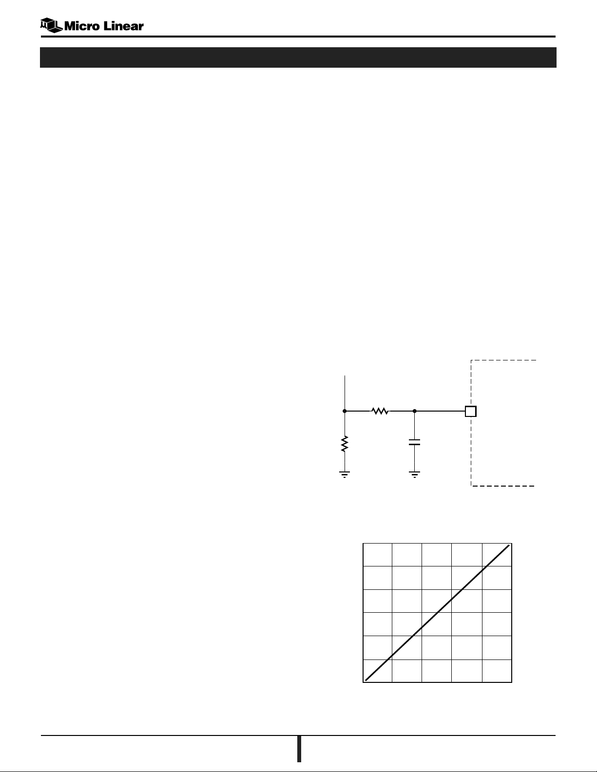
A current sense resistor RSENSE shown in Figure 1 is
installed in the 3 phase power stage to regulate the maximum current in the power stage and the BLDC motor.
Current regulation is accomplished by shutting off the
output drivers LA, LB, and LC for the remainder of the
PWM period if the voltage across RSENSE exceeds the
current limit threshold set by the SOFT START (pin 19).
The maximum power dissipated in RSENSE is shown in
Figure 2.
RSENSE
R
C
ISENSE
VCC
The supply voltage at VCC (pin 10) is nominally
12V ± 10%. A bypass capacitor of 0.1µF to ground as
close as possible to VCC (pin 10) is recommended.
RT
An internal 6V reference is generated inside the ML4435.
The reference appears on RT (pin 6). A resistor to ground
on RT sets the PWM frequency. This resistor can be
replace with a potentiomenter for use in setting the speed
command. This topic is discussed under the PWM SPEED
CONTROL section. Note: Buffer this pin with an op amp
with at least a 1MΩ input impedance if external circuits
are necessary.
May, 2000 PRELIMINARY DATASHEET 5
Figure 1. Current Limit with RSENSE
6
5
4
3
RSENSE Po er Rat n W
2
0
02
Figure 2. RSENSE Power vs. Motor Current
4
IMAX [MOTOR] A
60
Page 6

PRELIMINARY
FUNCTIONAL DESCRIPTION
ML4435
SOFT START
The voltage at SOFT START (pin 19) sets the current limit
threshold. The ML4435 has an internal voltage divider
with a 1.1V supply voltage. This circuit is shown in Figure
3. The divider consists of two 225k Ω resistors setting
the current limit threshold to approximately 0.55V. An
external voltage divider off of VCC or an external reference
can be used to override the default setting of SOFT START
by using a divider with 10 times the current draw of the
internal divider.
.V
225kΩ
CSOFT START
SOFT START
9
0.5V
225kΩ
RSENSE
The function of RSENSE is to provide a voltage proportional to the motor current, for current limiting. The default
trip voltage across RSENSE is 0.6V as set by the SOFT
START (pin 19). The current sense resistor should be a
low inductance resistor such as a carbon composition. For
resistors in the milli ohms range wire wound resistors tend
to have low values of inductance. RSENSE can be selected
using Figure 4. The power rating of RSENSE should be
sized to handle the power dissipation (I MAX squared
times RSENSE) seen at maximum current.
ISENSE FILTER
An RC lowpass fi lter is required at the ISENSE input pin
to remove the voltage spike on the leading edge of the
current sense signal caused by the diode reverse recovery
shoot through current. Absent the fi lter, false triggering of
the current limit could occur.
The recommended starting values for this circuit are
R = 1KΩ and C = 1000pF a confi guration that will fi lter
out spikes less than 1µs long. It is recommended that the
capacitor value not be increased beyond 330pF.
Figure 3. SOFT START Function
A capacitor to ground on the SOFT START pin can be used
to provide a soft ramping of the current limit on power up.
The ramp time can be selected using Figure 4.
30
RAMP TIME s
5
0
050
C SOFT START F
00
Pulse-By-Pulse Current Limiting
When current limit is activated by the voltage on ISENSE
exceeding the voltage on SOFT START the current limit is
tripped, turning off LA, LB, and LC for the remainder of
the PWM period.
COMMUTATION CONTROL
A 3 phase Brushless DC motor requires electronic com-
BEFORE FILTERIN
AFTER FILTERIN
Figure 4. SOFT START Ramp Time vs. CSOFTSTART
PRELIMINARY DATASHEET
Figure 5. ISENSE Filter Wave Forms
May, 20006
Page 7

PRELIMINARY
FUNCTIONAL DESCRIPTION
ML4435
mutation to achieve rotational motion. Electronic commutation requires the switching on and off of the power
switches of a 3 phase half bridge. For torque production
to be achieved in one direction the commutation is dictated by the rotor’s position. Electronic commutation in
the ML4435 is achieved by turning on and off, in the
proper sequence, one L output from one phase and one H
output from another phase. There are six combinations of
L and H outputs (six switching states) that constitute a full
commutation cycle as illustrated in Table 1 labeled state
A through F. This switching sequence is programmed into
the commutation state machine as illustrated in Figure 6.
Clocking of the commutation state machine is provided by
the output of a VCO.
VOLTAGE CONTROLLED OSCILLATOR
The VCO outputs a TTL compatible clock on the TACH
OUTPUT DRIVERS
LA LB LC HA HB HC
LOW LOW HI H LOW HI H HI H
A
(pin 2) proportional to the input voltage to the voltage
controlled oscillator SPEED FB (pin 18). The proportion of
frequency to voltage or VCO constant Kv is set by a resistor
to ground on RVCO (pin 4) and capacitor to ground on
CVCO (pin 20) as shown in Figure 7. RVCO sets up a
current proportional to the VCO input voltage SPEED FB
minus 0.7V. This current is used to charge and discharge
CVCO between the threshold voltages of 2V and 3.75V as
shown in Figure 7. RVCO has a lower voltage limit of 0.2V.
The resulting triangle wave of CVCO corresponds to the
clock on the TACH pin, this is also illustrated in Figure 7. Kv
should be set so that the VCO output frequency corresponds
to the maximum commutation frequency FMAX and thus the
maximum motor speed when the VCO input is equal to or
slightly less than 6V. CVCO and RVCO can be selected by
fi rst calculating FMAX and then using the selection graph in
Figure 8. FMAX is calculated as follows:
FMAX = 0.05 x RPMMAX x N
Where: RPMMAX = The maximum speed of operation
(RPM). N = The number of magnetic poles (Unitless).
TACH
B
LOW LOW HI H HI H LOW HI H
C
STATE
Table 1. Communication Control States
POWER ON
RESET PULSE
HI H LOW LOW HI H LOW HI H
D
HI H LOW LOW HI H HI H LOW
E
LOW HI H LOW HI H HI H LOW
F
LOW
HI H LOW LOW HI H HI H
COMMUTATION
STATE MACHINE
R
3s
A
F
B
= DRIVER ON
CLK VCO
The TACH (pin 2) outputs the VCO frequency. This is 6
SPEED FB
LEVEL
SHIFT
0. V
+
CVCO
20
RVCO
4
VOLTA E
CONTROLLED
OSCILLATOR
3. 5V
2V
0.9V
E
Figure 6. Commutation State Machine
C
D
Figure 7. VCO Control
May, 2000 PRELIMINARY DATASHEET 7
Page 8

PRELIMINARY
FUNCTIONAL DESCRIPTION
ML4435
times the commutation frequency. The TACH out also
indicates a low motor speed by staying TTL high when the
motor is at its minimum speed (SPEED FB below 0.97V).
BACK EMF SAMPLER
The input to the VCO (pin 18) SPEED FB is controlled by
the Back EMF Sampler. The back EMF sense pins FB A,
FB B, and FB C inputs to the back EMF sampler require
a signal from the motor phase leads that is below the
VCC of the ML4435. The phase sense input impedance is
8.7kΩ. If the motor voltage is greater than the VCC of the
ML4435 then this requires a series resistor RFB from the
motor phase lead shown in Figure 8. RFB can be selected
by using the graph in Figure 9 or using the following
equation:
RFB = 8.7k (
VMOTOR
12
-1)W
BLDC
MOTOR
The back EMF sampler takes the motor phase voltages
divided down to signals that are less than VCC (12V
nominal) and calculates the neutral point of the motor by
the following equation:
VNEUTRAL = (FB A + FB B + FB C)/3
This allows the ML4435 to compare the back EMF signal
to the motors neutral point without the need for bringing
out an extra wire on a WYE wound motor. For DELTA
wound motors there isn’t a physical neutral to bring out so
this reference point must be calculated anyway.
The back EMF sampler takes the motor phase that is not
driven (i.e. if LA and HB are on then phase A is driven
low and phase B is driven high then phase C is sampled).
The sampled phase provides a back EMF signal that is
compared against the neutral of the motor. The sampler
is controlled by the commutation state machine. The
sampled back EMF is compared to the neutral through an
error amplifi er. The output of the error amplifi er outputs
a charging or discharging current to SPEED FB (pin 18)
which provides the voltage to the VCO.
RFBA
RFBB
RFBC
ABC
Figure 8. Back EMF Sampler Confi guration
2,000
0,000
,000
6,000
R B F A, B, C Ω
4,000
2,000
FBA
4
FBB
5
6
FBC
BACK EMF SENSING PHASE LOCKED LOOP
COMMUTATION CONTROL
The three blocks: The commutation state machine, the
VCO, and the back EMF sampler form a phase locked
loop that locks the commutation clock onto the back EMF
signal. The complete phase locked loop is illustrated in
Figure 10. The phased locked loop requires a lead lag
fi lter that is set by external components on SPEED FB (pin
18). The fi lter components in Figure 10 work for most
applications. If performance is unstable C1 and C2 can
go up or down a decade in value as low as the C2 stays
equal to C1 x 10.
FBA
4
FBB
5
FBC
6
BACK EMF
SAMPLER
COMMUTATION
STATE MACHINE
VCO
SPEED FB
CSFB
RSFB
CSFB2
RSFB2
0
05
Motor Volta e [Max] V
Figure 9. RFB vs. VMOTOR [MAX]
25 30
20
PRELIMINARY DATASHEET
Figure 10. Phase Locked Loop
May, 20008
Page 9

PRELIMINARY
FUNCTIONAL DESCRIPTION
ML4435
MOTOR START-UP
When power is fi rst applied to the ML4435, the motor is at
rest and thus, the back EMF is equal to zero. The motor
needs to be rotating for the Back EMF sampler to lock onto
the rotor position and commutate the motor. The ML4435
uses a minimum VCO frequency to begin commutating the
motor. This low frequency commutation is set by the 0.2V
clamp on RVCO, this provides a commutation frequency
at 1/30th of the maximum frequency.
RUN MODE
After the Back EMF sensing PLL has locked on to the
motor’s position, the motor is running in closed loop control. At this point, the speed control loop should force the
motor speed to the speed that corresponds to the SPEED
SET voltage.
PWM SPEED CONTROL
Speed control is accomplished by setting a speed command at SPEED SET (pin 5) with an input voltage from 0.2
to 6V. The accuracy of the speed command is determined
by the external components RVCO and CVCO. There are
a number of methods to control the speed command on
the ML4435. One method is to use a potentiometer from
RT to ground with the wiper going to SPEED SET. If SPEED
SET is controlled from a microcontroller, a DAC that uses
RT as its input reference can be used. The RT voltage must
be buffered connecting it to external circuits. The speed
command is compared with the sensed speed from SPEED
FB minus 0.7V (pin 18) through a transconductance error
amplifi er. The output of the speed error amplifi er is SPEED
COMP (pin 3). SPEED COMP is clamped between 8.2V
and 2.2V. A signal of 8.2V corresponds to full PWM duty
cycle and 2.2V corresponds to 0% duty cycle. Speed
loop compensation components are placed on this pin as
shown in Figure 11.
The voltage on SPEED COMP (pin 3) is compared with a
triangle wave oscillator to create a PWM duty cycle. The
PWM oscillator creates a triangle wave function from 3V
to 7V as shown in Figure 11. The frequency of the triangle
wave oscillator is set by a resistor to ground on RT (pin 6).
RT can be selected from the graph in Figure 12.
The PWM duty cycle from the speed control loop is gated
the pulse-by-pulse current limit that controls the LA, LB,
and LC output drivers.
SPEED FB
SPEED
WAVE
ERROR AMP
–
+
V
3V
PWM
COMPARATOR
+
–
SPEED
SET
5
–
+
LEVEL SHIFT
0. V
.2 - 0. V
SPEED
COMP
3
CSE
2.2 + 0. V
TRIAN LE
COMPARATOR
Figure 11. PWM Oscillator Circuit
000
The speed loop compensation components are calculated
as follows:
C
SC
Rsc
144
2
=
=
22π
NxKexVMOTOR R C
×××
.
2
J RI freq
××××
π
VCO VCO
2
10
freq Csc
×× ×
Csc1 = 10 x Csc2
Where freq is the speed loop bandwidth in Hz.
May, 2000 PRELIMINARY DATASHEET 9
RT kΩ
00
0
PWM FRE UENCY kHz
Figure 12. RT vs PWM Frequency
000
Page 10

PRELIMINARY
FUNCTIONAL DESCRIPTION
ML4435
COAST
When CVCO (pin 20) is pulled below 1.5V the output
drivers LA, LB, LC and HA, HB, and HC are turned off.
The COAST function shuts all power off from the motor
allowing it to coast to a stop. The COAST function in (pin
20) is confi gured as shown in Figure 13 and can be driven
by a switch to ground or open collector to ground also
shown in Figure 13.
3. 5V
2V
+
COMP
.5V
–
Figure 13. Coast Control
CVCO
20
COAST
UNDER VOLTAGE PROTECTION
Undervoltage protection is used to protect the 3 phase
bridge power stage from a low VCC condition. Undervoltage is triggered at VCC of 9.2V or under. Undervoltage
also turns off all output drivers LA, LB, LC, HA, HB, and
HC. The comparator that triggers undervoltage protection
has 500mV of hystersis.
INTERFACING THE OUTPUT DRIVERS TO THE 3
PHASE BRIDGE POWER STAGE
The most fl exible confi guration is to use high side drivers
to control N-Channel MOSFETs (or IGBTs) allowing applications from less than 12V up to 170V. Figure 14a shows
the ML4435 and all the support circuitry in a typical
application. Figure 14b shows a power stage using the
IR2118 high side drivers from International Rectifi er and
high voltage MOSFETs.
P
N.C.
2
N.C.
3
4
5
6
TP 3 TACH
C4
TP SPEED SET
C3 2200 F
C5
0.33 F
0F
R6 0k
R k
R4 20k
TP 0 ISENSE
R2 00k
R 90.9k
R3 k
2V
0. F
9
0
2
3
4
5
6
RUN
SW
N.C.
R 0 k
R5
0k
C
.F
C9
.0 F
SW4PDT
COAST
R6
200k
N.C.
N.C.
TP 2
S FB
TP 5 LIMIT
ML4435
ISENSE
2
TACH
3
S COMP
4
RVCO
5
S SET
6
RT
HA
HB
9
HC
0
VCC
C2
C
4F
CVCO
I LIMIT
FB C
FB B
FB A
S FB
20
9
ND
6
5
4
3
2
R k
R9 k
R 2 k
LC
LB
LA
C0
00 F
C
.033 F
2V
9
20
N.C.
2
22
N.C.
23
24
N.C.
25
26
N.C.
IDC 26
Figure 14a. ML4435 Typical Application
PRELIMINARY DATASHEET
May, 200010
Page 11

PRELIMINARY
FUNCTIONAL DESCRIPTION
.5k
PHASE C
TERMINAL
PHASE B
PHASE A TERMINAL
SB
TERMINAL
SA
R44
SC
4
IRF644
5
IRF644
R3
3
IRF644
R32
.5k
.5k
R43 .0k
R3 .0k
6
2
IRF644
IRF644
R49
ML4435
0k
R4
0k
R42
D3 UF4005
W
0.4 Ω
R4
R36
D2 UF4005
R35
F
C6
6
5
U3
2
3
4
IR2
F
C5
0k
0k
F
C4
6
5
U2
2
3
4
IR2
F
C3
0k
2N440
2N440
9
2N4403
F
C9
2N4403
02
F
C
IRF644
F SA FUSE
2
HV
ND
P2
2PIN
P
2
C4
C0
R3 .0k
0.33 F
250V
0.33 F
250V
C3
200V
390 F
R50 0
C2
2V
ND
ND
ISENSE
0
2
3
3
4
5
HA
6
SA
LA
ND
HB
9
SB
LB
HC
ND
4
SC
LC
R30
D UF4005
UNUSED
5
ND
ISENSE
0k
U
ND
6
ND2VND
F
C2
6
2
3
F
C
HA
9
2022223242526
ND
ND
2N440
5
4
IR2
LA
LC
LB
ND
IDC 26
ND
HB
HC
2N4403
F
C
ND
Figure 14b. Power Stage
May, 2000 PRELIMINARY DATASHEET 11
Page 12

PRELIMINARY
ML4435
ELECTRICAL TABLES
Unless otherwise specifi ed, Ta= Operating Temperature Range, VCC= 12V +/- 10%, RT= 50k
SYMBOL PARAMETER CONDITIONS MIN TYP MAX UNITS
REFERENCE
RT 5.8 6 6.2 V
VCO
2
RVCO Lower Range
Upper Range
CVCO Lower Threshold
Upper Threshold
Coast Enable Threshold
Back EMF Blanking Threshold
SPEED FEEDBACK
Output Range
V Minimum Frequency
TACH Out Disabled Threshold
I Back EMF Sampler
BACK EMF SENSING
Feed Back Input Range
TACH
TACH Out Low ISINK = 100µA 0.2 0.4 V
TACH Out High ISOURCE =100µA 4.3 4.8 V
SPEED ERROR AMP
SPEED SET Range
I SPEED COMP V SPEED COMP = 5.1V +/-45 µA
SPEED COMP Output Lower Clamp
SPEED COMP Output Upper Clamp
OSCILLATOR
PWM Frequency N1, N2, N3 17 25 33 kHz
Duty Cycle
CURRENT SENSE
V SOFT START 0.48 0.58 0.68 V
ISENSE Threshold
OUTPUTS (N1, N2, N3, P1, P2, AND P3)
Output Low ISINK = 20mA 0 0.5 1 V
Output High (VCC-VOUT) ISOURCE = 20mA 0 0.5 1 V
UNDER-VOLTAGE LOCKOUT
Start Threshold 8.7 9.2 9.7 V
Under Voltage Threshold 8.2 8.7 9.2 V
SUPPLY
ICC Supply Current 15 mA
0.2 V
2
2
2 V
2
3.75 V
2
1.5 V
2
2.875 V
2
0 6.7 V
2
V Speed Feedback 0.9 V
2
TACH Out = Hi 0.97 V
2
V Speed Feedback = 3.3V +/-80 µA
2
FB A, FB B, and FB C 0 VCC V
2
0 6 V
2
I = ±45µA 2.15 V
2
I = ±45µA 8.2 V
2
N1, N2, N3 0 100 %
2
0.58 V
6
V
Note 1: Limits are guaranteed by 100% testing, sampling, or correlation with worst case test conditions
Note 2 Guaranteed by design, not tested
PRELIMINARY DATASHEET
May, 200012
Page 13

PRELIMINARY
ML4435
PHYSICAL DIMENSIONS
20
PIN ID
0.060 MIN
.52 MIN
4 PLACES
0. 0 MAX
4.32 MAX
0. 25 MIN
3. MIN
(inches/millimeters)
Packa e P20
20-P n PDIP
.0 0 - .035
25.65 - 26.29
0.055 - 0.065
.40 - .65
0.0 6 - 0.022
0.40 - 0.56
0. 00 BSC
2.54 BSC
0.240 - 0.260
SEATIN PLANE
6.09 - 6.6
0.0 5 MIN
0.3 MIN
0.295 - 0.325
.49 - .26
0º - 5º
0.00 - 0.0 2
0.20 - 0.3
0.024 - 0.034
0.6 - 0. 6
4 PLACES
0.090 - 0.094
2.2 - 2.39
Packa e S20
20-P n SOIC
0.49 - 0.5 2
PIN ID
2.65 - 3.00
0.050 BSC
.2 BSC
0.0 2 - 0.020
0.30 - 0.5
0.29 - 0.30
0.095 - 0. 0
2.4 - 2. 2
SEATIN PLANE
.39 - .65
0.005 - 0.0 3
0. 3 - 0.33
0.39 - 0.4 2
0. - 0.4
0º - º
0.022 - 0.042
0.56 - .0
0.00 - 0.0 5
0. - 0.3
20
May, 2000 PRELIMINARY DATASHEET 13
Page 14

PRELIMINARY
ORDERING INFORMATION
PART NUMBER TEMPERATURE RANGE PACKAGE
ML4435CP 0ºC to 70ºC 20 Pin PDIP (P20)
ML4435CS 0ºC to 70ºC 20 Pin SOIC (S20)
ML4435IP -40ºC to 85ºC 20 Pin PDIP (P20)
ML4435IS -40ºC to 85ºC 20 Pin SOIC (S20)
ML4435
Micro Linear Corporation
2092 Concourse Drive
San Jose, CA 95131
Tel: (408) 433-5200
Fax: (408) 432-0295
www.microlinear.com
PRELIMINARY DATASHEET
DS4435-01
May, 200014
 Loading...