

Page 1
www.fairchildsemi.com
ML4425
Sensorless BLDC Motor Controller
Features
• Stand-alone operation
• Motor starts and stops with power to IC
• On-board start sequence: Align ♦ Ramp ♦ Set Speed
• Patented Back-EMF commutation technique provides
jitterless torque for minimum “spin-up” time
• Onboard speed control loop
• PLL used for commutation provides noise immunity from
PWM spikes, compared to noise sensitive zero crossing
technique
• PWM control for maximum efficiency
• Direct FET drive for 12V motors; drives high voltage
motors with IC buffers
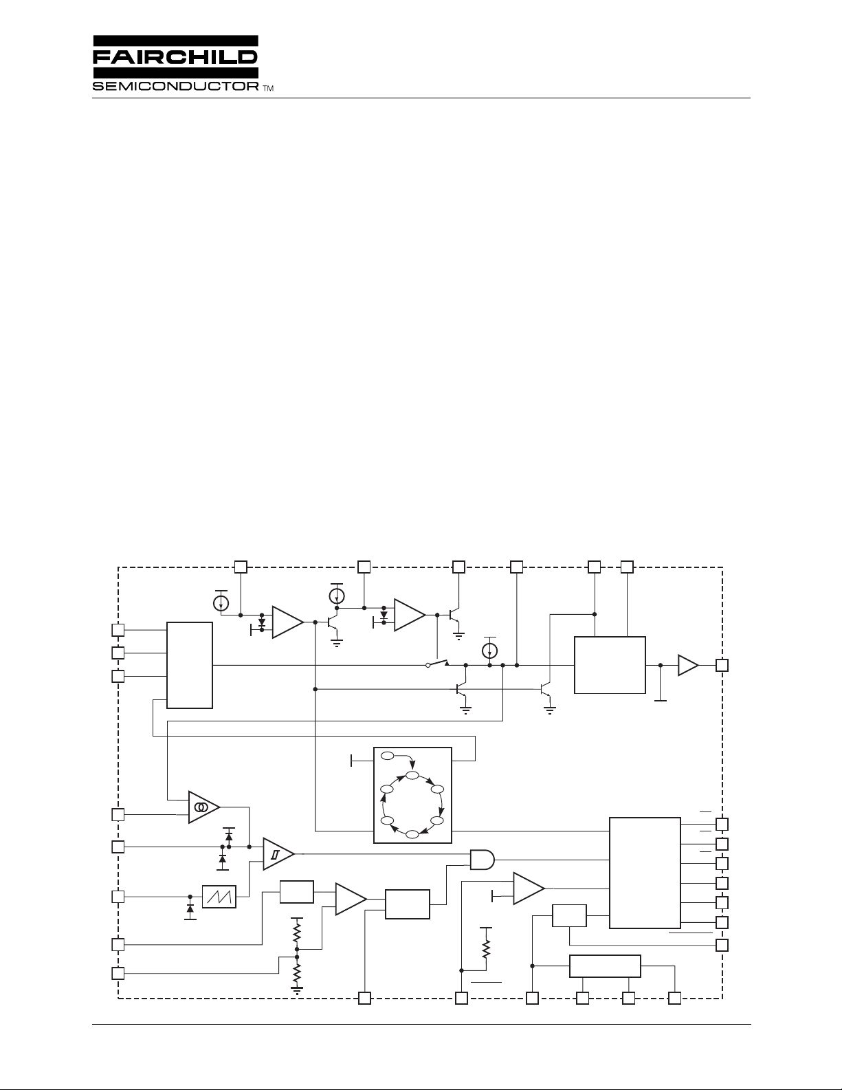
Block Diagram
17
C
DD
1.5V
AT
750nA
–
+
V
750nA
FB A
22
FB B
23
FB C
24
BACK
EMF
SAMPLER
19
V
DD
C
RT
–
1.5V
+
General Description
The ML4425 PWM motor controller provides all of the
functions necessary for starting and controlling the speed of
delta or wye wound Brushless DC (BLDC) motors without
Hall Effect sensors. Back EMF voltage is sensed from the
motor windings to determine the proper commutation phase
sequence using a PLL. This patented sensing technique will
commutate a wide range of 3-Phase BLDC motors and is
insensitive to PWM noise and motor snubbing circuitry.
The ML4425 limits the motor current using a constant offtime PWM control loop. The velocity loop is controlled with
an onboard amplifier. The ML4425 has circuitry to ensure
that there is no shoot-through in directly driven external
power MOSFETs.
The timing of the start-up sequence is determined by the
selection of three timing capacitors. This allows optimization
for a wide range of motors and loads.
21
C
500nA
RR
20
SPEED
FB
V
DD
15 16
C
VCO
VOLTAGE
CONTROLLED
OSCILLATOR
R
VCO
VCO/TACH
13
8
SPEED SET
5
SPEED COMP
C
T
6
I
SENSE
1
I
LIMIT
12
1.7V
VCO
OUT
VCO
OUT
+
–
3.9V
–
+
1.7V
–
+
8kΩ
20kHz
16kΩ
V
× 5
REF
R
A
I
LIMIT
B
COMMUTATION
STATE MACHINE
C
D
GATING
LOGIC
&
OUTPUT
DRIVERS
REF
25
1.4V
V
DD
BRAKE
4kΩ
–
+
UVLO
REFERENCE
V
DD
14
GND27R
28
HA
HB
HC
LA
LB
LC
UV FAULT
V
REF
7
2
3
4
9
10
11
18
F
E
1-SHOT
C
IOS
26
REV. 1.0.2 7/2/01
Page 2
ML4425 PRODUCT SPECIFICATION
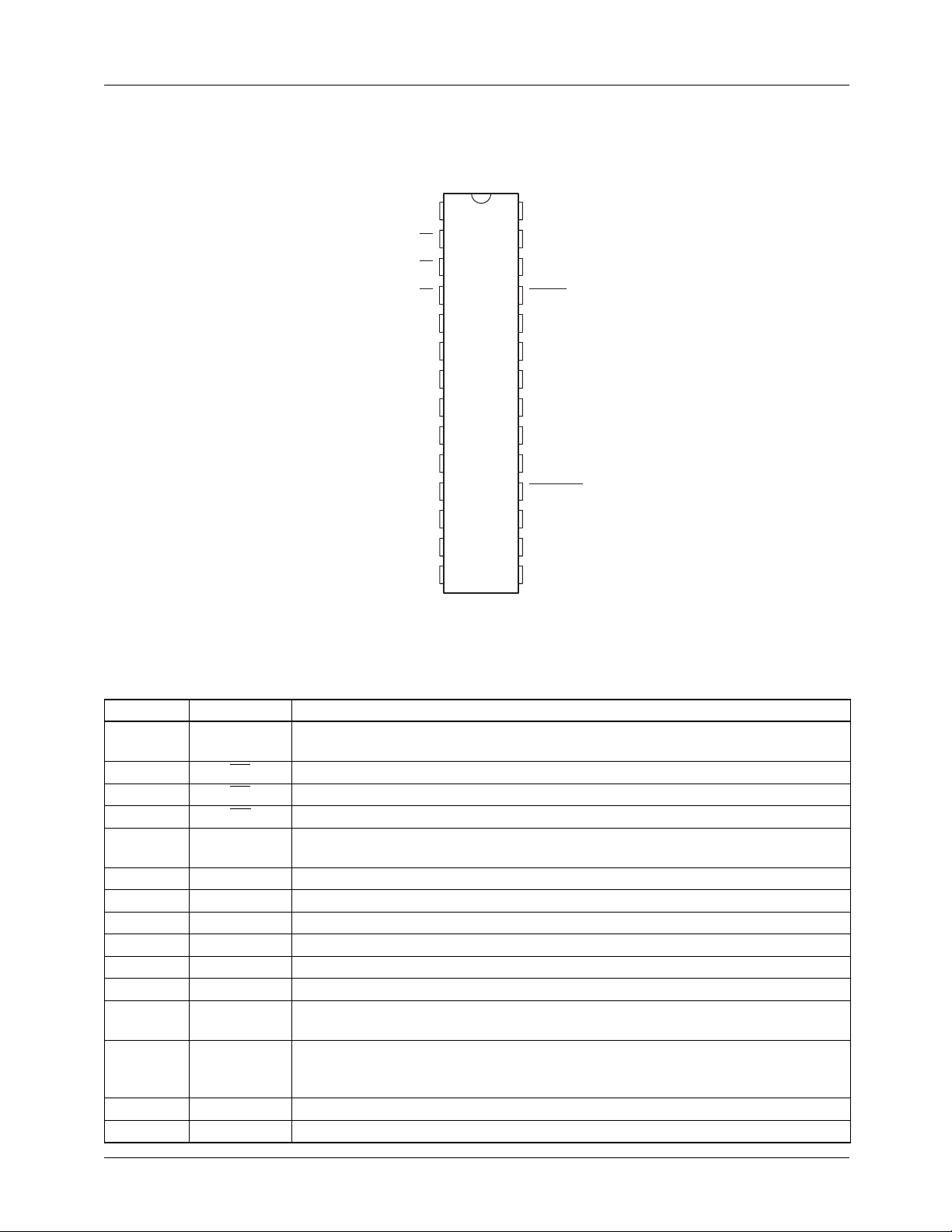
Pin Configuration
28-Pin Narrow PDIP (P28N)
I
SENSE
SPEED COMP
V
SPEED SET
I
LIMIT
VCO/TACH
ML4425
28-Pin SOIC (S28)
1
HA
2
HB
3
HC
4
5
C
6
T
7
REF
8
LA
9
LB
10
LC
11
12
13
V
14
DD
TOP VIEW
GND
28
R
27
REF
C
26
IOS
BRAKE
25
FB C
24
FB B
23
FB A
22
C
21
RR
SPEED FB
20
C
19
RT
UV FAULT
18
C
17
AT
R
16
VCO
C
15
VCO
Pin Description
Pin Name Function
1I
SENSE
2HA
3HBActive low output driver for the phase B high-side switch.
4HCActive low output driver for the phase C high-side switch.
5 SPEED
COMP
6C
V
T
REF
8 SPEED SET Speed loop input which ranges from 0 (stopped) to V
9 LA Active high output driver for the phase A low-side switch.
10 LB Active high output driver for the phase B low-side switch.
11 LC Active high output driver for the phase C low-side switch.
12 I
LIMIT
13 VCO/TACH This TTL level output corresponds to the signal used to clock the commutation state
14 V
15 C
DD
VCO
Motor current sense input. When I
LB, and LC are shut off for a fixed time determined by C
exceeds 0.2 ↔ I
SENSE
the output drivers LA,
LIMIT,
.
IOS
Active low output driver for the phase A high-side switch.
Speed control loop compensation is set by a series resistor and capacitor from
SPEED COMP to GND.
A capacitor from C
to GND sets the PWM oscillator frequency.
T
6.9V reference voltage output.
(maximum speed).
REF
Voltage on this pin sets the I
threshold voltage at 0.2 ↔ I
SENSE
, leaving this pin
LIMIT
unconnected selects an internally set threshold.
machine. The output frequency is proportional to the motor speed when the backEMF sensing loop is locked onto the rotor position.
12V power supply input.
A capacitor to GND sets the voltage-to-frequency ratio of the VCO.
2
REV. 1.0.2 7/2/01
Page 3
)
PRODUCT SPECIFICATION ML4425
Pin Description
(continued)
Pin Name Function
16 R
17 C
18 UV
FAULT This output goes low when V
VCO
AT
An resistor to GND sets up a current proportional to the input voltage of the VCO.
A capacitor to GND sets the time that the controller stays in the align mode.
drops below the UVLO threshold, and indicates that
DD
all output drivers have been disabled.
19 C
RT
A capacitor to GND sets the time that the controller stays in the ramp mode.
20 SPEED FB Output of the back-EMF sampling circuit and input to the VCO. An RC network
connected to SPEED FB sets the compensation for the PLL loop formed by the
back-EMF sampling circuit, the VCO, and the commutation state machine.
21 C
RR
A capacitor to between C
and SPEED FB sets the ramp rate (acceleration) of the
RR
motor when the controller is in ramp mode.
22 FB A The motor feedback voltage from phase A is monitored through a resistor divider for
back-EMF sensing at this pin.
23 FB B The motor feedback voltage from phase B is monitored through a resistor divider for
back-EMF sensing at this pin.
24 FB C The motor feedback voltage from phase C is monitored through a resistor divider for
back-EMF sensing at this pin.
25 BRAKE A logic low input activates motor braking by shutting off the high-side output drivers
and turning on the low-side output drivers.
26 C
27 R
IOS
REF
A capacitor to GND sets the time that the low-side output drivers remain off after
I
exceeds its threshold .
SENSE
An 137k Ω resistor to GND sets a current proportional to V
that is used to set all
REF
the internal bias currents except for the VCO.
28 GND Signal and power ground.
Absolute Maximum Ratings
Absolute maximum ratings are those values beyond which the device could be permanently damaged. Absolute maximum
ratings are stress ratings only and functional device operation is not implied.
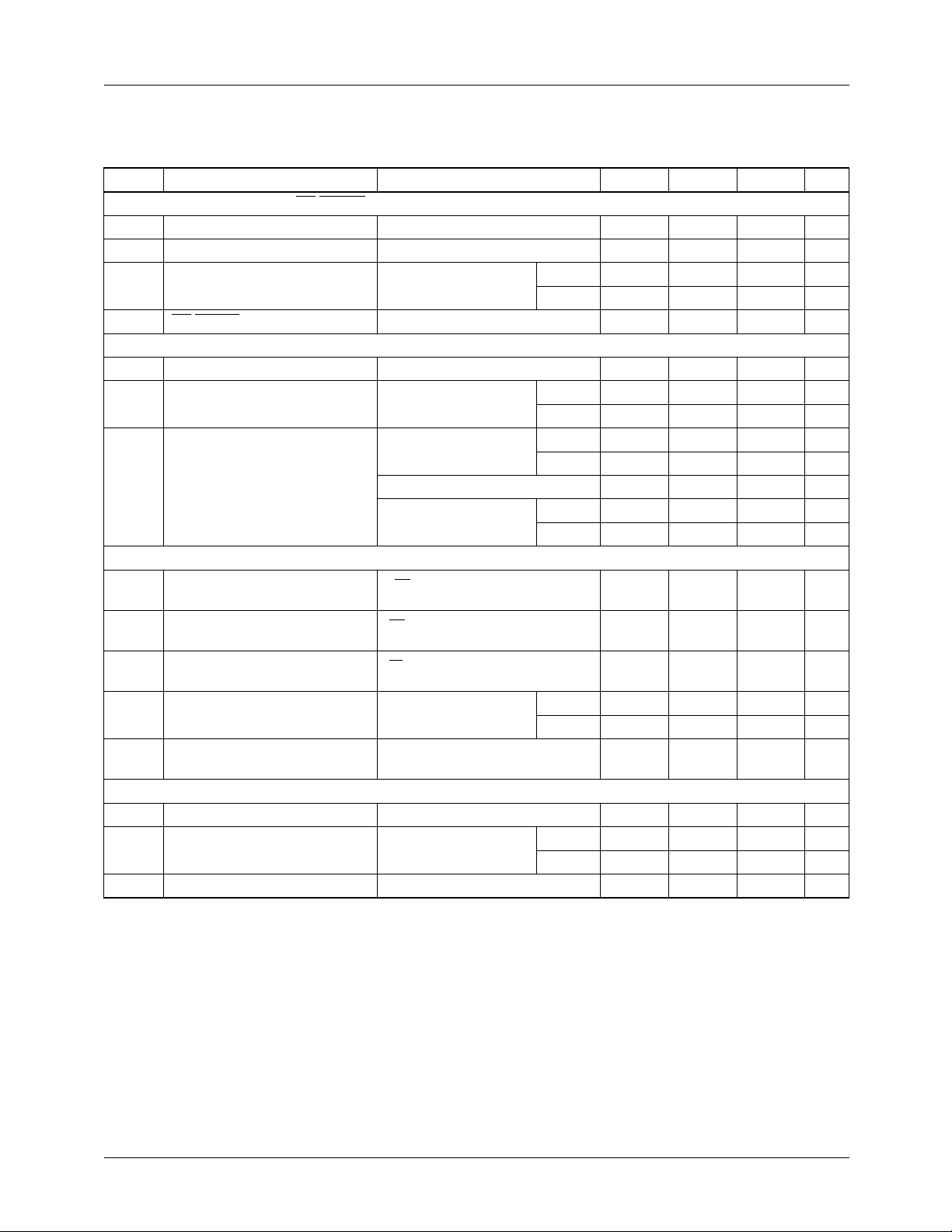
Parameter Min. Max. Units
V
DD
14 V
Logic Inputs (SPEED FB, BRAKE) GND – 0.3 7 V
All Other Inputs and Outputs GND – 0.3 V
Output Current (LA, LB, LC, HA
, HB, HC
+ 0.3 V
DD
±50 mA
Junction Temperature 150 °C
Storage Temperature Range -65 150 °C
Lead Temperature (Soldering 10 sec.) 260 °C
Thermal Resistance ( θ
28-Pin Narrow PDIP
28-Pin SOIC
JA
)
48
75
°C/W
°C/W
Operating Conditions
Parameter Min. Max. Units
Temperature Range
ML4425CX
ML4425IX
V
DD
0
–40
70
85
°C
°C
10.8 13.2 V
REV. 1.0.2 7/2/01
3
Page 4
) ≤
ML4425 PRODUCT SPECIFICATION
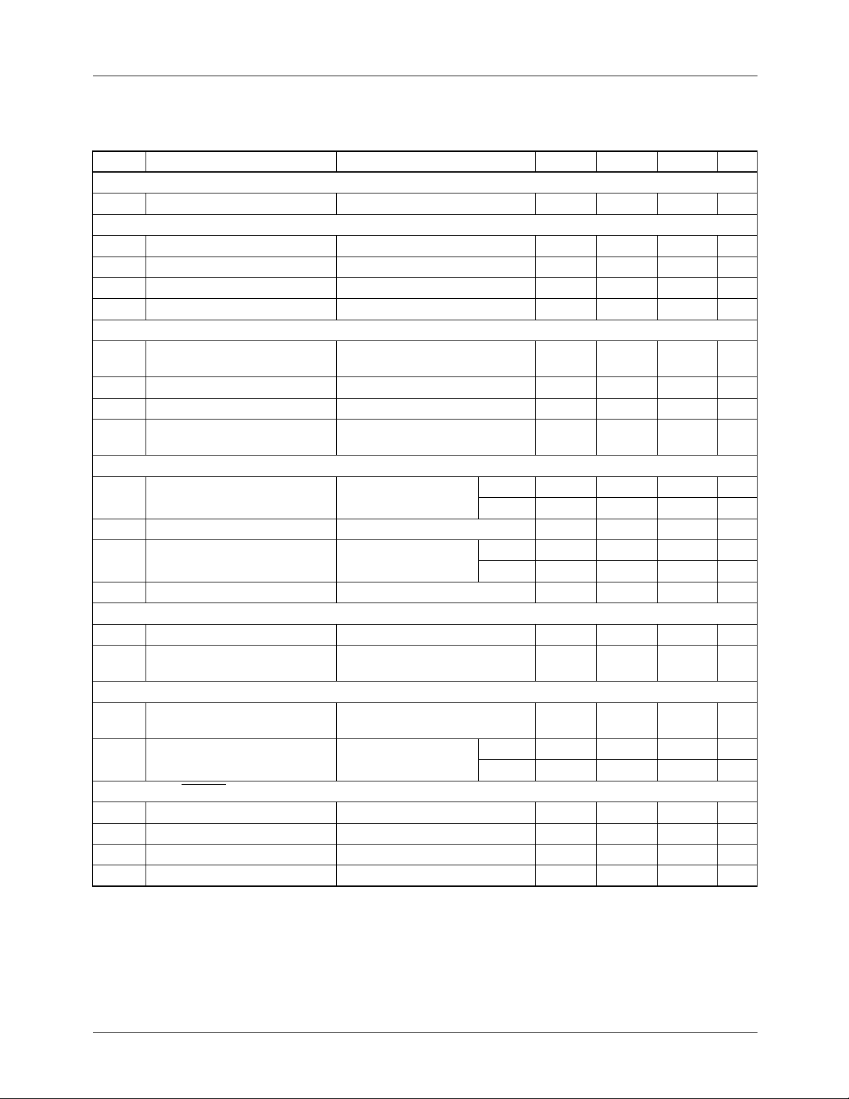
Electrical Characteristics
Unless otherwise specified, V
T
= Operating Temperature Range (Notes 1, 2) .
A
Symbol Parameter Conditions Min. Typ. Max. Units
Reference
V
Total Variation Line, Temp 6.5 6.9 7.5 V
REF
PWM Oscillator
Total Variation C
Ramp Peak 3.9 V
Ramp Valley 1.7 V
Ramp Charging Current µA
Speed Control Loop
SPEED SET Input Voltage
Range
SPEED FB Input Voltage Range 0 V
SPEED COMP Output Current ±5 ±20 µA
SPEED SET Error Amp
Transconductance
Start-up
C
Charging Current C Suffix 0.68 0.98 µA
AT
C
Threshold Voltage 1.4 1.7 V
AT
C
Charging Current C Suffix 0.68 0.98 µA
RT
C
Threshold Voltage 1.4 1.7 V
RT
Voltage Controlled Oscillator
Frequency Range R
Frequency vs. SPEED FB R
Current Limit
I
Gain V(I
SENSE
= 12V ± 10%, R
DD
= 1 Ω , C
SENSE
= 1nF 28 kHz
T
V
SPEED SET
V
SPEED FB
= xV,
= yV
VCO
= 10nF, C
= 100pF, R
IOS
= 137k Ω ,
REF
0V
REF
REF
144 µ
I Suffix 0.5 1.1 µA
I Suffix 0.5 1.1 µA
= 5V, SPEED FB = 6V 1.5 1.85 2.2 kHz
VCO
= 5V, 0.5V ≤ SPEED FB ≤
VCO
300 Hz/V
7V
2.5V 4.5 5.0 5.5 V/V
LIMIT
V
V
Ω
One Shot OFF-Time C
Logic Inputs (BRAKE) (Note 3)
V
V
Input High Voltage 2 V
IH
Input Low Voltage 0.8 V
IL
Input High Current V
I
IH
I
Input Low Current V
IL
4
= 100pF C Suffix 9 18 µs
IOS
I Suffix 9 20 µs
= 2.4V 2.4 mA
IH
= 0.4V 2.9 mA
IL
REV. 1.0.2 7/2/01
Page 5
PRODUCT SPECIFICATION ML4425
Electrical Characteristics (continued)
Unless otherwise specified, V
TA = Operating Temperature Range (Notes 1, 2).
Symbol Parameter Conditions Min. Typ. Max. Units
Logic Outputs (VCO/TACH, UV FAULT) (Note 3)
VCO/TACH Output High Voltage I
VCO/TACH Output Low Voltage I
UV FAULT Output High Voltage I
UV
FAULT Output Low Voltage I
Back-EMF Sampler
SPEED FB Align Mode Voltage 125 250 mV
SPEED FB Ramp Mode Current C Suffix 500 720 nA
SPEED FB Run Mode Current State A, C
Output Drivers
High Side Driver Output Low
Current
High Side Driver Output High
Voltage
Low Side Driver Output Low
Voltage
Low Side Driver Output High
Voltage
Phase C Cross-conduction
Lockout Threshold
Supply
I
DD
VDD Current 32 50 mA
UVLO Threshold C Suffix 8.8 9.5 10.2 V
UVLO Hysteresis 150 mV
Notes:
1. Limits are guaranteed by 100% testing, sampling, or correlation with worst case test conditions.
2. For explanation of states, see Figure 4 and Table 1.
3. The BRAKE and UV FAULT pins each have an internal 4k Ω resistor to the internal reference.
= 12V ± 10%, R
DD
= 1Ω, C
SENSE
= –100µA 2.2 V
OUT
= 400µA 0.6 V
OUT
= –10µA C Suffix 3.4 4.5 5.4 V
OUT
VCO
= 10nF, C
= 100pF, R
IOS
= 137kΩ,
REF
I Suffix 3.2 5.6 V
= 400µA 0.6 V
OUT
I Suffix 500 750 nA
= 5V,
V
PHB
State A, C
State A, C
V
PHB
V
HX
I
HX
I
LX
V(I
RT
= V
/3
DD
= 5V, V
RT
= 5V,
RT
= 2 ↔ V
DD
/3
= 2 V 0.5 1.2 mA
= –10µ AV
= 1mA 0.2 0.7 V
) = 0V C Suffix VDD – 2.2 V
SENSE
C Suffix 30 90 µA
I Suffix 27 90 µA
= V
PHB
/2 –15 15 µA
DD
C Suffix –90 –30 µA
I Suffix –90 –27 µA
– 1.3 V
CC
I Suffix V
– 2.9 V
DD
V
– 3.0 V
DD
I Suffix 8.6 10.3 V
REV. 1.0.2 7/2/01
5
Page 6

ML4425 PRODUCT SPECIFICATION
Functional Description
General
The ML4425 provides all the circuitry for sensorless speed
control of 3-phase Brushless DC (BLDC) motors. Controller
functions include start-up circuitry, back-EMF commutation
control, Pulse Width Modulation (PWM) speed control,
fixed OFF-time current limiting, braking, and undervoltage
protection.
The start-up circuitry aligns the motor to a known position,
then ramps up the motor speed to generate a back-EMF
signal. A back-EMF sampling circuit controls commutation
timing by forming a Phase Locked Loop (PLL). The commutation control circuitry also outputs a speed feedback
(SPEED FB) signal used in the speed control loop. The
speed control loop consists of an error amplifier and PWM
comparator that produce a PWM duty cycle for speed regulation. Motor current is limited by a fixed OFF-time PWM
shutdown comparator that is controlled by an external sense
resistor. Commutation control, PWM speed control, and
current limiting are combined to produce the output driver
signals. Six output drivers are used to provide gating signals
to an external 3 phase bridge power stage sized for the
BLDC motor voltage and current requirements. Additional
functions include a braking function and undervoltage
protection circuit to shut down the output drivers in the event
of a low voltage condition on V
of the ML4425.
DD
If one or more of the above values is not known, it is still
possible to pick components for the ML4425, but some
experimentation may be necessary to determine the optimal
values. All quantities are in SI units unless otherwise specified. The following formulas should be considered as a starting point for optimization. All calculations for capacitors and
resistors should be used as the first approximation for selecting the closest standard value.
Power Supply and Reference
The supply voltage (VDD) is nominally 12V ±10%. A 100nF
bypass capacitor to ground should be placed as close as possible to V
. A 6.9V voltage reference output (V
DD
REF
) is pro-
vided to set the speed command and current limit of the
ML4425. A 137kΩ from R
to GND is required to set up a
REF
reference current for internal functions.
Output Drivers
The output drivers LA, LB, LC, HA, HB, and HC provide
totem pole output drive signals for a 3 phase bridge power
stage. All control functions in the ML4425 translate to outputs at these pins. LA, LB, and LC provide the low-side
drive signals for phases A, B, and C of the 3 phase power
stage and are 12V active high signals. HA, HB, and HC
provide the high-side signals and are 12V active low signals.
V
MOTOR
12V
Component Selection
Selecting external components for the ML4425 requires
calculations based on the motor’s electrical and mechanical
parameters. The following is a list of the motor parameters
needed for these calculations :
• DC motor supply voltage – V
• Maximum operating current – I
• Number of magnetic poles – N
• Back EMF constant – Ke (V-s/Rad)
• Motor torque constant – Kt (Nm/A) (Kt = Ke in SI units)
• Maximum speed of operation RPM
• Moment of inertia of the motor and load – J (Kg-m2)
• Viscous damping factor of the motor and load – ζ
MOTOR
MAX
(V)
(A)
MAX
(RPM)
DC SUPPLY
CAPACITOR
HA
LA
Figure 1. Using R
HB
MOTOR
PHASE A
LB
R
SENSE
in a 3-Phase 12V Power Stage
SENSE
HC
MOTOR
PHASE B
LC
MOTOR
PHASE C
6 REV. 1.0.2 7/2/01
Page 7

PRODUCT SPECIFICATION ML4425
Current Limiting in the Power Stage
The current sense resistor (R
lates the maximum current in the power stage and the BLDC
motor. Current regulation is accomplished by shutting off the
output drivers LA, LB, and LC for a fixed amount of time if
the voltage across R
exceeds the current limit thresh-
SENSE
old.
I
LIMIT
The voltage on the I
pin sets the current limit threshold.
LIMIT
The ML4425 has an internal voltage divider from V
sets a default current limit threshold of 2.3V (see Figure 2).
An external voltage divider referenced to V
to override the default I
LIMIT
should have at least 10 times the current flow of the internal
divider.
R
SENSE
The function of R
is to provide a voltage proportional
SENSE
to the motor current to set the current limit trip point. The
default trip voltage across R
internal I
divider ratio. The current sense resistor
LIMIT
should be a low inductance resistor such as a carbon composition. For resistors in the milliohms range, wire-wound
resistors tend to have low values of inductance. R
should be sized to handle the power dissipation (I
R
).
SENSE
I
The I
SENSE
SENSE
Filter
RC lowpass filter is placed in series with the current sense signal as shown in Figure 2. The purpose of this
filter is to remove the diode reverse recovery shootthrough
current. This current causes a voltage spike on the leading
edge of the current sense signal which may falsely trigger the
current limit. The current sense voltage waveform is shown
before and after filtering in Figure 3. The recommended
) shown in Figure 1 regu-
SENSE
REF
can be used
REF
setting. The external divider
is 460mV, set by the
SENSE
SENSE
2
MAX
that
↔
starting values for this circuit are R = 1kΩ and C = 330pF.
This gives a time constant of 330ns, and will filter out spikes
of shorter duration. C can be increased to as much as 2.2nF,
but should not exceed a time constant of more than a few
microseconds.
C
IOS
When I
exceeds 0.2 ↔ I
SENSE
, the current limit one-
LIMIT
shot is activated, turning off LA, LB, and LC for a fixed
amount of time (t
tance connected to C
OFF
). t
is set by the amount of capaci-
OFF
. C
IOS
is usually set for a fixed off
IOS
time equal to or less than the PWM period. For a 25kHz
PWM frequency, the PWM period is 40µs; t
between 20µs and 40µs. The lower limit of t
should be
OFF
is dictated
OFF
by the minimum on time of the power stage; a safe approximation is 5µs or less. The equation for finding the C
IOS
capacitance value is as follows:
t
50µA×
OFF
---------------------------------=
C
OS
2.4V
(1)
Commutation Control
A 3-phase BLDC motor requires electronic commutation to
achieve rotational motion. Electronic commutation requires
the switching on and off of the power switches of a 3-phase
half bridge. For torque production to be achieved in one
direction, the commutation is dictated by the rotor position.
Electronic commutation in the ML4425 is achieved by turning on and off, in the proper sequence, one N output from
one phase and one P output from another phase. There are
six combinations of N and P outputs (six switching states)
that constitute a full commutation cycle. These combinations
are illustrated in Table 1 and Figure 4, and are labeled states
A through F. This sequence is programmed into the commutation state machine. Clocking of the commutation state
machine is provided by a voltage controlled oscillator
(VCO).
FROM
R
SENSE
I
V
REF
SENSE
I
LIMIT
16kΩ
V
× 5
REF
8kΩ
–
+
2.9V
0V
Figure 2. Current Sense Circuitry
C
STOP
START
IOS
SRQ
PWM
ON/OFF
Q
30µA
460mV
0V
(a)
Figure 3. Current Sense Resistor Waveforms
(a) Without Filtering, and (b) With Filtering
(b)
REV. 1.0.2 7/2/01 7
Page 8

ML4425 PRODUCT SPECIFICATION
State
LA LB LC HA HB HC
Outputs Input
Sampling
R OFF ON OFF ON OFF ON N/A
A OFF OFF ON ON OFF OFF FB B
B OFF OFF ON OFF ON OFF FB A
C ON OFF OFF OFF ON OFF FB C
D ON OFF OFF OFF OFF ON FB B
E OFF ON OFF OFF OFF ON FB A
F OFF ON OFF ON OFF OFF FB C
Table 1. Commutation State Functions
ABCDEFABCDEF
HA
HIGH
SIDE
DRIVE
OUTPUTS
HB
HC
LA
LOW
SIDE
DRIVE
OUTPUTS
LB
LC
Cycle 1 – Full Commutation, Cycle 2 – Commutation with 50% PWM Duty Cycle
Figure 4. Output Commutation Sequence Timing Diagram
Voltage Controlled Oscillator (VCO)
The VCO provides a TTL compatible clock output on the
VCO/TACH pin proportional to the VCO input voltage at the
SPEED FB pin. The proportion of frequency to voltage
(VCO constant, Kv) is set by an 80.6kΩ resistor on R
and a capacitor on C
as shown in Figure 5. R
VCO
VCO
a current proportional the VCO input voltage at SPEED FB.
This current is used to charge and discharge C
VCO
the threshold voltages of 2.3V and 4.3V. The resulting triangle wave on C
corresponds to the clock on VCO. Kv
VCO
should be set so that the VCO output frequency corresponds
VCO
sets up
between
to the maximum commutation frequency or maximum motor
speed when the VCO input is equal to or slightly less than
. C
V
REF
is calculated using the following equation:
VCO
Hz Farad•
6–
------------------------------
C
6.5V 3.101× 10
-----------------------------------------------------------------------------------=
VCO
0.05
Hz
--------------
RPM
×
×
N× SPEED
V
MAX
(2)
The closest standard value that is equal to or less than the
calculated C
should be used.
VCO
8 REV. 1.0.2 7/2/01
Page 9

PRODUCT SPECIFICATION ML4425
The maximum frequency on the VCO pin is found by:
f
MAX
0.05 N× RPM
×=
MAX
(3)
The voltage at the VCO/TACH pin is equal to the rotor
speed. The voltage at SPEED FB is controlled by the back
EMF sampler.
Back EMF Sampler
The input to the voltage controlled oscillator is the back
EMF sampler. The back EMF sense pins FB A, FB B, and
FB C inputs to the back EMF sampler require a signal from
the motor phase leads that is below the V
The phase sense input impedance is 8kΩ. This requires a
series resistor RES1 from the motor phase lead as shown in
Figure 6 based on the following equation:
RES1 670Ω V⁄ V
MOTOR
The back EMF sampler takes the motor phase voltages
divided down to signals that are less than V
nal) and calculates the neutral point of the motor by the following equation:
Neutral
PH1 PH2 PH3++
-------------------------------------------------=
3
This allows the ML4425 to compare the back EMF signal to
the motor’s neutral point without the need for bringing out an
extra wire on a WYE wound motor. For DELTA wound
motors there is no physical neutral to bring out, so this reference point must be calculated in any case.
of the ML4425.
DD
10V–()×=
(12V nomi-
DD
(4)
(5)
FROM
BACK EMF
SAMPLER
& RAMP
GENERATOR
C
VCO
VCO/TACH
RESET
(FROM CAT)
4.3V
2.3V
5V
0V
C
VCO
SPEEDFBC
VCO
VOLTAGE
CONTROLLED
OSCILLATOR
R
VCO
R
VCO
VCO/TACH
Figure 5. External VCO Component Connections
The back EMF sampler measures the motor phase that is not
driven (i.e. if LA and HB are on, then phase A is driven low,
phase B is driven high, and phase C is sampled). The sampled phase provides a back EMF signal that is compared
against the neutral of the motor. The sampler is controlled by
the commutation state machine. The sampled back EMF is
compared to the neutral through an error amplifier. The output of the error amplifier outputs a charging or discharging
current to SPEED FB, which provides the control voltage to
the VCO.
MOTOR ΦA
MOTOR ΦB
MOTOR ΦC
F/R
RES1
RES2
RES3
FB A
FB B
FB C
F/R
4kΩ
4kΩ
4kΩ
4kΩ
4kΩ
4kΩ
NEUTRAL
SIMULATOR
ΦA + ΦB + ΦC
6
MULTIPLEXER
SIGN
CHANGER
COMMUTATION
STATE MACHINE
gm =
+
–
8kΩ
1
TO
SPEED FB
Figure 6. Back EMF Sampler Detailed Block Diagram
REV. 1.0.2 7/2/01 9
Page 10

ML4425 PRODUCT SPECIFICATION
Back EMF Sensing PLL Commutation Control
Three blocks form a phase locked loop that locks the commutation clock onto the back EMF signal: the commutation
state machine, the voltage controlled oscillator, and the back
EMF sampler. The complete phase locked loop is illustrated
in Figure 7. The phased locked loop requires a lead lag filter
that is set by external components on SPEED FB. The components are selected as follows:
C
SPEEDFB1
0.25
K
O1
-------------------------------------------------
----------
××=
M
In
N
S
2
d
----------
100
2
(6a)
2
f
×
VCO
FB A
22
FB B
23
FB C
24
SAMPLER
BACK
EMF
500nA
SPEED
FB
V
DD
C
SPEEDFB1
20
VOLTAGE
CONTROLLED
OSCILLATOR
R
SPEEDFB
C
SPEEDFB2
VCO/TACH
13
R
SPEEDFB
C
SPEEDFB2CSPEEDFB1
2= MIn
××
= M1–()×
d
----------
×
100
f
VCO
-------------------------------------------------NSKO1× 1M–()×
(6b
(6c)
Start-Up Sequence
When power is first applied to the ML4425 and the motor is
at rest, the back EMF is equal to zero. The motor needs to be
rotating for the back EMF sampler to lock onto the rotor
position and commutate the motor. The ML4425 uses an
open loop start-up technique to bring the rotor from rest up
to a speed fast enough to allow back EMF sensing. Start-up
is comprised of three modes: align mode, ramp mode, and
run mode.
Align Mode (RESET)
Before the motor can be started, the rotor must be in a known
position. When power is first applied to the ML4425, the
controller is reset into the align mode. Align mode turns on
the output drivers LB, HA, and HC which aligns the motor
into a position 30 electrical degrees before the center of the
first commutation state. This is shown as state R in the commutation states of Table 1. Align mode must last long enough
to allow the motor and its load to settle into this position. The
align mode time is set by a capacitor connected to the CAT
pin as shown in Figure 8. CAT is charged by a constant
750µA current from GND to 1.5 V until the align comparator
trips to end the align mode. A starting point for CAT is calculated as follows:
tS7.5× 107–amp××
--------------------------------------------------------=
C
AT
1.5V
If the align time is not long enough to allow the rotor to settle
for reliable starting, then increase C
until the desired per-
AT
formance is achieved.
(7)
R
A
F
E
COMMUTATION
STATE MACHINE
B
C
D
PHASE
LOCKED
LOOP
Figure 7. Back EMF Commutation Phase Locked Loop
Ramp Mode
At the end of align mode the controller goes into ramp mode.
Ramp mode starts commutating through the states A through
F as shown in Table 1. This ramps up the commutation frequency, and therefore the motor speed, for a fixed length of
time. This allows the motor to reach a sufficient speed for the
back EMF sampler to lock commutation onto the motor’s
back EMF. The amount of time the ML4425 stays in ramp
mode is determined by a capacitor connected to the CRT pin
as shown in Figure 8. C
current from GND to 1.5 V until the ramp comparator trips
to end the ramp mode. This gives a fixed ramp time. CRT is
calculated as follows:
C
RT
The rate at which the ML4425 ramps up the motor speed is
determined by a fixed 500µA current source on the SPEED
FB pin. The current sources charges up the PLL filter components causing the VCO frequency to ramp up. During
ramp mode, the back EMF sampler is disabled to allow control of the ramping to be set only by the 500µA current
source. The ramp based on the SPEED FB filter is generally
too fast for the motor to keep up, so a capacitor from CRR to
SPEED FB can be added to slow down the ramping rate. The
optimal ramp rate is based on the motor and load parameters
and is can be adjusted by varying the value of CRR.
is charged by a constant 750µA
RT
2π J× 5× 10⁷–× amp× KV×
----------------------------------------------------------------------------=
I
× 3× N×
MAXKt
(8)
10 REV. 1.0.2 7/2/01
Page 11

PRODUCT SPECIFICATION ML4425
C
FB A
FB B
FB C
750nA
BACK
EMF
SAMPLER
RR
C
AT
V
750nA
DD
1.5V
C
RT
C
DD
1.5V
AT
–
+
TO RESET INPUT
OF COMMUTATION
STATE MACHINE
V
C
RT
C
RR
–
+
500nA
V
DD
SPEED FB
SPEED
FB
TO
FILTER
C
VCO
VOLTAGE
CONTROLLED
OSCILLATOR
R
VCO
VCO/TACH
Figure 8. ML4425 Start-up Circuitry for Controlling the Align and Ramp Times
Run Mode (Back EMF Sensing)
At the end of ramp mode the controller goes into run mode.
In run mode, the back EMF sensing is enabled and commutation is now under the control of the phase locked loop. Motor
speed is now regulated by the speed control loop.
PWM Speed Control
Speed control is accomplished by setting a speed command
at SPEED SET with an input voltage from 0 to 6.9V (V
The accuracy of the speed command is determined by the
external components R
VCO
and C
. There are a number of
VCO
methods that can be used to control the speed command of
the ML4425. One is to use a 10kΩ potentiometer from V
to ground with the wiper connected to SPEED SET. If
SPEED SET is controlled from a microcontroller, one of its
DACs can be used with V
as its input reference.
REF
The speed command is compared with the sensed speed from
SPEED FB through a transconductance error amplifier. The
output of the speed error amplifier is SPEED COMP. SPEED
COMP is clamped between one diode drop above 3.9V
(approximately 4.6V) and one diode drop below 1.7V
(approximately 1V) to prevent speed loop “wind-up”. Speed
loop compensation components are connected to this pin as
shown in Figure 9. The speed loop compensation components are calculated as follows:
26.9 N V
-------------------------------------------------------------------------------------------=
C
SC
f
× 2.5 98.696 τm2f
SBKe
10
SC
---------------------------------------=
2π f
××
SBCSC
R
×××
MOTORCVCO
2
××+
SB
REF
REF
(9a)
(9b)
).
FROM
SPEED FB
V
REF
10kΩ
R
SC
C
SC
C
T
SPEED SET
SPEED COMP
C
+
–
3.9V
–
+
1.7V
T
1.7V
20kHz
PWM ON/OFF
FROM I
ONE-SHOT
Figure 9. Speed Control Loop Component Connections
The voltage on SPEED COMP is compared with a ramp
oscillator to create a PWM duty cycle. The PWM ramp oscillator creates a sawtooth function from 1.7V to 3.9V as shown
in Figure 9. A negative clamp at one diode drop below 1.7V
(approximately 1V) starts the oscillator on power up. The
frequency of the ramp oscillator is set by a capacitor to
ground C
Where f
and is selected using the following equation:
IOS
I
--------------
50µA×
f
PWM
-----------------------------------=
C
T
is the PWM frequency in Hz. The PWM duty
PWM
2.4V
cycle from the speed control loop is gated the current limit
one shot that controls the LA, LB, and LC output drivers.
DRIVERS
LIMIT
TO
GATING
LOGIC &
OUTPUT
(10)
Where fSB is the speed loop bandwidth in Hz.
REV. 1.0.2 7/2/01 11
Page 12

ML4425 PRODUCT SPECIFICATION
Cross Conduction Comparator
When the ML4425 goes from align mode into ramp mode,
there is a possibility of cross conduction in phase 3 of the
bridge power stage. This cross conduction can happen when
HC
is on in the align mode shown as state R in Table 1, and
the controller transitions to state A in ramp mode where HC
is turned off and LC is turned on. Cross conduction can
appear due to the differences in turn on and turn off times of
the power devices. To solve this problem, the LC output
driver is gated off until the HC is equal to V
DD
– 3V as
shown in Figure 10.
Braking
When the BRAKE pin is pulled below 1.4V, the low side
output drivers LA, LB, and LC are turned on and the high
side output drivers HA, HB, HC are turned off. Braking
causes rapid deceleration of the motor and current limiting is
de-activated, and care should be taken when using the
BRAKE pin. BRAKE is has an internal 4kΩ pull-up as
shown in Figure 10, and can be driven by a switch to ground,
an open collector or drain logic signal, or a TTL logic signal.
Undervoltage Lockout
Undervoltage lockout is used to protect the 3-phase bridge
power stage from a low VDD condition. Undervoltage is triggered at VDD of 9.5V or less and is indicated by a TTL low
output on the UV FAULT pin. Undervoltage lockout also
turns off all output drivers (LA, LB, LC, HA, HB, and HC).
The comparator that triggers undervoltage lockout has
150mV of hystresis.
The most flexible configuration is to use high side drivers to
control N-Channel MOSFETs (or IGBTs) which allows
applications from less than 12V up to 600V. Figure 12 shows
the interface between the ML4425 and IR2118 high side
drivers from International Rectifier. This configuration is
capable of driving motors from busses of up to 320V. The
BRAKE
pin can be pulsed prior to startup with an RC
circuit. This charges the bootstrap capacitors (C19, C20, and
C21) for the three high side drivers, allowing the reset phase
to operate normally. These capacitors must be sized so that
they stay sufficiently charged during the align mode. Refer to
AN-43 for additional applications information on the
ML4425.
FROM
COMMUTATION
STATE MACHINE
FROM
SPEED CONTROL LOOP
& CURRENT LIMIT
–
1.4V
BRAKE
25
+
V
DD
4kΩ
9.5V
+
–
REFERENCE
V
DD
14
28
GATING
LOGIC
OUTPUT
DRIVERS
GND27R
&
REF
V
REF
7
HA
HB
HC
LA
LB
LC
UV FAULT
2
3
4
9
10
11
18
Design Considerations
Interfacing to a 3-Phase Bridge Power Stage
The ML4425 output drivers are configured to drive a 3 phase
bridge power stage. For applications with buss voltages from
12V up to 80V, level shifting circuitry can be used to drive
higher voltage P-channel MOSFETS for the high side
switches as shown in Figure 11.
Figure 10. Cross Conduction, Brake, and UVLO Circuits
12 REV. 1.0.2 7/2/01
Page 13

PRODUCT SPECIFICATION ML4425
V
BUSS
24V–80V
12V
C2
330µF
100V
100nF
100V
Q1
TN6718A
C3
1µF
C1
R2
10kΩ
Q4
FQD8P10
Q2
TN6718A
R3
10kΩ
Q5
FQD8P10
Q3
TN6718A
R4
10kΩ
Q6
FQD8P10
R12
2kΩ
R16
10kΩ
C9
100nF
100Ω
Q7
IRFR120
R1
470mΩ
2W
R13
2kΩ
Q8
IRFR120
R14
2kΩ
R15
1kΩ
Q9
IRFR120
C5
2.2nF
MOTOR
ML4425
I
SENSE
HA
HB
HC
SPEED COMP
C
C17
1nF
C12
R7
R5
100Ω
R6
100Ω
12V
R18
10kΩ
R21
787Ω
C14
1µF
V
SPEED SET
LA
LB
LC
I
VCO/TACH
V
C13
100nF
T
REF
LIMIT
DD
GND
R
REF
C
IOS
BRAKE
FB C
FB B
FB A
C
RR
SPEED FB
C
RT
UV FAULT
C
AT
R
VCO
C
VCO
R20
137kΩ
C16
330pF
R8 (RES1)
R9 (RES1)
R10 (RES1)
C14
R17
10kΩ
C8
C6
1µF
1µF
R19
C4
80.5kΩ
100nF
470nF
RUN
S1
BRAKE
C7
C15
Figure 11. Driving Lower Voltage Motors (12 to 80V)
REV. 1.0.2 7/2/01 13
Page 14

ML4425 PRODUCT SPECIFICATION
12V
V
BUSS
24V–80V
C5
330µF
400V
C16
100nF
25V
R6
100Ω
Q1
FQP4P40
IR2118
V
CC
IN
HO
COM
NC
NC
Q2
FQP5N40
R12
470mΩ
2W
VB
VS
D1
MUR150
C19
2.2µF
25V
R7
100Ω
Q3
FQP4P40
C17
100nF
25V
Q4
FQP5N40
IR2118
V
CC
IN
COM
NC
R8
100Ω
Q5
FQP4P40
VB
HO
VS
NC
Q6
FQP5N40
D2
MUR150
C20
2.2µF
25V
100nF
MOTOR
C18
25V
IR2118
V
CC
IN
HO
COM
NC
NC
VB
VS
D3
MUR150
C21
2.2µF
25V
D4 D5 D6
R5
10kΩ
C3
100nF
100Ω
(3×1N5819)
R9
R10
100Ω
100nF
R11
100Ω
C4
1nF
C15
12V
R20
10kΩ
R19
787Ω
C6
1µF
R1
1kΩ
I
SENSE
HA
HB
HC
SPEED COMP
C
T
V
REF
SPEED SET
LA
LB
LC
I
LIMIT
VCO/TACH
V
DD
C7
100nF
C1
2.2nF
ML4425
RAMP COMP
SPEED FB
UV FAULT
GND
R
REF
C
IOS
BRAKE
FB C
FB B
FB A
C
RT
C
AT
R
VCO
C
VCO
C8
10nF
R18
137kΩ
R15 (RES1)
R14 (RES1)
C13*
C10
1µF
80.6kΩ
C14
330pF
R13 (RES1)
R17
10kΩ
C12
1µF
R16
PRE-CHARGE
C11
100nF
C9
470nF
BOOTSTRAP
CAPACITOR
RUN
S1
BRAKE
Figure 12. ML4425 High Voltage Motor Drive Application Circuit
14 REV. 1.0.2 7/2/01
Page 15

PRODUCT SPECIFICATION ML4425
3
Mechanical Dimensions inches (millimeters)
Package: P28N
28-Pin Narrow PDIP
1.355 - 1.365
(34.42 - 34.67)
28
0.180 MAX
(4.57 MAX)
0.125 - 0.135
(3.18 - 3.43)
28
PIN 1 ID
1
0.699 - 0.713
(17.75 - 18.11)
0.045 - 0.055
(1.14 - 1.40)
0.015 - 0.021
(0.38 - 0.53)
Package: S28
28-Pin SOIC
0.100 BSC
(2.54 BSC)
SEATING PLANE
0.280 - 0.296
(7.11 - 7.52)
0.020 MIN
(0.51 MIN)
0.299 - 0.325
(7.60 - 8.26)
0º - 15º
0.008 - 0.012
(0.20 - 0.31)
0.024 - 0.034
(0.61 - 0.86)
(4 PLACES)
0.090 - 0.094
(2.28 - 2.39)
0.291 - 0.301
(7.39 - 7.65)
PIN 1 ID
1
0.050 BSC
(1.27 BSC)
0.012 - 0.020
(0.30 - 0.51)
0.095 - 0.107
(2.41 - 2.72)
SEATING PLANE
0.398 - 0.412
(10.11 - 10.47)
0.005 - 0.013
(0.13 - 0.33)
0º - 8º
0.022 - 0.042
(0.56 - 1.07)
0.009 - 0.01
(0.22 - 0.33)
REV. 1.0.2 7/2/01 15
Page 16

ML4425 PRODUCT SPECIFICATION
Ordering Information
Part Number Temperature Range Package
ML4425CP 0°C to 70°C 28-Pin PDIP (P28N)
ML4425CS 0°C to 70°C 28-Pin SOIC (S28)
ML4425IP -40°C to 85°C 28-Pin PDIP (P28N)
ML4425IS -40°C to 85°C 28-Pin SOIC (S28)
DISCLAIMER
FAIRCHILD SEMICONDUCTOR RESERVES THE RIGHT TO MAKE CHANGES WITHOUT FURTHER NOTICE TO
ANY PRODUCTS HEREIN TO IMPROVE RELIABILITY, FUNCTION OR DESIGN. FAIRCHILD DOES NOT ASSUME
ANY LIABILITY ARISING OUT OF THE APPLICATION OR USE OF ANY PRODUCT OR CIRCUIT DESCRIBED HEREIN;
NEITHER DOES IT CONVEY ANY LICENSE UNDER ITS PATENT RIGHTS, NOR THE RIGHTS OF OTHERS.
LIFE SUPPORT POLICY
FAIRCHILD’S PRODUCTS ARE NOT AUTHORIZED FOR USE AS CRITICAL COMPONENTS IN LIFE SUPPORT DEVICES
OR SYSTEMS WITHOUT THE EXPRESS WRITTEN APPROVAL OF THE PRESIDENT OF FAIRCHILD SEMICONDUCTOR
CORPORATION. As used herein:
1. Life support devices or systems are devices or systems
which, (a) are intended for surgical implant into the body,
or (b) support or sustain life, and (c) whose failure to
perform when properly used in accordance with
instructions for use provided in the labeling, can be
reasonably expected to result in a significant injury of the
user.
www.fairchildsemi.com
2. A critical component in any component of a life support
device or system whose failure to perform can be
reasonably expected to cause the failure of the life support
device or system, or to affect its safety or effectiveness.
7/2/01 0.0m 003
2001 Fairchild Semiconductor Corporation
Stock#DS300042003
 Loading...