

Page 1

July 2000
ML4423*
1, 2, or 3-Phase Variable Speed AC Motor Controller
GENERAL DESCRIPTION
The ML4423 provides the PWM sinewave drive signals
necessary for controlling three phase AC induction motors as
well as single and two phase split capacitor AC induction
motors.
A constant voltage/frequency ratio can be maintained
over a frequency range of greater than 10:1, providing
15Hz to 150Hz control. The output variable frequency AC
voltages are sensed and fed back to the controller to track the
sinewave frequency and amplitude set at the speed control
input. Direction, on two and three phase motors, is controlled
by changing the relative phase difference between the motor
windings: 90× for two phase motors and 120× and 240× for three
phase motors.
To protect the motor, power devices, high voltage drivers
and control circuitry, the ML4423 includes fixed period,
pulse by pulse variable duty cycle current limit, deadtime
circuitry, and undervoltage lockout. The ML4423 has
selectable output voltage swing of 5V or 12V for
interfacing to different high side drivers and power devices.
FEATURES
■ Drives single, two, and three phase AC motors
■ Greater than 10:1 variable speed control range
■ Constant V/F ratio with programmable end points
■ Reverse capability for two and three phase motors
■ Low distortion PWM sinewave drive
■ Eliminates run capacitors in PSC motors
■ Coast function for quick power disable
■ Low cost interface for various gate drivers
■ PWM current limit, undervoltage lockout, and
programmable deadtime
■ 12V ±20% operation with onboard 8V reference
(* Indicates Part Is End Of Life As Of July 1, 2000)
BLOCK DIAGRAM
FB A
1
FB C
2
FB B
3
C
12
V
5
V
4
R
6
O
SPEED
MIN
SPEED
+
–
+
–
+
–
+
–
SPEED
CONTROL
SINE A-C
27
GENERATOR
GENERATOR
28
SINE A
SINE B
SINE B-C
GENERATOR
13
PWM
OSCILLATOR
SINE C
F/R
PWM
SINE
WAVE
CONTROL
18
3PH/2PH
UVLO
26
COAST
14
R
DT
9
5V/12 SELECT
GATING
LOGIC
&
OUTPUT
DRIVERS
+
COMP
–
REFERENCE
V
DD
GND R
17 8 7
REF
I
SENSE
0.5V
V
REF
HA
HB
HC
LA
LB
LC
25
24
22
23
21
19
20
16
C
T
15
1
Page 2
ML4423
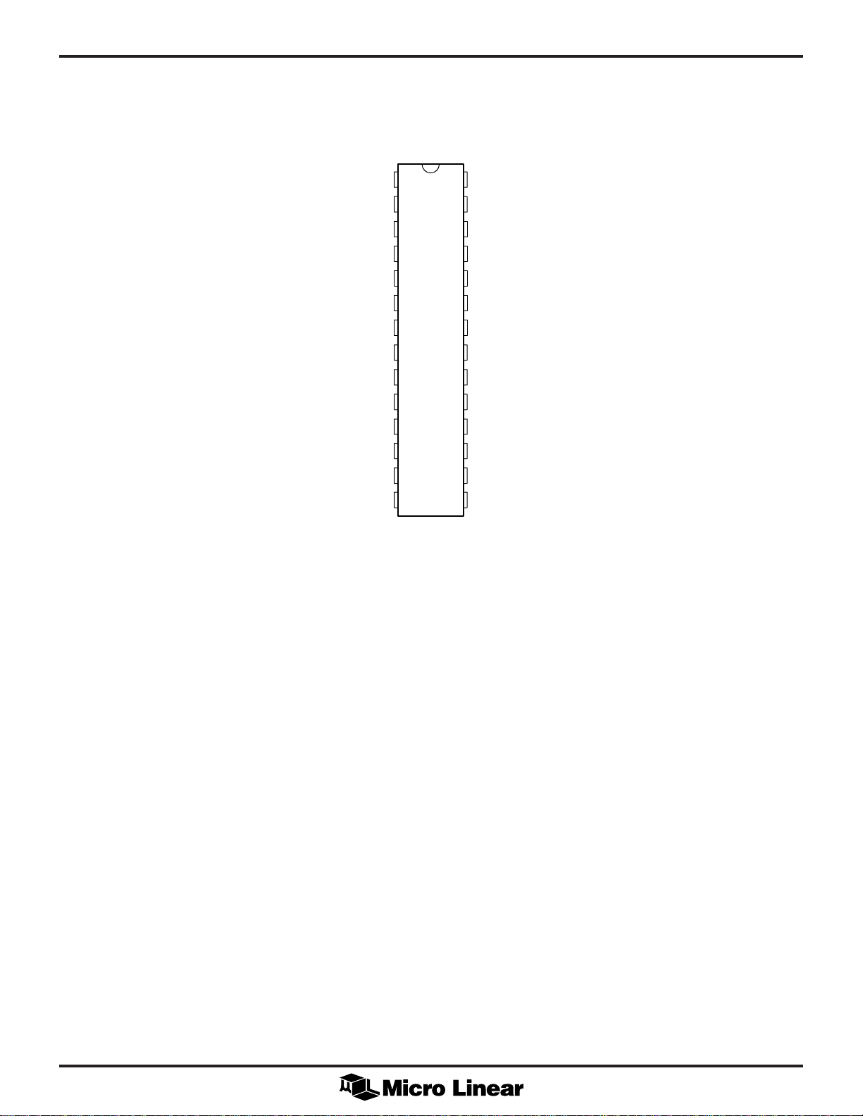
PIN CONFIGURATION
ML4423
28-Pin Narrow PDIP (P28N)
28-Pin SOIC (S28)
SENSE A
SENSE C
SENSE B
V
MIN
V
SPEED
R
SPEED
V
REF
R
REF
R
DT
SINE A-C
1
2
3
4
5
6
7
8
9
10
28
C
GM2
27
C
GM1
26
V
DD
25
5V/12V SELECT
24
HA
23
HC
22
HB
21
LA
20
LC
19
LB
SINE B-C
C
C
COAST
11
12
O
03
T
14
TOP VIEW
18
17
16
15
3PH/2PH
GND
I
SENSE
F/R
2
Page 3

PIN DESCRIPTION
ML4423
PIN NAME FUNCTION
1 FB A Differential input which, in
conjunction with FB C, feeds back the
voltage applied across motor winding
A-C.
2 FB C Input which feeds back the voltage
applied to motor winding C. Reference
voltage for windings A and B.
3 FB B Differential input which, in
conjunction with FB C, feeds back the
voltage applied across motor winding
B-C.
4V
MIN
The voltage on this pin sets the
minimum sinewave amplitude at low
speeds.
5V
SPEED
The voltage on this pin sets the
frequency and amplitude of the
sinewaves generated at SINEA and
SINEB.
6R
SPEED
An external resistor to ground provides
a variable current to the sinewave
generator. The current is proportional
to V
SPEED
.
PIN NAME FUNCTION
13 C
T
An external capacitor to ground sets
the PWM triangle frequency in
conjunction with the external resistor
R
.
REF
14 COAST A logic low input causes all output
drive transistors to turn OFF. An
internal pull-up drives COAST to V
if left unconnected.
15 F/R A logic high input causes phase A to
lead phase B, while a logic low input
causes phase A to lag phase B. An
internal pull-up drives F/R to VDD if
left unconnected.
16 I
SENSE
Motor current sense input.
17 GND Signal and power ground.
18 3PH/2PH Leaving this pin unconnected selects
3-phase drive. Connecting this pin to
VDD selects single/2-phase drive.
19 LB Low side drive output for phase B.
20 LC Low side drive output for phase C.
DD
7V
8R
REF
REF
8V reference output which can be
used for setting V
SPEED
and V
An external resistor to ground provides
a constant current used for setting the
PWM frequency in conjunction with
CT.
9R
DT
An external resistor to ground sets the
deadtime in the output stage to
prevent cross-conduction in the power
devices.
10 SINE A-C A test output for observing the
internally generated sinewave used for
motor winding A-C.
11 SINE B-C A test output for observing the
internally generated sinewave used for
motor winding B-C.
12 C
O
An external capacitor to ground sets
the sinewave frequency in conjunction
with V
SPEED
and R
SPEED
.
MIN
21 LA Low side drive output for phase A.
.
22 HB High side drive output for phase B.
23 HC High side drive output for phase C.
24 HA High side drive output for phase A.
25 5V/12V Input to select 5V or 12V output drive.
SELECT Leaving this pin unconnected selects
5V output drive levels at the driver
outputs. Connecting this pin to V
CC
selects 12V output drive levels at the
driver outputs.
26 V
27 C
DD
GM1
12V power supply input.
An external capacitor to ground sets a
pole in the feedback loop.
28 C
GM2
An external capacitor to ground sets a
pole in the feedback loop.
3
Page 4

ML4423
ABSOLUTE MAXIMUM RATINGS
Absolute maximum ratings are those values beyond which
the device could be permanently damaged. Absolute
maximum ratings are stress ratings only and functional
Thermal Resistance (qJA)
Plastic DIP ....................................................... 52ºC/W
Plastic SOIC .................................................... 75ºC/W
device operation is not implied.
V
.............................................................................................. 15V
DD
OPERATING CONDITIONS
Output Drive Current ........................................... ±50mA
Logic Inputs (F/R, COAST) .............................. –0.3 to 7V
Junction Temperature.............................................. 150ºC
Storage Temperature Range ...................... –65ºC to 150ºC
Lead Temperature (Soldering 10 sec) ...................... 260ºC
Temperature Range
C Suffix ...................................................... 0ºC to 70ºC
I Suffix ....................................................–40ºC to 85ºC
VDD...........................................................9.6V to 14.4V
ELECTRICAL CHARACTERISTICS
Unless otherwise specified, VDD = 12V ± 20%, R
C0 = 0.47mF, C
SYMBOL PARAMETER CONDITIONS MIN TYP MAX UNITS
REFERENCE
V
DIGITAL INPUTS
Output Voltage 7.6 7.8 8.2 V
REF
Line Regulation
Total Variation Line, Temperature
= 220pF, RDT = 166kW, TA = Operating Temperature Range (Note 1).
PWM
= 160kW, R
SPEED
= 250mW, R
SENSE
= 200kW,
REF
V
V
OUTPUT DRIVERS
V
V
SINE WAVE GENERATOR
V
PWM GENERATOR
CURRENT LIMIT
UNDERVOLTAGE LOCKOUT
Input Low Voltage 0.8 V
IL
Input High Voltage 2 V
IH
Output Low Voltage IOL = 20mA, 5V/12V SELECT = V
OL
Output High Voltage IOL = –20mA, 5V/12V SELECT = V
OH
Peak Voltage V
PP
Frequency V
Distortion 5%
Ramp Frequency 25 kHz
Threshold Voltage 0.4 0.5 0.6 V
Threshold Voltage 7.8 8.4 9.2 V
DD
I
= 2mA, 5V/12V SELECT = open 0.1 V
OL
DD
IOL = –2mA, 5V/12V SELECT = open 5 V
= 4.4V 3.4 V
SPEED
= 4.4V 60 Hz
SPEED
1V
V
– 1 V
DD
Hysteresis 0.5 V
SUPPLY
I
Note 1:
CC
VCC Operating Current 10 14 20 mA
Limits are guaranteed by 100% testing, sampling, or correlation with worst-case test conditions.
4
Page 5

FUNCTIONAL DESCRIPTION
ML4423
The ML4423 generates 2 reference sinewaves separated
by 90º or 60º in a closed loop feedback system. These
sinewaves can be varied in amplitude and frequency by
the speed input. Signals across the motor windings are fed
back and the ML4423 drives the external power output
stage with the PWM sinewave signal necessary to cause
the measured (feedback) output waveform to match the
internal reference sinewaves. The ML4423 provides fixed
period, variable duty cycle current limit protection, and
a programmable dead time circuit to prevent cross
conduction in the power output stage. An undervoltage
lockout circuit turns off the external power transistors if
VDD falls below 9V.
CIRCUIT BLOCKS AND COMPONENT SELECTION
R
REF
R
should be set to 200kW. This current along with
REF
C
set the PWM frequency.
PWM
Speed Control
The voltage on V
(pin 5) controls the sinewave
SPEED
frequency and amplitude. A 160kW resistor to ground on
R
(pin 6) converts the voltage on V
SPEED
to a current
SPEED
which is used to control the frequency of the output PWM
sinewaves. The amplitude of the sinewaves increases
linearly with V
until it reahces 4.4V. Above this
SPEED
voltage the amplitude remains constant and only the
frequency changes as shown in Figures 1 and 2.
SINEA and SINEB Generators
The capacitor to ground on C0 sets the frequency of the
sinewave according to the following relationship. C
0
should be a low temperature coefficient capacitor for
stable output frequency.
.
C
×108 800
0
= 58.7Hz and
SINE
(1)
(2)
For R
With V
V
f
SINE
= 160kW
SPEED
f
SINE
= 3V and C0 = 0.47mF, f
SPEED
R
=
4 0 170
CV
0
V
SPEED
=
,
SPEED
SPEED
×
can be observed at test points SINEA (pin 10) and SINE
(pin 11).
PWM Generator
A triangular PWM frequency will be generated on a
capacitor to ground on C
(pin 13). The frequency is
PWM
set by the following equation:
f
PWM
=
200 000,
1
C
×
PWM
(3)
B
150
120
90
60
FREQUENCY (Hz)
30
02468
V
Figure 1. Frequency vs V
SPEED
R
SPEED = 160
C0 = 0.47µF
(V)
SPEED
For C
= 220pF, f
PWM
1.25
1.00
0.75
0.50
NORMALIZED OUPTUT (V)
0.25
0
= 22.7kHz. It is recommended
PWM
4.4V
24
V
(V)
SPEED
Figure 2. Normalized Output Voltage vs V
68
SPEED
5
Page 6

ML4423
Current Limit
Motor current is sensed on I
SENSE
(pin 16). R
LIMIT
should
be selected so that
V
R
LIMIT
For a 2A current limit, R
05.
=
I
MAX
= 0.25W. The 1kW resistor
LIMIT
(4)
and 330pF capacitor filter (shown in figure 3) filter the
high frequency flyback pulses (due to the freewheeling
diode recovery currents) occurring at the output. When
I
is reached the output power will be turned off for
MAX
the remainder of the current PWM cycle, which is
asynchronous with the sinewave frequency. Thus current
limit is fixed-period with variable duty cycle.
PWM SINE Controller
This circuit block compares the sinewaves at SINEA and
SINEB to the sampled inputs SENSEA–SENSEC and
SENSEB–SENSEC, respectively. The PWM loop then
drives the outputs to force these “differential” waveforms
to equal the internal reference waveforms at SINEA and
SINEB. The differential signals SENSEA–SENSEC and
SENSEB–SENSEC will be approximately 1.7 volts zeropeak maximum. The signals at these pins should be
filtered to remove the PWM frequency. The high voltages
at the motor terminals are divided down to 1.7V to
provide voltage feedback to the controller. In figure 3,
the resistors to ground from SENSEA (pin 1) and SENSE
B
(pin 3) should be 1kW. SENSEC (pin 2) should have a
500W to ground because it has 1/2 the input impedance
of the other 2 inputs. The 0.15mF capacitors to ground on
SENSEA and SENSEB and the 0.3mF capacitor to ground
on SENSEC will create a 1kHz low pass filter at these
inputs. V
on the motor is set by the divider ratios.
PEAK
OUTPUT DRIVE
The 6 output drivers of the ML4423 drive the H and L
outputs from 0 to 12 volts (with pin 25 tied to VCC+(12V)).
The outputs will drive about 10mA and are designed to
drive output buffers and high side drivers requiring 12V
swings. The ML4423 provides lower current 0 to 5V drive
for high/low side drivers requiring 5V input signal swings
with pin 25 left unconnected.
PROGRAMMABLE DEADTIME
A dead time circuit is provided to prevent shoot through
currents in the power output stage. The dead time is
controlled by a resistor to ground on RDT (pin 9). The dead
time selected should be large enough to prevent cross
conduction between the upper and lower power devices
of each inverter phase leg.
−
11
()
(6)
DB
With f
PWM
= 166k, t
C
and C
GM1
tR
=×
12 10
DEAD DB
.
= 25kHz, the PWM period is 40ms. With R
= 2ms (~5%).
DEAD
GM2
These two external capacitors to ground each set a pole in
the forward path of the feedback loop in conjunction with
a gm of 1/650W. The pole should be placed at a frequency
higher than the PWM frequency.
g
m
f
>
2π
C
PWM
g
m
(7)
APPLICATION
For the values shown in figure 3:
(V
VV
SPEED
PEAK
= 4.4V)
.
17
=
17
.
V
=
170
=
V
99 1
kk
+
1
k
49 5 500
.
k
500
The ML4423 provides all the signals necessary to drive
the output power stage connected to the motor. The
components around the ML4423 for a typical application
are shown in figure 3. The motor DC supply voltage
should be greater than the largest signal waveform
+
(5)
required or output clipping may result. Figure 4 shows an
alternate circuit using the IR2118.
6
Page 7

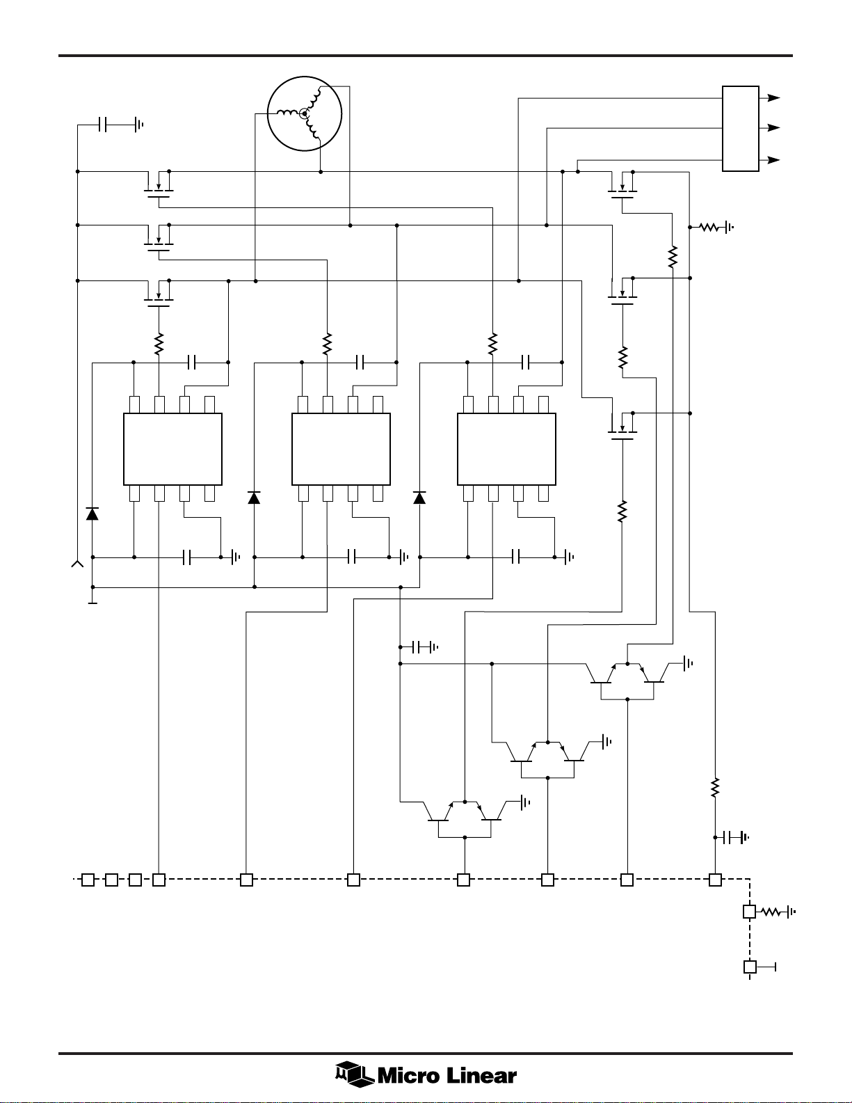
Figure 3. 3-Phase Motor Controller with INT-100 High Voltage Drivers
0.1µF
100kΩ
100kΩ
200kΩ
0.1µF
160kΩ
V
R
SPEED
V
0.1µF
V
REF
R
REF
SPEED
MIN
7
8
5
6
4
GND
12V
V
CC
26
8V REF
SPEED
CONTROLLER
C
GM1
2717
0.47µF
FREQ.
SINE
SINE
28
C
0.001µF0.001µF
12
GM2
C
0
A
B
SINE
A
10 13
AMPLITUDE
SINE
B
C
PWM
GENERATOR
PWM SINE
CONTROLLER
F/R
220pF
PWM
1811
COAST143PH/2PH
ML4423
UNDER VOLTAGE
LOCKOUT
OUTPUT
DRIVE & SHOOT
THROUGH
PROTECTION
CURRENT
LIMIT
5V/12V
SELECT
92515
R
166kΩ
A
99kΩ 49.5kΩ
99kΩ
2
3
1kΩ
+12V
1
H
L
0.15µF
IN
PWR
INT100
IN
4
5
15
1kΩ
11
12,13,14
8
7
SENSE
A
1
SENSE
C
2
SENSE
B
3
+12V
H A
24
L A
21
H B
22
L B
19
H C
23
L C
20
I
SENSE
16
DT
A
+12V
DRIVE
1kΩ
R
LIMIT
330pF 250mΩ
B
DRIVE
0.15µF
C
B
500Ω
0.30µF
+V
MOTOR
170–400V
10Ω
+
1µF
10Ω
C
100Ω
100Ω
Note: Use Extreme caution with high voltage AC motor control and drive circuitry.
When the motor is spinning at the desired speed, and the speed is rapidly reduced,
the energy stored in the rotation will generate a voltage greater than the +V
MOTOR
node,
HV POWER STAGE
and destruction of the power transistors, high side driver, ML4423
controller and the power supply may occur.
ML4423
7
Page 8
ML4423
+
330µF
170 – 360V
400V
IRF740IRF740IRF740
IR2118
MUR150
8
VB
CC
V
1
7
HO
IN
2
B
A
SENSE
A
AC MOTOR
FEEDBACK
NETWORK
B
SENSE
C
C
SENSE
IRF740
25V
1µF
22Ω
25V
1µF
22Ω
C21
25V
22Ω
1µF
LIMIT
22Ω
250mΩ R
22Ω
6
VS
COM
3
25V
5
N/C
N/C
4
1.0µF
IR2118
MUR150
8
VB
VCCIN
1
7
HO
2
25V
6
VS
COM
3
1.0µF
5
N/C
N/C
4
IR2118
MUR150
8
VB
VCCIN
1
7
HO
2
25V
6
VS
COM
3
1.0µF
5
N/C
N/C
4
IRF740 IRF740
22Ω
MOTOR
+V
+12V
1
A
SENSE
2
C
SENSE
3
B
SENSE
24
H A
22
H B
23
H C
+
ML4423
1.0µF
2N3904
21
L A
2N3906
19
L B
20
L C
1kΩ
16
SENSE
I
330pF
240kΩ
9
DT
R
25
5V/12V SELECT
+12V
Figure 4. ML4423 Output Stage Using IR2118 High Side Drivers
8
Page 9

ML4423
PHYSICAL DIMENSIONS
28
PIN 1 ID
1
0.180 MAX
(4.57 MAX)
0.125 - 0.135
(3.18 - 3.43)
inches (millimeters)
Package: P28N
28-Pin Narrow PDIP
1.355 - 1.365
(34.42 - 34.67)
0.045 - 0.055
(1.14 - 1.40)
0.015 - 0.021
(0.38 - 0.53)
0.100 BSC
(2.54 BSC)
SEATING PLANE
0.280 - 0.296
(7.11 - 7.52)
0.020 MIN
(0.51 MIN)
0.299 - 0.325
(7.60 - 8.26)
0º - 15º
0.008 - 0.012
(0.20 - 0.31)
0.024 - 0.034
(0.61 - 0.86)
(4 PLACES)
0.090 - 0.094
(2.28 - 2.39)
Package: S28
28-Pin SOIC
0.699 - 0.713
28
PIN 1 ID
1
(17.75 - 18.11)
0.050 BSC
(1.27 BSC)
0.012 - 0.020
(0.30 - 0.51)
0.291 - 0.301
(7.39 - 7.65)
0.095 - 0.107
(2.41 - 2.72)
SEATING PLANE
0.398 - 0.412
(10.11 - 10.47)
0.005 - 0.013
(0.13 - 0.33)
0º - 8º
0.022 - 0.042
(0.56 - 1.07)
0.009 - 0.013
(0.22 - 0.33)
9
Page 10

ML4423
ORDERING INFORMATION
PART NUMBER TEMPERATURE RANGE PACKAGE
ML4423CP (End Of Life) 0ºC to 70ºC 28-Pin Narrow PDIP (P28N)
ML4423CS (End Of Life) 0ºC to 70ºC 28-Pin SOIC (S28)
ML4423IP (End Of Life) –40ºC to 85ºC 28-Pin Narrow PDIP (P28N)
ML4423IS (End Of Life) –40ºC to 85ºC 28-Pin Narrow PDIP (P28N)
© Micro Linear 2000. is a registered trademark of Micro Linear Corporation. All other trademarks are the property of their
respective owners.
Products described herein may be covered by one or more of the following U.S. patents: 4,897,611; 4,964,026; 5,027,116;
5,281,862; 5,283,483; 5,418,502; 5,508,570; 5,510,727; 5,523,940; 5,546,017; 5,559,470; 5,565,761; 5,592,128; 5,594,376;
5,652,479; 5,661,427; 5,663,874; 5,672,959; 5,689,167; 5,714,897; 5,717,798; 5,742,151; 5,747,977; 5,754,012; 5,757,174;
5,767,653; 5,777,514; 5,793,168; 5,798,635; 5,804,950; 5,808,455; 5,811,999; 5,818,207; 5,818,669; 5,825,165; 5,825,223;
5,838,723; 5.844,378; 5,844,941. Japan: 2,598,946; 2,619,299; 2,704,176; 2,821,714. Other patents are pending.
2092 Concourse Drive
San Jose, CA 95131
Tel: (408) 433-5200
DS4423-01
10
Fax: (408) 432-0295
www.microlinear.com
4/21/98 Printed in U.S.A.
 Loading...