

Page 1
Sensorless Spindle Motor Controller
GENERAL DESCRIPTION
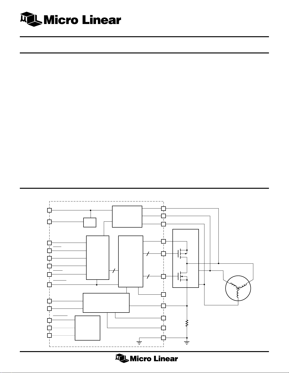
The ML4411 provides complete commutation for delta or
wye wound Brushless DC (BLDC) motors without the need
for signals from Hall Effect Sensors. This IC senses the
back EMF of the three motor windings (no neutral
required) to determine the proper commutation phase
angle using Phase Lock Loop techniques. This technique
will commutate virtually any 3-phase BLDC motor and is
insensitive to PWM noise and motor snubbing. The
ML4411 is architecturally similar to the ML4410 but with
improved braking and brown-out recovery circuitry.
Included in the ML4411 is the circuitry necessary for a
Hard Disk Drive microcontroller driven control loop.
The ML4411 controls motor current with either a constant
off-time PWM or linear current control driven by the
microcontroller. Braking and Power Fail are also included
in the ML4411.
The timing of the start-up sequencing is determined by the
micro, allowing the system to be optimized for a wide
range of motors and inertial loads.
May 1997
ML4411*/ML4411A**
The ML4411A includes a comparator on the P3 output to
prevent cross-conduction.
FEATURES
■ Back-EMF commutation provides maximum torque
for minimum “spin-up” time for spindle motors
■ Accurate, jitter-free phase locked motor speed
feedback output
■ Linear or PWM motor current control
■ Easy microcontroller interface for optimized start-up
sequencing and speed control
■ Power fail detect circuit with delayed braking
■ Drives external N-channel FETs and P-channel FETs
■ Back-EMF comparator detects motor rotation after
power fail for fast re-lock after brownout
The ML4411 modulates the gates of external N-Channel
power MOSFETs to regulate the motor current. The IC
drives P-Channel MOSFETs directly.
BLOCK DIAGRAM
RC
20
C
VCO
14
VCO/TACH OUT
15
RESET
16
I
RAMP
21
ENABLE E/A
18
BRAKE
26
DIS PWR
8
I
CMD
28
I
LIMIT
27
PWR FAIL
17
+5
19
VCC
25
VCO
LOGIC
AND
CONTROL
LINEAR OR PWM
CURRENT CONTROL
POWER
FAIL
DETECT
BACK-EMF
SAMPLER
GATE
DRIVE
6
* This Product Is Obsolete
** This Product Is End Of Life As Of August 1, 2000
PH1
22
PH2
23
PH3
24
POWER
DRIVERS
BLDC
MOTOR
PATENTED
3
3
VCC2
P1-3
N1-3
C
BRK
I
SENSE
C
C
OTA
GND
4
7
12
OS
13
6
1
1
Page 2
ML4411/ML4411A
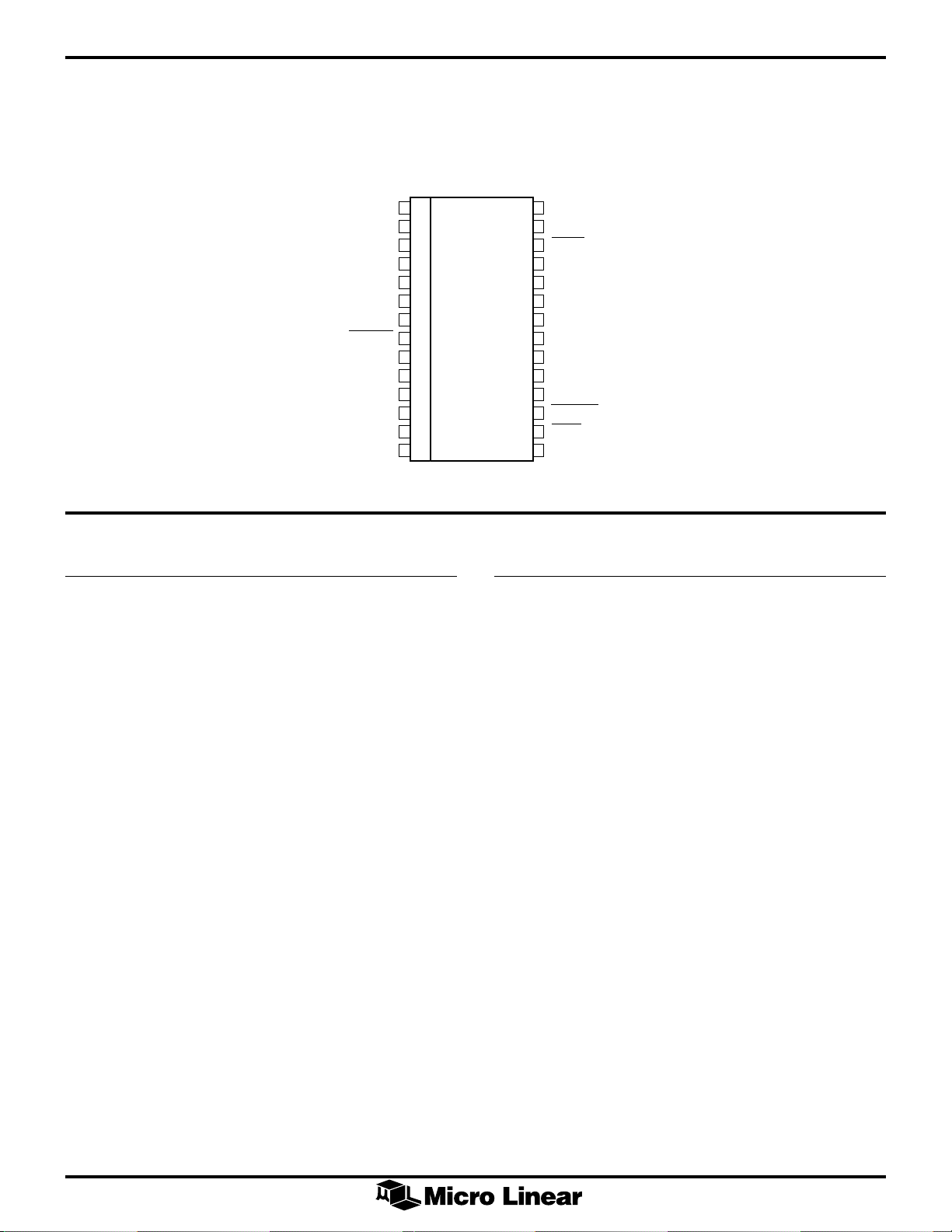
PIN CONFIGURATION
ML4411
28-Pin SOIC (S28W)
GND
VCC2
C
OTA
C
BRK
DIS PWR
N1
N2
N3
I
SENSE
C
C
VCO
1
P1
2
P2
3
4
P3
5
6
7
8
9
10
11
12
13
OS
14
TOP VIEW
I
28
I
27
BRAKE
26
VCC
25
PH3
24
PH2
23
PH1
22
I
21
RC
20
+5V
19
ENABLE E/A
18
PWR FAIL
17
RESET
16
VCO/TACH OUT
15
CMD
LIMIT
RAMP
PIN DESCRIPTION
PIN NAME FUNCTION PIN NAME FUNCTION
1 GND Signal and Power Ground
2 P1 Drives the external P-channel
transistor driving motor PH1
3 P2 Drives the external P-channel
transistor driving motor PH2
4V
CC2
12V power and power for the
braking function
5 P3 Drives the external P-channel
transistor driving motor PH3
6C
OTA
Compensation capacitor for linear
motor current amplifier loop
7C
BRK
Capacitor which stores energy to
charge N-channel MOSFETs for
braking with power off.
8 DIS PWR A logic 0 on this pin turns off the N
and P outputs and causes the TACH
comparator output to appear on TACH
OUT
9-11 N1, N2 N3 Drives the external N-channel
MOSFETs for PH1, PH2, PH3
12 I
13 C
SENSE
OS
Motor current sense input
Timing capacitor for fixed off-time
PWM current control
14 C
VCO
Timing capacitor for VCO
15 VCO/TACH Logic Output from VCO or TACH
OUT comparator
16 RESET Input which holds VCO off and sets the
IC to the RESET condition
17 PWR FAIL A “0” output indicates 5V or 12V is
under-voltage. This is an open
collector output with a 4.5ký pull-up
to +5V
18 ENABLE E/A A ”1” logic input enables the error
amplifier and closes the back-EMF
feedback loop
19 +5V 5V power supply input
20 RC VCO loop filter components
21 I
RAMP
Current into this pin sets the initial
acceleration rate of the VCO during
start-up
22 PH1 Motor Terminal 1
23 PH2 Motor Terminal 2
24 PH3 Motor Terminal 3
25 V
CC
12V power supply. Terminal which is
sensed for power fail
26 BRAKE A ”0” activates the braking circuit
27 I
LIMIT
Sets the threshold for the PWM
comparator
28 I
CMD
Current Command for Linear Current
amplifier
2
Page 3
ML4411/ML4411A
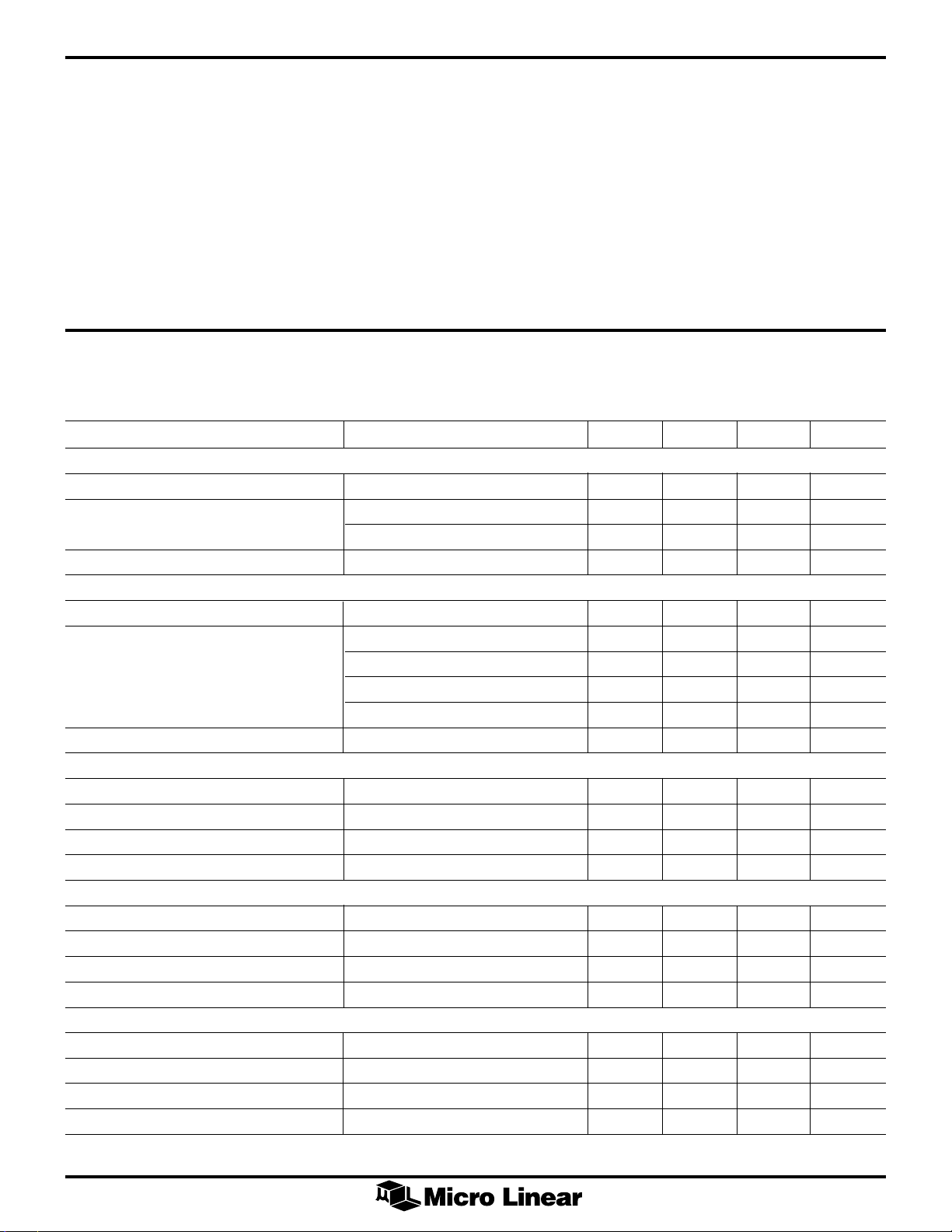
ABSOLUTE MAXIMUM RATINGS
Absolute maximum ratings are those values beyond which
the device could be permanently damaged. Absolute
maximum ratings are stress ratings only and functional
device operation is not implied.
Supply Voltage (pins 4, 25) ........................................ 14V
OPERATING CONDITIONS
Temperature Range ........................................0°C to 70°C
VCC Voltage +12V (pin 25) ........................... 12V ± 10%
+5V (pin 19) ................................................ 5V ± 10%
I(RAMP) current (Pin 21)................................. 0 to 100µA
I Control Voltage Range (pins 27, 28) ................ 0V to 7V
Output Current (pins 2, 3, 5, 9,10,11) .................±150mA
Logic Inputs (pins 16, 17, 18, 25) .................... –0.3 to 7V
Junction Temperature ............................................ 150°C
Storage Temperature Range ..................... –65°C to 150°C
Lead Temperature (Soldering 10 sec.) .................... 150°C
Thermal Resistance (qJA) ...................................... 60°C/W
ELECTRICAL CHARACTERISTICS
Unless otherwise specified, TA = Operating Temperature Range, V
C
= 0.02µF
OS
PARAMETER CONDITIONS MIN TYP MAX UNITS
Oscillator (VCO) Section (V
Frequency vs. V
Frequency V
Reset Voltage at C
Sampling Amplifier (Note 1)
V
RC
I
RC
V
PIN21
Motor Current Control Section
I
Gain V
SENSE
One Shot Off Time 12 25 33 µs
I
Transconductance Gain 0.19 mmho
CMD
I
, I
CMD
LIM
Power Fail Detection Circuit
12V Threshold 9.1 9.8 10.5 V
Hysteresis 150 mV
5V Threshold 3.8 4.25 4.5 V
Hysteresis 70 mV
Logic Inputs
Voltage High (VIH)2V
Voltage Low (VIL) 0.8 V
Current High (IIH)V
Current Low (IIL)V
PIN 20
VCO
Bias Current VIN = 0 0 –100 –400 nA
PIN16
= 5V)
1V - V
VCO
V
VCO
Mode = 0 125 250 mV
State R 125 250 mV
V
PIN18
V
PIN18
V
PIN18
V
PIN18
R
PIN21
PIN27
= 2.7V –10 1 10 µA
IN
= 0.4V –500 –350 –200 µA
IN
- 10V 300 Hz/V
PIN20
= 6V 1450 1800 2150 Hz
= 0.5V 70 140 210 Hz
= 0V, R
= 5V, State A, V
= 5V, State A, V
= 5V, State A, V
= 39ký to +5V 1.0 1.1 1.20 V
= 5V, 0V - V
RAMP
PIN28
= V
CC
= 39ký 70 100 130 µA
= 4V 30 50 90 µA
PH2
= 6V –13 2 13 µA
PH2
= 8V –30 –50 –90 µA
PH2
- 2.5V 4.5 5 5.5 V/V
= 12V, R
CC2
SENSE
= 1ý, C
OTA
= C
VCO
= 0.01µF,
3
Page 4
ML4411/ML4411A
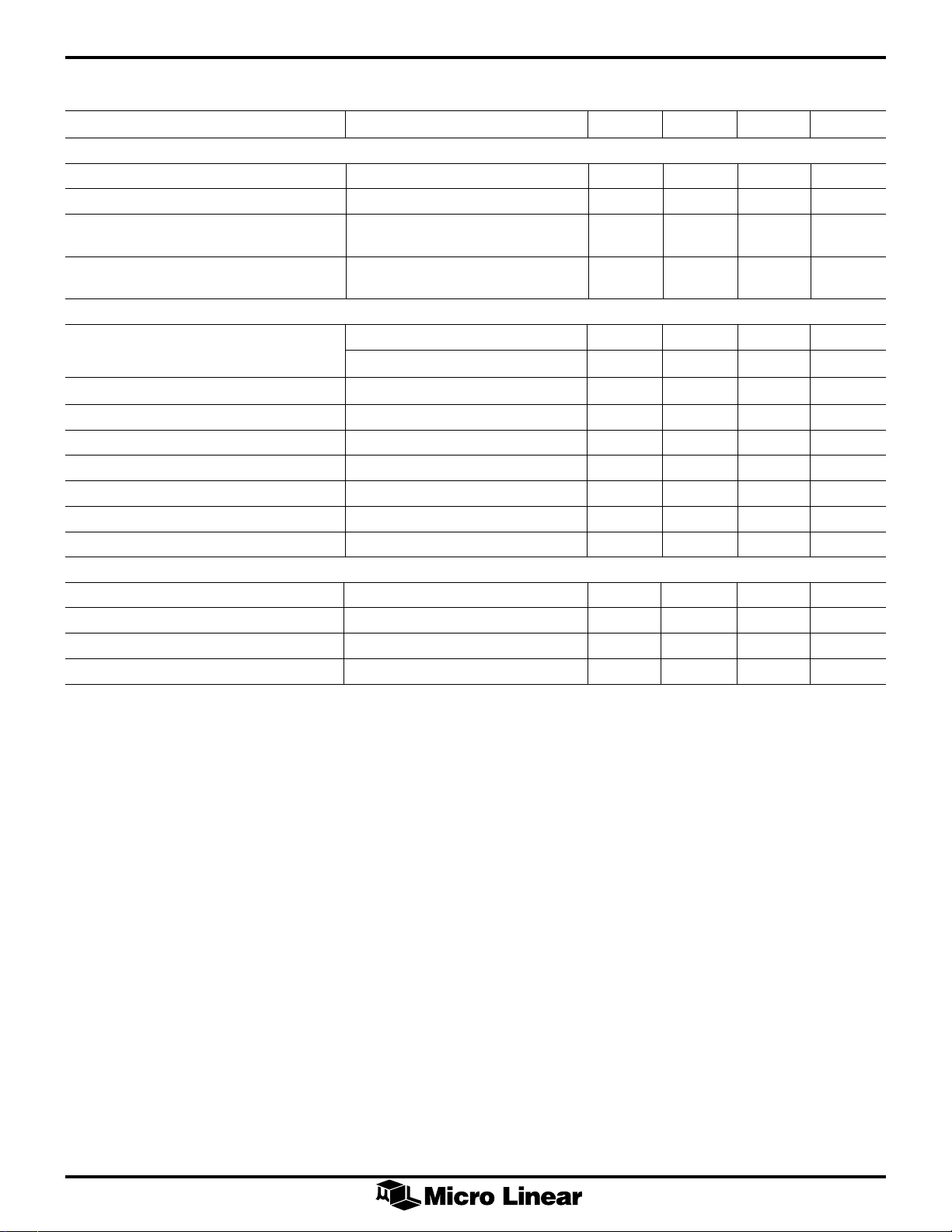
ELECTRICAL CHARACTERISTICS (Continued)
PARAMETER CONDITIONS MIN TYP MAX UNITS
Braking Circuit (V
Brake Active Threshold 0.8 1.2 1.6 V
PIN 26 Bias Current V
N-Channel Leakage V
Current VCC, V
C
BRK
Outputs (I
CMD
= I
IP Low VP = 0.8V 5 7 19.5 mA
VP High IP = –10µA VCC – 0.4 V
P3 Comparator Threshold V
VN High V
VN Low IN = 1mA 0.2 0.7 V
LOGIC Low (VOL)I
VCO/TACH V
OH
POWER FAIL V
Supply Currents (N and P Outputs Open)
5V Current 34mA
V
Current 38 50 mA
CC
V
Current ML4411 2 3 mA
CC2
V
Current ML4411A 2.6 3.75 mA
CC2
Note 1. For explanation of states, see Figure 5 and Table 1.
OH
PIN17
LIMIT
= 0V)
= 2.5V)
= 0V 0.3 1 µA
PIN26
, V
CC
V
PIN17
V
PIN7
V
= 0.4V 2 4 mA
P
PIN12
OUT
I
OUT
I
OUT
= 0V 0 0.06 10 nA
CC2
= 0V, VN = 4V
CC2
= 0V, V
= 3V 20 85 µA
PIN26
= 6V
= 0V V
– 1.6 V
CC2
– 3.2 10 VCC – 1.2 V
CC2
– 0.8 V
CC2
= 0.4mA 0.5 V
= –100µA 2.4 V
= –10µA V
PIN19
– 0.2 V
PIN19
– 0.1 V
PIN19
V
4
Page 5
FUNCTIONAL DESCRIPTION
ML4411/ML4411A
The ML4411 provides closed-loop commutation for
3-phase brushless motors. To accomplish this task, a VCO,
integrating Back-EMF Sampling error amplifier and
sequencer form a phase-locked loop, locking the VCO to
the back-EMF of the motor. The IC also contains circuitry
to control motor current with either linear or constant offtime PWM modes. Braking and power fail detection
functions are also provided on chip. The ML4411 is
designed to drive external power transistors (N-channel
sinking transistors and PNP sourcing transistors) directly.
Start-up sequencing and motor speed control are
accomplished by a microcontroller. Speed sensing is
accomplished by monitoring the output of the VCO,
which will be a signal which is phased-locked to the
commutation frequency of the motor.
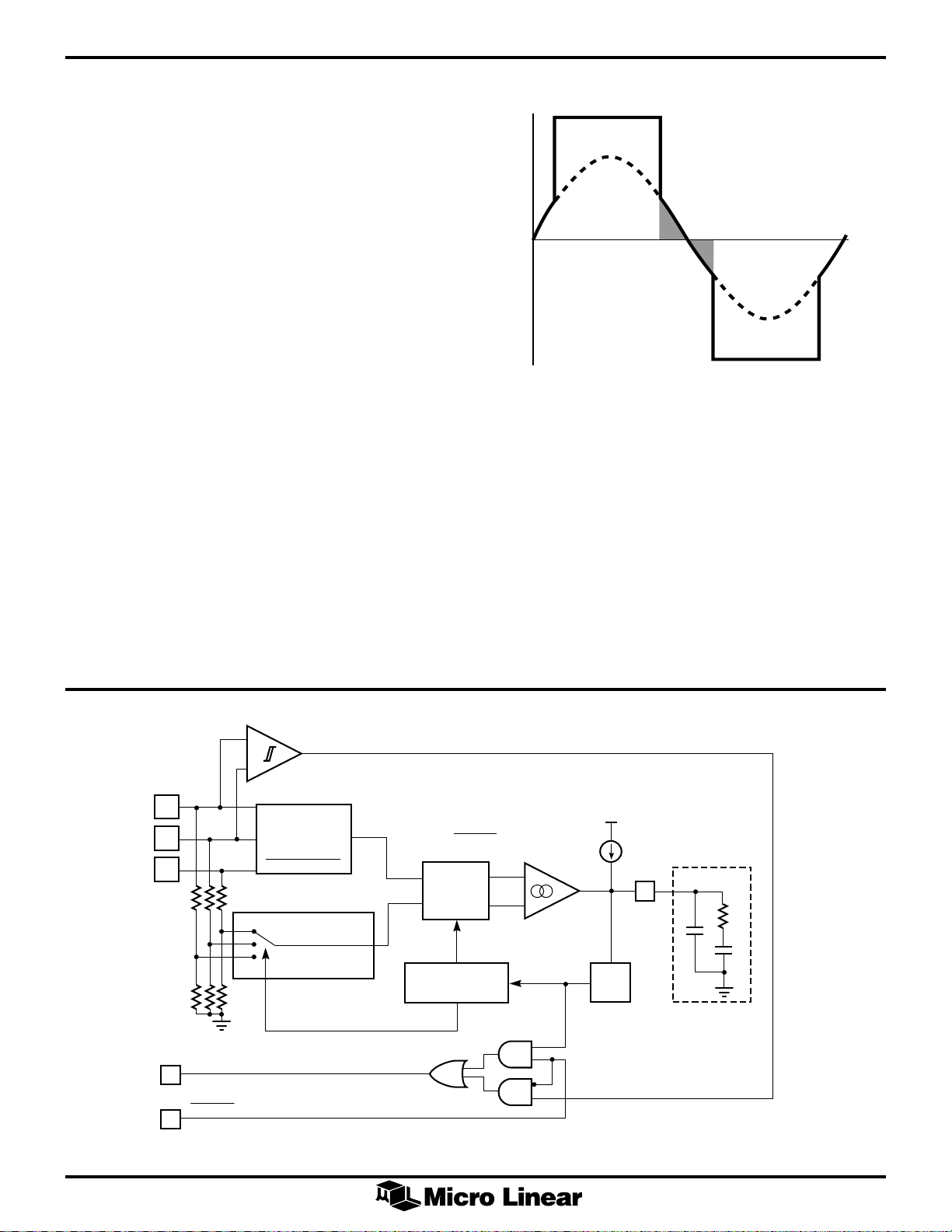
BACK-EMF SENSING AND COMMUTATOR
The ML4411 contains a patented back-EMF sensing
circuit which samples the phase which is not energized
(Shaded area in figure 2) to determine whether to increase
or decrease the commutator (VCO) frequency. A late
commutation causes the error amplifier to charge the
filter (RC) on pin 20, increasing the VCO input while
early
commutation causes pin 20 discharge. Analog speed
control loops can use pin 20 as a speed feedback voltage.
The input impedance of the three PH inputs is about 8Ký
to GND. When operating with a higher voltage motor, the
PH inputs should be divided down in voltage so that the
maximum voltage at any PH input does not exceed VCC.
NEUTRAL
0 60 120 180 240 0300
Figure 2. Typical motor phase waveform with Back-EMF
superimposed (Ideal Commutation)
VCO AND PHASE DETECTOR CALCULATIONS
The VCO should be set so that at the maximum frequency
of operation (the running speed of the motor) the VCO
control voltage will be no higher than VCC
– 1V. The
MIN
VCO maximum frequency will be:
F POLES RPM
=× ×005.
MAX
where POLES is the number of poles on the motor and
RPM is the maximum motor speed in Revolutions Per
ΦA
ΦB
ΦC
8K
8K
VCO /TACH OUT
DIS PWR
ROTATION
+
SENSE
–
NEUTRAL
SIMULATOR
ΦA + ΦB + ΦC
MULTIPLEXER
Va – Vb
=
I
RC
8K
6
SIGN
CHANGER
COMMUTATION
LOGIC
a
+
b
–
FIGURE 1. BACK EMKF sensing block diagram
+
I(PIN 21)
LOOP FILTER
RC
R
C1
C2
VCO
5
Page 6

Minute.
ML4411/ML4411A
The minimum VCO gain derived from the specification
table (using the minimum Fvco at V
−
×
VCO
6
= 9.5V, then
−
6
K
VCO MIN
()
242 10
=
Assuming that the V
××
95 242 10
C
VCO
..
=
.
C
VCO(MAX)
F
MAX
VCO
= 6V) is:
or
C
=
VCO
3000
2500
2000
1500
1000
FREQUENCY (Hz)
460
POLES RPM
×
F
µ
0.01µF
0.02µF
START-UP SEQUENCING
When the motor is initially at rest, it is generating no
back-EMF. Because a back-EMF signal is required for
closed loop commutation, the motor must be started
“open-loop” until a velocity sufficient to generate some
back-EMF is attained (around 100 RPM). The following
steps are a typical procedure for starting a motor which is
at rest.
Step 1: The IC is held in reset (state R) with full power
applied to the windings (see figure 6). This aligns the rotor
to a position which is 30° (electrical) before the center of
the first commutation state.
Step 2: Reset is released, and a fixed current is input to
pin 21 and appears as a current on pin 20, and will ramp
the VCO input voltage, accelerating the motor at a fixed
rate.
Step 3: When the motor speed reaches about 100 RPM,
the back EMF loop can be closed by pulling pin 18 high.
500
0
024681012
V
(VOLTS)
VCO
Figure 3. VCO Output Frequency vs. V
VCO
(Pin 20)
Figure 4 shows the transfer function of the Phase Lock
Loop with the phase detector formed from the sampled
phase through the Gm amplifier with the loop filtered
formed by R, C1, and C2.
The impedance of the loop filter is
Zs
SAMPLED
PHASE
RC
()
=
Csss
1
1
F
OUT
LEAD
ω
()
+
LAG
K
–4
VCO
VCO
Gm = 1.25 x 10
+
–
(HZ/V)
RC
Z
RC
R
C1
ω
()
+
Figure 4. Back EMF Phase Lock Loop Components
C2
RESET/
ALIGN
P1, P3, N2 ON
VCO FREQUENCY
0
RESET
ENABLE E/A
OPEN-LOOP
(STEPPING)
CLOSED LOOP
Figure 6. Typical Start-up Sequence.
Using this technique, some reverse rotation is possible.
The maximum amount of reverse rotation is 360/N, where
N is the number of poles. For an 8 pole motor, 45° reverse
rotation is possible.
For quick recovery following a momentary power failure,
the following steps can be taken:
PIN PIN PIN I
STEP 16 18 21 I
1 0 0 FIXED I
2 1 0 FIXED I
3110 I
LIMIT
CMD
MAX
MAX
MAX
Where the lead and lag frequencies are set by:
1
=
ω
ω
LEAD
LAG
RC
CC
+
12
=
RC C
2
12
6
Table 2. Start-up Sequence.
Page 7

ML4411/ML4411A
OUTPUTS INPUT
STATE N1 N2 N3 P1 P2 P3 SAMPLING
R OR 0 OFF ON OFF ON OFF ON N/A
A OFF OFF ON ON OFF OFF PH2
B OFF OFF ON OFF ON OFF PH1
C ON OFF OFF OFF ON OFF PH3
D ON OFF OFF OFF OFF ON PH2
E OFF ON OFF OFF OFF ON PH1
F OFF ON OFF ON OFF OFF PH3
Table 1. Commutation States.
RESET
4.3 V
C
VCO
2.3 V
VCO OUT
STATE
R
0A BC D E F A
Figure 5. Commutation Timing and Sequencing.
Step 1a: The IC is held in reset (state R) with I
CMD
low
and DIS PWR low. The Micro Processor monitors the VCO/
TACH OUT pin to determine if a signal is present. If a
signal is present, the frequency is determined (by
measuring the period). If a signal is not present, proceed
to the routine described above for starting a motor which
is a rest.
Step 2a: Release RESET and DIS PWR. Apply a current to
pin 21 and monitor the VCO/TACH OUT pin for VCO
frequency.
Step 3a: When the VCO frequency approaches 6 X the
motor frequency (or where the motor frequency has
decelerated to by coasting during the time the VCO
frequency was ramping up) the back EMF loop can be
closed by pulling pin 18 high and motor current brought
up with I
CMD
or I
LIMIT
.
ADJUSTING OPEN LOOP STEP RATE
I
should be set so that the VCO’s frequency ramp
RAMP
during “open loop stepping” phase of motor starting is less
than the motor’s acceleration rate. In other words, the
motor must be able to keep up with the VCO’s ramp rate
in open loop stepping mode. The VCO’s input voltage
(V
) ramp rate is given by:
PIN 20
dV
VCO RAMP
dt
I
≈
CC
12
+
since
FKV
=×
VCO VCO VCO
−
6
×
K
VCO MAX
()
then combining the 3 equations I
410
=
C
VCO
can be calculated
RAMP
from the desired maximum open loop stepping rate the
motor can follow.
I
RAMP
dF
VCO VCO
<
dt
CCC
()
×+
12
6
−
410
×
7
Page 8

ML4411/ML4411A
The motor will start more consistently and tolerate a wider
variation in open loop step rate if there is some damping
on the motor (such as head drag) during the open loop
modes.
The tolerance of the open loop step VCO acceleration
C2, and C
dF
VCO
depends on the tolerances of K
dt
. For more optimum spin up times, these
VCO
VCO
, I
RAMP
, C1,
variables can be digitally “calibrated” out by the
microprocessor using the following procedure:
1. Reset the IC by holding pin 16 low for at least 5µs.
2. Go into open loop step mode with no current on
the motor and measure the difference between the
first two complete VCO periods with the PWM
signal at 50% duty cycle:
ENABLE E/A = (see below)
I
= 0V
CMD
PWM OUT = 50%
MicroP ML4411
PWM OUT
IN
I(RAMP)
VCO/TACH OUT
Figure 7. Auto-Calibration of Open-Loop Step
Rate.
3. Compute a correction factor to adjust I
RAMP
current
by changing the PWM duty cycle from the
Micro (D.C.)
F DESIRED
()
∆
DC NEW
..( ) %
=×50
VCO
F MEASURED
()
∆
VCO
4. Use new computed duty cycle for open loop
stepping mode and proceed with a normal start-up
sequence.
If this auto calibration is used ENABLE E/A can be tied
permanently high, eliminating a line from the Micro.
Since there is offset associated with the Phase Detector
Error Amp (E/A), more current than is being injected by
I
may be taken out of pin 20 if the offset is positive
RAMP
(into pin 20) if the error amp were enabled during the
open loop stepping mode. In that case, V
would not
VCO
rise and the motor would not step properly. The effect of
E/A offset can also be canceled out by the auto calibration
algorithm described above allowing the E/A to be
permanently enabled.
PWM AND LINEAR CURRENT CONTROL
To facilitate speed control, the ML4411 includes two
current control loops — linear and PWM (figure 9). The
linear control loop senses the motor current on the I
terminal through R
. An internal current sense
SENSE
SENSE
amplifier’s (A2) output modulates the gates of the 3 Nchannel MOSFET’s when OTA OUT is tied to OTA IN, or
can modulate a single MOSFET gate tied to OTA OUT.
When operated in this mode, OTA IN is tied to 12V, and
N1-N3 are saturated switches. This method produces the
lowest current ripple at the expense of an extra MOSFET.
The linear current control modulates the gates of the
external MOSFET drivers. Amplifier A2 is a
transconductance amplifier which amplifies the difference
between I
CMD
and I
. The transconductance gain of
SENSE
A2 is:
ý
−
g
=×
1 875 10
.
m
The current loop is compensated by C
4
which forms a
OTA
pole given by
P
C
OTA
−
4
×
9 375 10
.
=
ω
This time constant should be fast enough so that the
current loop settles in less than 10% of T
highest motor speed to avoid torque ripple to V
VCO
at the
TH
mismatch of the N-Channel MOSFETs.
The I
input pin should be kept below 1V. If I
SENSE
SENSE
goes above 1V, a bias current of about –300µA will flow
out of pin 12 and the N outputs will be inhibited. Bringing
I
below 0.7V removes the bias current to its normal
SENSE
level. For this reason, the noise filter resistor on the I
SENSE
pin (1Ký on Figure 10) should be less than 1.5Ký.
The noise filter time constant should be great enough to
filter the leading edge current spike when the N-FETs turn
on but small enough to avoid excessive phase shift in the
I
signal.
SENSE
OUTPUT DRIVERS
The motor’s source drivers (P1 thru P3) are open-collector
NPN’s with internal 16Ký pull-up resistors. N3is inhibited
until P3 is within 1.4V (typ) of V
on the ML4411A.
CC2
Drivers N1 through N3 are totem-pole outputs capable of
sourcing and sinking 10mA. Switching noise in the
external MOSFETs can be reduced by adding resistance in
series with the gates.
V
sC
OTA
−
4
×
1 875 10
.
A
=
8
Page 9

BRAKING
As shown in figure 9, the braking circuit pulls the N-
Channel MOSFET gates high when BRAKE falls below a
1.4V threshold. After a power failure, C
slowly through R
providing a delay for retract to occur
DLY
is discharged
DLY
before the braking circuit is activated. The N-Channel
buffer (B1) tri-states when the BRAKE pin reaches 2.1V to
ensure that no charge from C
is lost through the pull-
BRK
down transistor in B1. To brake the motor with external
signals, first disable power by pulling pin 8 low, then pull
pin 26 below 1.4V using an open drain (or diode isolated)
output.
The bias current for the Braking circuits comes from
VCC2. When the N-Channel MOSFETs turn on, no
additional power is generated for VCC2 (motor back-EMF
rectified through out the MOSFET body diodes). After
VCC2 drops below 4V, Q2 turns off. Continued braking
relies on the CGS of the N-Channel MOSFETs to sustain
the MOSFET gate enhancement voltage.
ML4411/ML4411A
60
50
40
(µs)
30
OFF
T
20
10
0
0 0.01 0.02 0.03 0.04 0.05
C
OS
Figure 8. I
Output Off-Time vs. COS.
LIMIT
VCC2
16K
POWER FAIL
17 +5
R
C
DLY
DLY
26
8
27
28
12
4.5K
COMM. LOGIC
BRAKE
1.4V
DIS PWR
I
LIMIT
I
CMD
I
SENSE
DIS PWR
+
–
A
= 5
V
A1
VCC2 – 3V
UVLO
VCC2
2.1V
A4
COMMUTATION
UVLO
+
–
+
–
VCC2
+
A5
–
LOGIC
A3
+
–
1K
A6
P3 ONLY
A2
Q
ONE
SHOT
Q2
VCC
VCC2
TRI-
ST.
B1
VIN
C
BRK
P1 . . . P3
Q1
N1 . . . N3
7
R
SENSE
C
OS
13
VCC
C
OTA
6
Figure 9. Current Control, Output Drive and Braking Circuits.
9
Page 10

ML4411/ML4411A
APPLICATIONS
Figure 10 shows a typical application of the ML4411 in a
hard disk drive spindle control. Although the timing
necessary to start the motor in most applications would be
generated by a microcontroller, Fig. 11 shows a simple
“one shot” start-up timing approach.
Speed control can be accomplished either by:
1. Sensing the VCO OUT frequency with a
Microcontroller and adjusting I
via an analog
CMD
output form the Micro (PWM DAC).
2. Using analog circuitry for speed control. (Fig. 12).
1N5819
+12V
10
0.1
Q1
TO VCC
OUTPUT STAGE HINTS
In the circuit in Figure 10, Q1, Q2, and Q3 are IRFR9024
or equivalent. Q4, Q5, and Q6 are IRFR024 or equivalent.
New MOSFET packaging technology such as the Little
Foot series may decrease the PC board space. These
packages, however have much lower thermal inertia and
dissipation capabilities than the larger packages, and care
should be taken not to exceed their rated current and
junction temperature.
Since the output section in a full bridge application
consists of three half-H switches, cross-conduction can
occur. Cross-conduction is the condition where an N-FET
and P-FET in the same phase of the bridge conduct
simultaneously. This could happen under two conditions
(see figure 13):
VCC2
0.110
1K 1K 1K
Q2
Q3
510
510
100pF
0.02
+12
0.01
0.01
0.22
1
2
3
4
5
6
7
8
9
10
11
12
13
14
Q4
GND
P1
P2
VCC2
P3
C
OTA
C
BRK
DIS PWR
N1
N2
N3
I
SENSE
C
OS
C
VCO
I
CMD
I
LIMIT
BRAKE
VCC
PH3
PH2
PH1
I
RAMP
+5V
ENABLE E/A
PWR FAIL
RESET
VCO/TACH OUT
RC
Q5
Q6
510
5K
+5
28
27
26
25
24
23
22
21
20
19
18
17
16
15
1M
+12
+5
I
COMMAND
0.22
+5
510K
0.5
5K
ENABLE ERROR AMP
RESET (FROM MICRO)
POWER FAIL TO MICRO
VCO OUT
DISABLE POWER
10
Figure 10. ML4411 Typical Application
Page 11

ML4411/ML4411A
ML4411
PIN 17
TO ML4411
PIN 20
SYMBOL VALUE
A1 LM358
IC1 74HC14
D1, D2 IN4148
R1 1Mý
R2 1Mý
R3 100Ký
+5V
R1
1/6
D1
C1
IC1
R2
D2
C2
Figure 11. Analog Start-up Circuit
–
A1
+
R3
+12V
R5
R6
C3
R4
–
A1
+
SYMBOL VALUE
R4 100Ký
R5 50Ký
R6 50Ký
C1 3.3µF
C2 3.3µF
C3 0.47µF
1/6
IC1
1/6
IC1
TO ML4411
PIN 16
TO ML4411
PIN 18
TO ML4411
PIN 28
VCC2
1K
P
INHIBIT N3
–
A6
+
ML4411A ONLY
16K
P3
Q2
4
5
Figure 13. Alternate cross-conduction prevention for
ML4411A
In Condition 2 above, the P-Channel MOSFET is pulled up
inside the ML4411 with a 16Ký resistor. If the current
through C(CGp) is greater than VTH Þ 16K when the
N-FET turns on, the P-FET could turn on simultaneously,
causing cross-conduction. Adding R1 as shown in Figure
14 eliminates this. The size of R1 will depend on the fall
time of the phase voltage, and the size of the C(DGp). D1
may be needed for high power applications to limit the
negative current pulled (through C(DGn)) out of the
substrate diode in the ML4411 when P-FET turns off.
VCC2
R1
RG(P)
C(DGp)
C(DGn)
RG(N)
D1
P
N
Figure 14. Causes of Cross-conduction
Figure 12. Analog Speed Control
1. When transitioning from mode 0 to mode A (see table
1) P3 goes from on to off at the same time N3 goes
from off to on. If the P3 turns off slowly and N3 turns
on quickly, cross-conduction may occur. This condition
has been prevented inside the IC on the ML4411A
through the addition of comparator A6 on the P3
output (Figure 9). This comparator may cause an
oscillation when the N3 switches on due to the
capacitive coupling effect described below pulling the
P3 pin below VCC2-1.4V. To avoid this, use the circuit
in Figure 13.
2. When the MOSFET in the same phase switches on gate
current flows due to capacitive coupling of current
through the MOSFET’s drain to gate capacitance. This
could cause the device that was off to be turned on.
Adding a series damping resistor to the N-FET gate (RGn)
will slow the fall time. The damping resistor should be
low enough to:
Avoid turning on the N-Channel gate when the PNP
turns on via the same mechanism outlined in condition
2 above
Not severely increase the switching losses in the N-FET
UNIPOLAR OPERATION
Unipolar mode offers the potential advantage of lower
motor drive cost by only requiring the use of 3 transistors
to drive the motor. The ML4411 will operate in unipolar
mode (Figure 15) provided the following precautions are
taken:
1. The IC supplies should not exceed 12V + 10%.
2. The phase pins on the IC should not exceed the
supply voltage.
11
Page 12

ML4411/ML4411A
10K
10K 10K
+V
1
2
3
4
5
6
7
8
9
10
11
12
13
14
0.01
+V
0.5Ω
1.2K
+12
+5
0.02
0.01
+12
Figure 15. ML4411 Unipolar Drive Application
In unipolar operation, the motor‘s windings must be
allowed to drive freely to:
V
F(MAX)
= V
SUPPLY (MAX)
+ V
EMF (MAX)
Therefore, there can be no diodes to clamp the inductive
energy to V
. This energy must be clamped,
SUPPLY
however, to avoid an over-voltage condition on the
MOSFETs and other components. Typically, a V
CLAMP
voltage is created to provide the clamping voltage. The
inductive energy may either be dissipated (Figure 16) or
alternately efficiently regenerated back to the system
supply (Figure 17).
The circuit in Figure 15 is designed to minimize the
external components necessary, at some compromise to
performance. The 3 resistors from the motor phase
windings to the PH inputs work with the ML4411‘s 8Ký
internal resistance to ground to divide the motor‘s
phase voltage down, providing input signals that do not
exceed 12V.
V
= +24V
12V
BATTERY
CLAMP
C1
0.1
+12V
5V
REG
12V
LDO
10
+12V TO
VCC AND VCC2
+5V
0.1
0.11000
3.3K
+12
2.2
+5
+5
+12
+5
+
–
1M
+5
1M
C
DLY
GND
P1
P2
VCC2
P3
C
OTA
C
BRK
DIS PWR
N1
N2
N3
I
SENSE
C
OS
C
VCO
I
CMD
I
LIMIT
BRAKE
VCC
PH3
PH2
PH1
I
RAMP
+5V
ENABLE E/A
PWR FAIL
RESET
VCO/TACH OUT
RC
28
27
26
25
24
23
22
21
20
19
18
17
16
15
This circuit uses analog speed regulation. The 1Mý
resistor from Pin 20 to the speed regulation op amp
provides the function of injecting current into the VCO
loop filter for the open loop stepping phase of start-up
operation. The “one shot” circuitry to time the reset is
replaced by a diode and RC delay from the rising edge or
the POWERFAIL signal. The error amplifier is left enabled
continuously since at low speeds its current contribution
is negligible. The current injected into the loop filter must
be greater than the leakage current from the phase
detector amplifier for the motor to start reliably.
V
= +24V
CLAMP
50% DUTY
CYCLE
12V
BATTERY
L1
D1
0.1
Figure 17. Non-Dissipative Clamping Technique
10K
5V
REG
12V
LDO
12
Figure 16. Dissipative Clamping Technique
Page 13

ML4411/ML4411A
HIGHER VOLTAGE MOTOR DRIVE
To drive a higher voltage motor, the same precautions
regarding ML4411 voltage limitations as were outlined for
Unipolar drive above should be followed. Figures 14–16
provide several methods of translating the ML4411‘s P
outputs to drive a higher voltage.
+V
Q1
Q3
PML4411
+12V
Figure 18. High Voltage Translation using PNP Power
Transistor
+V
Q2
Q1
Q3
PML4411
+12V
Figure 19. High Voltage Translation using “Composite”
PNP Power Transistor
+V
Q2
Q1
PML4411
Q3
Figure 20. High Voltage Translation with NPN
Darlington
13
Page 14

ML4411/ML4411A
PHYSICAL DIMENSIONS inches (millimeters)
Package: S28
28-Pin SOIC
0.699 - 0.713
28
(17.75 - 18.11)
0.024 - 0.034
(0.61 - 0.86)
(4 PLACES)
0.090 - 0.094
(2.28 - 2.39)
0.291 - 0.301
(7.39 - 7.65)
PIN 1 ID
1
0.050 BSC
(1.27 BSC)
0.012 - 0.020
(0.30 - 0.51)
0.095 - 0.107
(2.41 - 2.72)
SEATING PLANE
0.398 - 0.412
(10.11 - 10.47)
0.005 - 0.013
(0.13 - 0.33)
0º - 8º
0.022 - 0.042
(0.56 - 1.07)
0.009 - 0.013
(0.22 - 0.33)
ORDERING INFORMATION
PART NUMBER TEMPERATURE RANGE PACKAGE
ML4411CS (Obsolete) 0°C to 70°C 28-Pin Wide SOIC (S28W)
ML4411ACS (End Of Life) 0°C to 70°C 28-Pin Wide SOIC (S28W)
© Micro Linear 1997 is a registered trademark of Micro Linear Corporation
Products described in this document may be covered by one or more of the following patents, U.S.: 4,897,611; 4,964,026; 5,027,116; 5,281,862; 5,283,483; 5,418,502; 5,508,570; 5,510,727; 5,523,940;
5,546,017; 5,559,470; 5,565,761; 5,592,128; 5,594,376; Japan: 2598946; 2619299. Other patents are pending.
Micro Linear reserves the right to make changes to any product herein to improve reliability, function or design.
Micro Linear does not assume any liability arising out of the application or use of any product described herein,
neither does it convey any license under its patent right nor the rights of others. The circuits contained in this
data sheet are offered as possible applications only. Micro Linear makes no warranties or representations as to
whether the illustrated circuits infringe any intellectual property rights of others, and will accept no responsibility
or liability for use of any application herein. The customer is urged to consult with appropriate legal counsel
before deciding on a particular application.
14
2092 Concourse Drive
San Jose, CA 95131
Tel: 408/433-5200
Fax: 408/432-0295
DS4411-01
 Loading...