

Page 1
PRELIMINARY
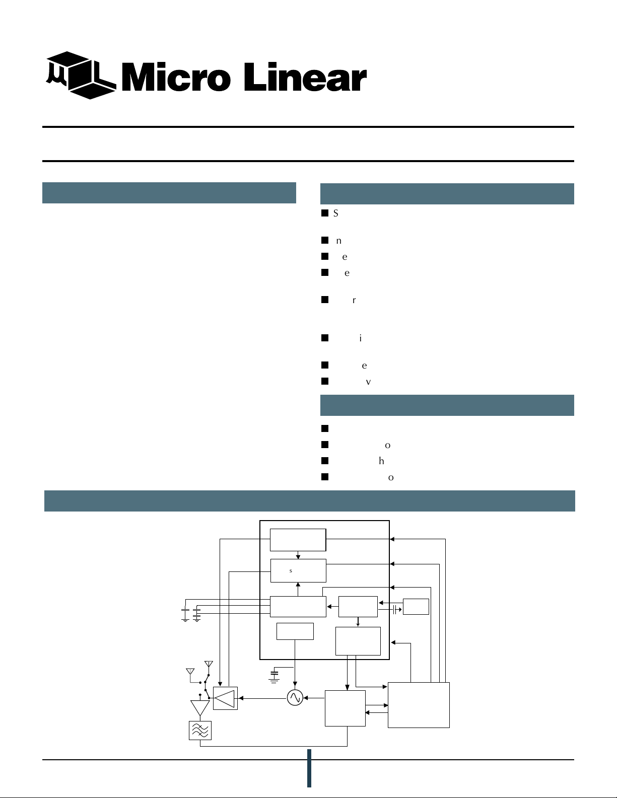
ML2731 PA Bias Controller
GENERAL DESCRIPTION
The ML2731 is a power amplifier (PA) bias controller with
support circuits for a typical radio transceiver. The IC
integrates a PA bias controller, a PA DC switch, a crystal
oscillator circuit, a negative voltage generator and two
voltage regulators. It can be used with GaAs FETs and
silicon bipolar devices.
Micro Linear’s ML2731, along with the ML2712 and the
ML2713, form a complete transceiver solution for the 2.4
GHz IEEE802.11 communication standard, as well as
other wireless ISM communication products.
In addition to supporting Micro Linear’s transceiver chip
set, the ML2731 can stand alone as:
A compact bias voltage controller
A compact negative voltage generator
A compact crystal oscillator
FEATURES
n
Sets PA current and power output using a bias control
loop
n
Integrates a PA DC supply switch
n
Prevents PA power-on if negative voltage is not present
n
Integrates all circuits needed for supporting a crystal
oscillator with 10MHz to 40MHz frequency range
n
Incorporates a fast starting, high switching frequency,
negative voltage generator requiring only small
ceramic capacitors
n
Contains voltage regulators for an oscillator, a negative
voltage generator and a 50mA 3.0V LDO output
n
Requires less than 1mA of current when powered down
n
Supply voltage ranges from 3.3V to 5.5V
APPLICATIONS
n
Cellular and Cordless Radios
n
WLAN Radios
n
Radios with GaAs FET Power Amplifiers
n
Fixed and Mobile radio transceivers
SIMPLIFIED BLOCK DIAGRAM
VPA
VBIAS
VNEG
GaAs FET Power Amplifier
PRELIMINARY DATASHEET
C1
C2
PA on/off switch
and current sense
Bias Control
Negative voltage
generator
Voltage
Regulator
REGO
ML2731
Crystal
Oscillator
Sine & square
wave drivers
CLKO
SINO
ML2712
ML2713
Radio
January, 2000
PAEN
ICON
NEGEN
XIN
Crystal
XOUT
PDN
Baseband Controller
(e.g. MSM7730B)
Page 2

PRELIMINARY
ML2731
TABLE OF CONTENTS
General Description ................................................................................................................................................... 1
Simplified Block Diagram .......................................................................................................................................... 1
Features...................................................................................................................................................................... 1
Applications ............................................................................................................................................................... 1
Block Diagram ........................................................................................................................................................... 3
Pin Configuration ....................................................................................................................................................... 4
Pin Descriptions ......................................................................................................................................................... 4
Functional Description ............................................................................................................................................... 6
Introduction.............................................................................................................................................................. 6
External Interfaces ................................................................................................................................................... 6
Mode Control ........................................................................................................................................................... 6
Description Of Operation ........................................................................................................................................... 6
Crystal Oscillator ..................................................................................................................................................... 7
Negative Voltage Generator ..................................................................................................................................... 7
Absolute Maximum Ratings........................................................................................................................................ 11
Electrical Tables ......................................................................................................................................................... 11
Electrical Characteristics............................................................................................................................................ 11
Operating Conditions ................................................................................................................................................. 11
Physical Dimensions .................................................................................................................................................. 12
Ordering Information .................................................................................................................................................. 12
WARRANTY
Micro Linear makes no representations or warranties with respect to the accuracy, utility, or completeness
of the contents of this publication and reserves the right to make changes to specifications and product
descriptions at any time without notice. No license, express or implied, by estoppel or otherwise, to any
patents or other intellectual property rights is granted by this document. The circuits contained in this
document are offered as possible applications only. Particular uses or applications may invalidate some of
the specifications and/or product descriptions contained herein. The customer is urged to perform its own
engineering review before deciding on a particular application. Micro Linear assumes no liability
whatsoever, and disclaims any express or implied warranty, relating to sale and/or use of Micro Linear
products including liability or warranties relating to merchantability, fitness for a particular purpose, or
infringement of any intellectual property right. Micro Linear products are not designed for use in medical,
life saving, or life sustaining applications.
© 2000. Micro Linear is a registered trademark of Micro Linear Corporation. All other trademarks are the property of their
respective owners.
Products described herein may be covered by one or more of the following U.S. patents: 4,897,611; 4,964,026; 5,027,116;
5,281,862; 5,283,483; 5,418,502; 5,508,570; 5,510,727; 5,523,940; 5,546,017; 5,559,470; 5,565,761; 5,592,128; 5,594,376;
5,652,479; 5,661,427; 5,663,874; 5,672,959; 5,689,167; 5,714,897; 5,717,798; 5,742,151; 5,747,977; 5,754,012; 5,757,174;
5,767,653; 5,777,514; 5,793,168; 5,798,635; 5,804,950; 5,808,455; 5,811,999; 5,818,207; 5,818,669; 5,825,165; 5,825,223;
5,838,723; 5.844,378; 5,844,941. Japan: 2,598,946; 2,619,299; 2,704,176; 2,821,714. Other patents are pending.
2
PRELIMINARY DATASHEET
January, 2000
Page 3
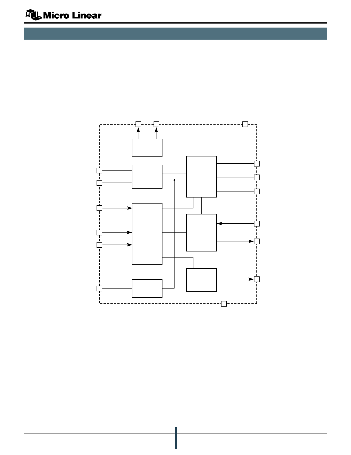
BLOCK DIAGRAM
PRELIMINARY
ML2731
XIN
XOUT
PAEN
NEGEN
PDN
REGO
SINO
15
16
6
7
14
3
CLKO
1 8
BUFFER
AND
DRIVERS
OSCILLATOR
AND
DIVIDER
REFERENCE
GENERATOR
AND
LOGIC
REGULATOR
NEGATIVE
VOLTAGE
GENERATOR
BIAS
CONTROL
SWITCH
AND
CURRENT
SENSE
VCC
2
10
VNEG
12
C1
11
C2
5
ICON
4
VBIAS
13
VPA
January, 2000
9
GND
PRELIMINARY DATASHEET
3
Page 4
PRELIMINARY
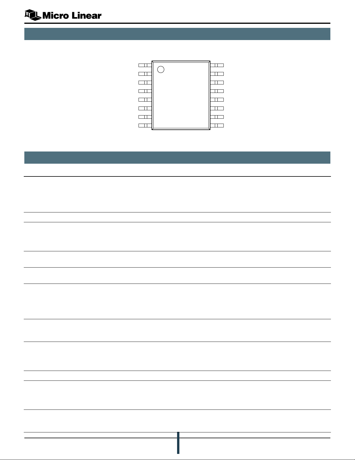
PIN CONFIGURATION
ML2731
16-Pin TSSOP (T16)
SINO
VCC
REGO
VBIAS
ICON
PAEN
NEGEN
CLKO
PIN DESCRIPTIONS
Pin # Signal Name I/O Description
1 SINO O (ANLG) Sine wave output. This pin is a low impedance output capable of
2 VCC O (ANLG) DC power supply
1
2
3
4
5
6
7
8
TOP VIEW
16
15
14
13
12
11
10
9
XOUT
XIN
PDN
VPA
C1
C2
VNEG
GND
driving a 2kW load. The signal is sourced with either a crystal
interfaced with on-chip components through XOIN (pin 15) and XOUT
(pin 16) or with a completely external oscillator through pin 15.
Taking PDN (pin 14) high switches off output
ML2731
3 REGO O (ANLG) IC regulator output. This is the output from the on IC regulator. It is
disabled in the SLEEP mode of operation and enabled in all other
modes. The nominal output voltage is 2.9 V and it has a low
impedance output which can source up to 50mA
4 VBIAS O (ANLG) PA bias voltage output. This output has limited drive capability of 3mA
and is intended to drive the gate or bias of the PA
5 ICON I (ANLG) Reference current input. Used by the PA bias control loop to set the PA
current level. This input appears as a virtual ground
6 PAEN I (CMOS) PA Enable. Transitions from high to low on this pin activate the PA
current ramp up function, switch the PA voltage supply switch on and
enable the PA bias control loop. Transitions from low to high activate
the PA current ramp down function and switch the PA voltage supply
off
7 NEGEN I (CMOS) Negative Voltage Enable. In conjunction with PDN and PAEN, NEGEN
controls the operational mode of the IC and enables the negative
voltage generator circuits
8 CLKO I (CMOS) Clock output. The frequency is set with either a crystal interfaced with
on-chip components through XOIN (pin 15) and XOUT (pin 16) or with
a completely external oscillator through pin 15. CLKO switches off
when device goes into SLEEP mode when PDN is taken high
9 GND GND Ground
10 VNEG O (ANLG) Negative regulator output. This pin is one of the outputs of the negative
switching regulator. A capacitor connected serves as a current
reservoir. Typically a 100nF capacitor is connected between pin 10
and GND
11 C2 O (ANLG) Noise Shunt. Negative voltage generator capacitor connection. This
output of the negative switching regulator shunts regulator noise to
ground using a 100nF bypass capacitor
4
PRELIMINARY DATASHEET
January, 2000
Page 5

PRELIMINARY
ML2731
PIN DESCRIPTIONS (continued)
Pin # Signal Name I/O Description
12 C1 O (ANLG) Noise Shunt. Negative voltage generator bypass capacitor connection.
Typically a 100nF capacitor is connected between pin C1 and C2
13 VPA O (ANLG) PA supply. This is the positive supply for the PA. It is switched by PAEN
in conjunction with PDN and NEGEN
14 PDN I (ANLG) Power down control. Disables all circuits and reduces power
consumption to less than 1mA
15 XIN I (ANLG) Crystal or oscillator input. This high input impedance is connected to
either an oscillator circuit or to a crystal
16 XOUT I (ANLG) Crystal-tank connection. This low impedance output drives the crystal
tank circuit
January, 2000
PRELIMINARY DATASHEET
5
Page 6

PRELIMINARY
FUNCTIONAL DESCRIPTION
ML2731
INTRODUCTION
EXTERNAL INTERFACES
The ML2731 has 3 logic inputs: PAEN, NEGEN and PDN.
These control lines are used to select the mode of
operation to be either SLEEP, STANDBY, PRETX or
TRANSMIT. (See Table 1)
NDPNEGENNEAPedoM
1XX PEELS
01X YBDNATS
001 XTERP
000 TIMSNART
Table 1. Circuit Enable Logic
MODE CONTROL
Mode Functions
The function of the ML2731 in each mode of operation:
DESCRIPTION OF OPERATION
Voltage Regulator
The ML2731 integrates two low noise voltage regulators.
The first regulator internally powers the crystal oscillator
support circuit, negative voltage generator support circuit
and other on chip circuits.
The second regulator output (REGO) powers external
circuits. (See Figure 1) It has a nominal voltage output of
2.9V and sources up to 50mA of current. The low noise
output of this regulator makes it suitable for supplying
voltage to sensitive components such as final frequency
VCO’s. The regulator output is disabled in the SLEEP mode
and is enabled in all other modes.
2.92
2.90
2.88
VOLTAGE (V)
2.86
SLEEP
All the circuits are disabled. Current drain is typically less
than 1mA.
STANDBY
Oscillator circuits, sine and square wave outputs and 3.0V
voltage regulator output are all enabled. VPA output is
disabled as well as all other circuits.
PRETX
Oscillator circuits, sine and square wave outputs, 3.0V
voltage regulator output, and negative voltage generator
are enabled. VBIAS is set to –3.0V. VPA output is disabled
and PA bias control loop is inactive.
TRANSMIT
Crystal oscillator circuits, sine and square wave outputs,
3.0V voltage regulator, negative voltage generator, and
VPA output are enabled, and VBIAS is voltage controlled
so that the VPA current is proportional to the ICON input
voltage.
2.84
02030504010
CURRENT (mA)
Figure 1. Regulator Ouput Voltage vs. Load Current (REGO)
6
PRELIMINARY DATASHEET
January, 2000
Page 7

PRELIMINARY
FUNCTIONAL DESCRIPTION
ML2731
CRYSTAL OSCILLATOR
The crystal oscillator circuit is powered by an on chip
regulator and generates a square wave signal and a sine
wave signal. The sine wave is intended for radio PLL
circuits, and the square wave clock for the digital
circuits.
The frequency range of operation is 10 to 40MHz
(determined by the external crystal). The crystal oscillator
can also be overdriven by connecting an external
oscillator to pin 15 (XIN).
The crystal oscillator square wave and sine wave signal
outputs are enabled in STANDBY, PRETX and TRANSMIT
modes. (See Figures 2 and 3)
The oscillator circuit is enabled by the PDN logic control
pin and turns on and generates stable output signals
within 20mS of being enabled.
3.5
3.0
2.5
2.0
1.5
VOLTAGE (V)
1.0
0.5
0.0
–0.5
010
20
TIME (ns)
30
Figure 2: Typical 32 MHz Square wave output signal
(1kW+10pF load, VCC = 3.3V)
1.9
1.8
1.7
Cap:
10pF
none
5040
NEGATIVE VOLTAGE GENERATOR
When driven by a 32 MHz crystal, the charge pump of the
ML2731 is clocked with a 2.66 MHz signal. Because the
clock frequency is so high, the negative voltage generator
requires only small ceramic capacitors on C1 and C2 for
operation. (Figure 4) Typically they have values of 100nF.
The quick response time (Figure 5), due in part to the
small circuit capacitance, allows the charge pump to be
disabled when not needed thus reducing power
consumption.
100nF
100nF
100nF
10
11
12
Figure 4: Typical C1 and C2 Noise Shunt Configuration
VNEG
C2
C1
NEGEN (pin 7) enables the negative voltage generator
during the PRETX and TRANSMIT modes of operation.
Output from the negative voltage generator is used
internally by the ML2731 to supply the op amp in the PA
current control circuit. The resulting voltage is applied to
VBIAS for controlling an external PA. The negative voltage
generator enables the ML2731 to provide a typical bias
voltage in the range of –2.9 V to 0V.
–0.5
–1.0
–1.5
–2.0
–2.5
–3.0
–3.5
0.5
0.0
BIAS (V)
4.0
3.5
V
3.0
2.5
2.0
1.5
VNEG CONTROL (V)
1.0
0.5
0
00.80.6
NEG
BIAS
0.1 0.7
0.40.2
TIME (ms)
0.50.3
Figure 5: Typical negative voltage generator on and off timing
(using 100nF capacitors on pins C1 and C2)
600
500
1.6
VOLTAGAE (V)
1.5
1.4
0
10
TIME (ns)
6040 8020
705030
Figure 3: Typical 32 MHz sine wave output signal (1kW+0pF load, and
1kW+10pF load, VCC = 3.3V)
January, 2000
400
300
VNEG (µVRMS)
200
100
0
04610
FREQUENCY (MHz)
82
Figure 6: Negative voltage output ripple (mV) (using 100nF
bypass and reservoir capacitance)
PRELIMINARY DATASHEET
7
Page 8

PRELIMINARY
FUNCTIONAL DESCRIPTION
ML2731
PA SUPPLY DC SWITCH
The ML2731 includes a DC switch for connecting the
supply voltage to an external PA. PAEN activates the DC
switch during TRANSMIT mode. To ensure the external PA
devices power up correctly, the chip has control circuits
preventing the PA supply DC switch from being enabled if
the VBIAS voltage is more positive than –3.0V.
Typically, the PA supply DC switch produces a voltage
drop of 100mV while conducting a 500mA current.
Parameters determining the maximum current capability of
the DC switch are the maximum voltage drop that can be
tolerated by the external PA and the thermal limitations of
the ML2731.
2
1
0
-1
140
120
100
80
VBIAS
PAEN Enable Logic
VPA Current
60
VBIAS (V)
-2
40
-3
-4
20
0
-1 0 1 2 3 4 5 6 7 8 9
Time (µsec)
Figure 7: VPA Current ramp following PAEN enable (VBIAS
voltage and VPA current values and rise times are determined
by PA current control loop component values)
1
0.5
0
-0.5
-1
-1.5
VBIAS (V)
-2
-2.5
-3
-3.5
-10 0 10 20 30
Time (µsec)
120
100
80
60
40
20
0
-20
V BIAS
PAEN Enable Signal
VPA Current
PA CURRENT CONTROL LOOP
The current control loop allows the PA current to be set by
the reference current on the ICON pin. This enables the
ML2731 to control PA output power and to compensate
for PA current variations due temperature changes. In
addition, it removes the need for calibration of PA current
in manufacturing because the PA current control loop
adjusts the PA bias be proportional to a reference voltage.
The PA current can typically is between 30 to 500mA.
The current control loop is enabled by the PAEN pin.
PA CURRENT CONTROL LOOP AND PA RAMP
COMPONENT VALUES
The ICON input pin is at virtual ground. The reference
current on the ICON pin is determined by the value of
REXT, connected to the ICON input, the voltage
reference (VREF), and the voltage source impedance.
For the fixed voltage source in the above circuit, the PA
current is determined by the formula:
VPA current = [Vcc(R1/(R2+REXT))*2000] / REXT + Offset
The offset current (minimum PA current) is typically
30mA
A typical REXT resistor value is 12kW. Typical reference
voltages are in the range 0 to 3.0V to enable the PA
current to be controlled over the range of 30mA to
500mA.
For slow PA ramp on/off times (e.g. >10msec) the PA bias
control loop has a sufficiently fast settling time to enable
the ramp to be controlled by ramping the ICON voltage
input. For fast, e.g. <10msec PA ramp on/off times, the
ramp time is set by the value of the capacitance from
VBIAS to ground and VPA to ground.
The typical control loop bandwidths for typical values of
capacitance on VBIAS are shown in Figure 13.
Figure 8: VPA Current ramp following PAEN disable (Vbias
voltage and VPA current values and fall times are determined by
PA current control loop component values as detailed below)
8
PRELIMINARY DATASHEET
January, 2000
Page 9

PRELIMINARY
FUNCTIONAL DESCRIPTION
ML2731
R1
R2
Baseband IC
VCC
GND
DAC
OR
VREF
VCC Supply
Voltage
VCC
Reference current
for PA control
REXT
PA Enable
signal (PAEN)
PA on/off switch and
current sense
Measure error
(wanted current
Vs actual current)
PA Bias controller
Increase gate
increase PA
voltage to
generator
Figure 9: PA Current Control Loop Circuits
current
Negative
voltage
VPA
VBIAS
Gate
bias
PA
(GaAs FET)
Drain
Source
600
500
400
300
200
VPA current (mA)
100
0
0 0.5 1 1.5 2 2.5 3
VPA Current vs. Vcontrol
12KΩ
24KΩ
V Control (V)
Figure 10: PA Current Control Loop Operation With REXT At
12kW and 24kW
January, 2000
PRELIMINARY DATASHEET
9
Page 10

PRELIMINARY
0
FUNCTIONAL DESCRIPTION
ML2731
RECOMMENDED PA BIAS OPERATION
An example of how the PA bias operates is shown in Figure
11. A three-step reference voltage ramp is generated using
an external baseband circuit and is applied to the ICON
pin via an external resistor. The ML2731 current control
loop uses this input as a reference to set the PA current and
therefore generates a current ramp output (and hence PA
power ramp output.) The rate of change of negative bias
and PA current is determined by the capacitance on the
VBIAS pin and on the VPA pin. Note sufficient time should
be allowed for the negative voltage generator to reach a
steady state, prior to enabling the PA.
>0µsec
>200µs
PDN
VNEG
PAEN
VControl Voltage
VBIAS Voltage
VPAout current
3V
0V
0V
-3V
Current
Figure 11: PA Bias Control Loop Operation
Where ICON is a fixed value (i.e. the VPA current is not
ramped up and down by changing the value of ICON)
then the time taken for the VPA current to ramp up
following PAEN being enabled is determined by the
capacitor values on VBIAS and VPA. The time taken for
the current to ramp down following PAEN being disabled
is determined by the capacitance value on VPA only.
Example timings are:
1msec ramp-up for 2nF VBIAS capacitance
Charge VNEG
caps
>0µsec
>0µsec
Timeconstant set by
external caps on VBIAS
1
0.9
0.8
0.7
0.6
0.5
0.4
VREF (V)
0.3
0.2
0.1
0
Figure 12: VPA output vs VREF (TRANSMIT mode, REXT = 12kW,
discharge VNEG
caps
Timeconstant set by
external caps on VPA
1
0
-1
-2
-3
-4
Drain Current(dB)
-5
VREF
VPA Current
0 5 10 15 20
Time (µsec)
capacitance on VBIAS = 3.3nF)
160
140
120
100
80
60
40
20
0
VPA current (mA)
4msec ramp-up for 22nF VBIAS capacitance
An example of a 3 step current ramp up and ramp down,
with 3.3nF capacitance on VBIAS, is shown in Figure 12.
10
PRELIMINARY DATASHEET
-6
-7
10 100 10
Figure 13: Bandwidth of PA Current control loop for 3.3nF,
January, 2000
Frequency(KHz)
3.3nF
2.2nF and 1.5nF VBIAS capacitance
2.2nF
1.5nF
Page 11

PRELIMINARY
ELECTRICAL CHARACTERISTICS
ML2731
ABSOLUTE MAXIMUM RATINGS
Absolute maximum ratings are those values beyond which
the device could be permanently damaged. Absolute
maximum ratings are stress ratings only and functional
device operation is not implied.
VCC .........................................................................6.0V
All Other Inputs .................... GND –0.3V to VCC + 0.3V
Junction Temperature .............................................. 150°C
Storage Temperature Range ..................... –65°C to 150°C
Lead Temperature (Soldering, 10 sec) .....................260°C
OPERATING CONDITIONS
Commercial Temperature Range.................... 0°C to 70°C
Extended Temperature Range .................... –20°C to 70°C
VCC Range ..................................................3.3V to 5.5V
Thermal Resistance (qJA)................................... 100°C/W
ELECTRICAL TABLES
Unless otherwise specified, VCC = 3.3, TA = Operating Temperature Range. (Note 1)
SYMBOL PARAMETER CONDITIONS MIN TYP MAX UNITS
POWER CONSUMPTION
All circuits, supply current, DC Connected 1 µA
all circuits disabled
Supply current, oscillator enabled, 10pF load on CLKO and SINO 5 mA
regulator enabled 0mA from VREG
Supply current, oscillator and negative 10pF load on CLKO and SINO 6 mA
voltage generator enabled. <1mA current on VBIAS
Supply current, all circuits enabled 9 mA
NEGATIVE VOLTAGE GENERATION
Negative Bias Voltage Current <3mA –2.9 0 V
Maximum current, VBIAS 3 mA
Turn on time, to –3V on VBIAS Clock 10MHz. PA DISABLED 100 µs
VCONTROL VOLTAGE INPUT
Input control voltage range 2.9 0 V
VOLTAGE REGULATOR OUTPUT
Output voltage 3.0 V
Output current 50 mA
OSCILLATOR AND OUTPUTS
Frequency Range 10 40 MHz
Turn on time 5ms
SINO voltage range, Peak-to-Peak 450 mV
CLKO, low 0.4 V
CLKO, high VCC – 0.4 V
Capacitive Load on CLKO 2k shunt R to ground in parallel 15 pF
Capacitive Load on SINO 2k shunt R to ground in parallel 10 pF
PA SUPPLY VOLTAGE
Voltage VCC – 0.1 VCC V
Current 0 500 mA
Note 1: Limis are guaranteed by 100% testing, sampling, or correlation with worst case test condidtions.
January, 2000
PRELIMINARY DATASHEET
11
Page 12

PHYSICAL DIMENSIONS
0.192 - 0.202
(4.88 - 5.13)
16
PRELIMINARY
Package: T16
16-Pin TSSOP
ML2731
PIN 1 ID
1
0.026 BSC
(0.65 BSC)
0.033 - 0.037
(0.84 - 0.94)
0.008 - 0.012
(0.20 - 0.30)
SEATING PLANE
ORDERING INFORMATION
0.169 - 0.177
(4.29 - 4.50)
0.043 MAX
(1.10 MAX)
0.002 - 0.006
(0.05 - 0.15)
0.246 - 0.258
(6.25 - 6.55)
0º - 8º
0.020 - 0.028
(0.51 - 0.71)
0.004 - 0.008
(0.10 - 0.20)
12
PART NUMBER TEMPERATURE RANGE PACKAGE
ML2731CT 0°C to 70°C TSSOP
ML2731ET -20°C to 70°C TSSOP
Micro Linear Corporation
2092 Concourse Drive
San Jose, CA 95131
Tel: (408) 433-5200
Fax: (408) 432-0295
www.microlinear.com
PRELIMINARY DATASHEET
January, 2000
DS2731-01
 Loading...