

Page 1

PRELIMINARY
ML2721 Low IF Digital Cordless Transceiver
GENERAL DESCRIPTION
The ML2721 can be used as a single chip digital cordless
telephone transceiver or general purpose Frequency Shift
Keying (FSK) radio transceiver. It is designed to work in
the 902 to 928MHz ISM band under FCC Part 15
regulations. The device integrates all the frequency
generation, receive and transmit functions for data rates
up to 1.5Mbps. A complete radio only requires the
addition of an antenna switch. Micro Linear’s ML2751 is
an integrated 100mW power amplifier and receive LNA
with transmit/receive PIN diode drivers, and it can be
used with the ML2721 for extended range capability.
The ML2721 contains a proprietary low IF receiver with
all channel selectivity. An image reject mixer brings the
915MHz RF signal down to a low IF frequency of
1.024MHz. Then all IF filtering, IF gain, and
demodulation is performed at 1.024MHz. This provides all
the benefits of direct conversion to baseband and
minimizes the need for RF filtering. Also, the ML2721 can
operate with either a low cost LC filter or a SAW filter.
A single 1.83GHz synthesizer is used for both the receiver
LO and the transmitter. The ML2721 transmitter modulates
the VCO with filtered data, and a driver amplifier
provides typically 0dBm at 915MHz. The VCO and PLL
incorporate the resonator, the active devices, and the
tuning circuitry for a completely integrated function. An
internal post detection filter and data slicer are also
included.
FEATURES
n Single chip 900MHz Radio Transceiver
n Fully integrated filters for all IF, FM discriminator and
data filtering
n Image reject mixer & proprietary Low IF architecture
reduce the need for RF filtering
n Integrated 1.83GHz frequency synthesizer with internal
VCO resonator
n TX/RX calibration for max power transmission
n Modulation compensation for improved sensitivity
performance
n PLL Programmed via 3-wire interface
n DC regulation for 2.7V to 5.0V operation (IC
performance is reduced from 2.7V to 3.2V)
n PLL lock detect output
n Analog Received Signal Strength Indication (RSSI)
output to baseband IC
n Easily upgradable for extended range with ML2751
The ML2721 contains its own DC regulation which allows
the IC to operate over a wide power supply voltage range.
It also has a simple baseband interface for transmit power
management, PLL control and detection, and RSSI
(Receiver Signal Strength Indication).
PRELIMINARY DATASHEET
APPLICATIONS
n 900MHz DSSS cordless phones
n 900 to 930MHz radio transceivers with ranges from 10
feet to 1000 feet and data rates to 1.5Mbps
n Single IC 900MHz low power radio
n FCC Part 15 compliant radio links
n Portable computer/PDA
n TDD and TDMA radios
January, 2000
Page 2

PRELIMINARY
ML2721
TABLE OF CONTENTS
General Description ................................................................................................................................................... 1
Features...................................................................................................................................................................... 1
Applications ............................................................................................................................................................... 1
Simplified Block Diagrams......................................................................................................................................... 3
Block Diagram ........................................................................................................................................................... 4
Pin Configuration ....................................................................................................................................................... 5
Pin Descriptions ......................................................................................................................................................... 5
Functional Description ............................................................................................................................................... 8
Introduction.............................................................................................................................................................. 8
Circuit Block Descriptions........................................................................................................................................ 8
Modes Of Operation .................................................................................................................................................. 10
Overview ................................................................................................................................................................. 10
Receive Modes ........................................................................................................................................................ 10
Transmit Mode ......................................................................................................................................................... 12
Standby Mode .......................................................................................................................................................... 15
Test Mode ................................................................................................................................................................ 15
Control Interfaces ....................................................................................................................................................... 16
Register Information ................................................................................................................................................. 17
Transmit and Receive Data Interfaces ...................................................................................................................... 22
Applications ............................................................................................................................................................... 23
Electrical Characteristics............................................................................................................................................ 24
Electrical Tables ......................................................................................................................................................... 24
Absolute Maximum Ratings........................................................................................................................................ 24
Operating Conditions ................................................................................................................................................. 24
Physical Dimensions .................................................................................................................................................. 28
Ordering Information .................................................................................................................................................. 28
WARRANTY
Micro Linear makes no representations or warranties with respect to the accuracy, utility, or completeness of the contents
of this publication and reserves the right to make changes to specifications and product descriptions at any time without
notice. No license, express or implied, by estoppel or otherwise, to any patents or other intellectual property rights is
granted by this document. The circuits contained in this document are offered as possible applications only. Particular uses
or applications may invalidate some of the specifications and/or product descriptions contained herein. The customer is
urged to perform its own engineering review before deciding on a particular application. Micro Linear assumes no liability
whatsoever, and disclaims any express or implied warranty, relating to sale and/or use of Micro Linear products including
liability or warranties relating to merchantability, fitness for a particular purpose, or infringement of any intellectual property
right. Micro Linear products are not designed for use in medical, life saving, or life sustaining applications.
© Micro Linear 2000. is a registered trademark of Micro Linear Corporation. All other trademarks are the property of their
respective owners.
Products described herein may be covered by one or more of the following U.S. patents: 4,897,611; 4,964,026; 5,027,116;
5,281,862; 5,283,483; 5,418,502; 5,508,570; 5,510,727; 5,523,940; 5,546,017; 5,559,470; 5,565,761; 5,592,128; 5,594,376;
5,652,479; 5,661,427; 5,663,874; 5,672,959; 5,689,167; 5,714,897; 5,717,798; 5,742,151; 5,747,977; 5,754,012; 5,757,174;
5,767,653; 5,777,514; 5,793,168; 5,798,635; 5,804,950; 5,808,455; 5,811,999; 5,818,207; 5,818,669; 5,825,165; 5,825,223;
5,838,723; 5.844,378; 5,844,941. Japan: 2,598,946; 2,619,299; 2,704,176; 2,821,714. Other patents are pending.
2
PRELIMINARY DATASHEET
January, 2000
Page 3
PRELIMINARY
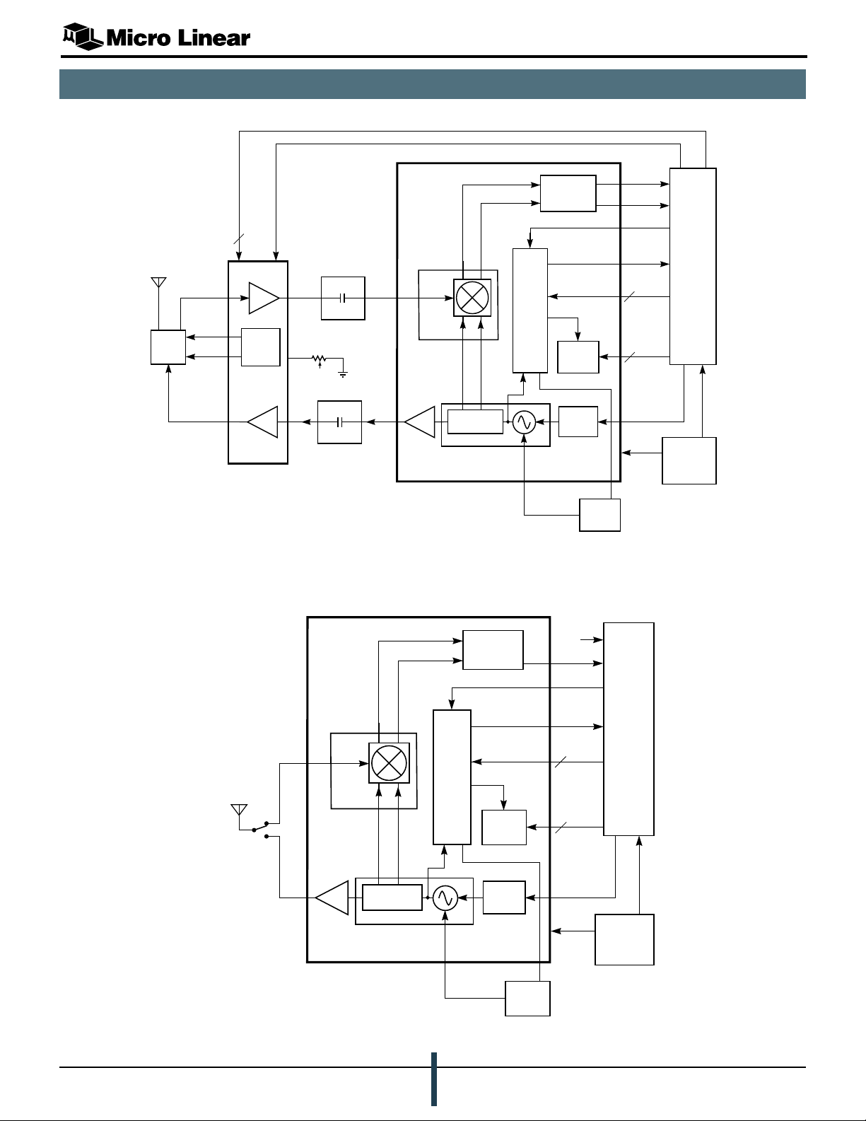
SIMPLIFIED BLOCK DIAGRAMS
ML2721
ANTENNA
RF PIN
DIODE
SWITCH
PINB
PIN
FEEN
2
PAON
ML2751
SWITCH
DRIVERS
TX RF
PA + DRIVER
QPO
LOOP
FILTER
DOUT
RSSI
REF
LD
3
3
DIN
VCCA
CLK,
DATA,
EN
XCEN,
RXON,
PLLEN
BASEBAND
IC
BATTERY
AND
PROTECTION
CIRCUITS
ML2721
TPS
RRFO
RF
TPA
TRFI
LC
FILTER
LC
FILTER
RRFI
TRFO
TX RF
BUFFER
IMAGE
REJECT
MIXER
QUADRATURE
DIVIDE BY 2
1.83GHz VCO
PLL
VTUNE
IF CIRCUITS
CONTROL
LOGIC
TX DATA
FILTER
900MHz DSSS Cordless Phone Application
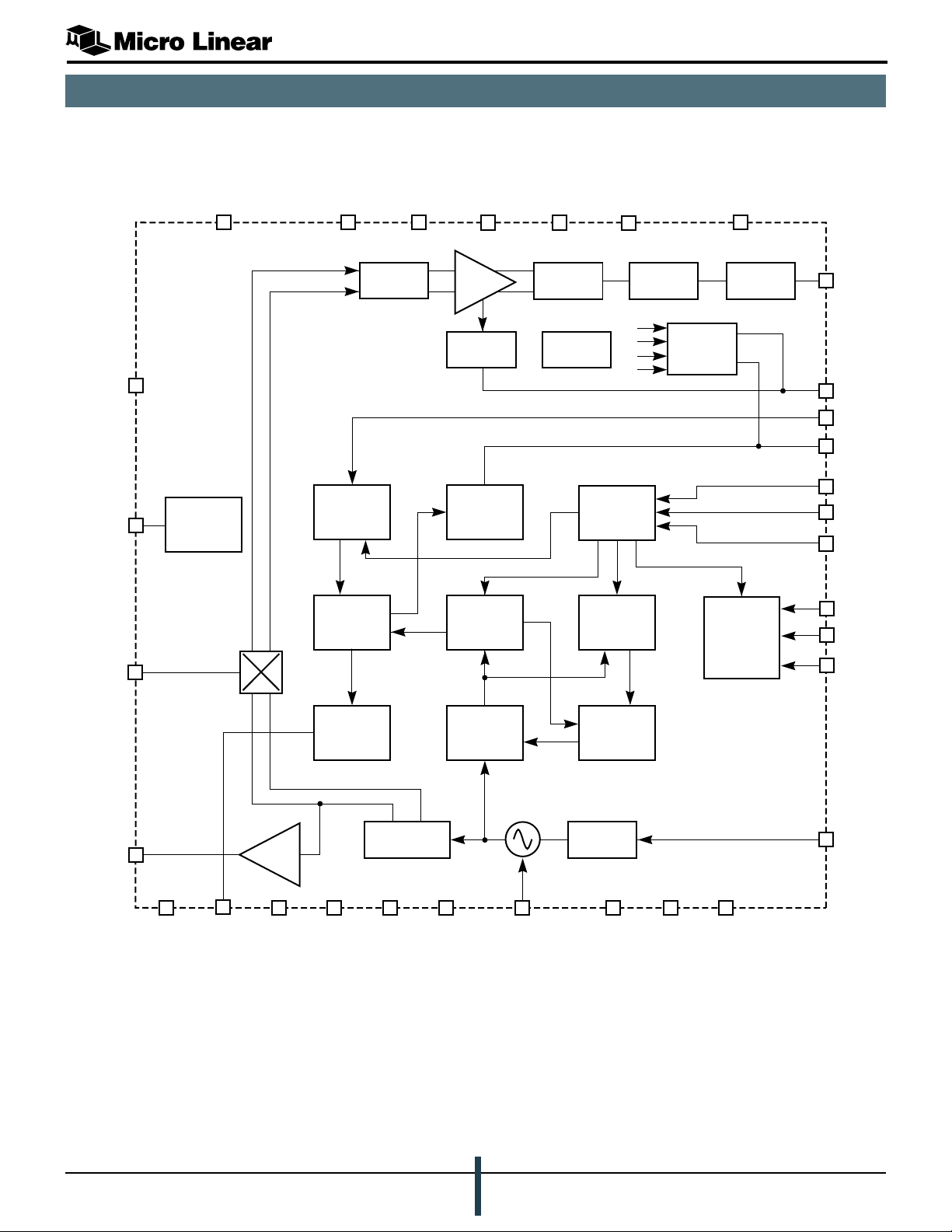
ANTENNA
RRFI
TRFO
ML2721
IMAGE
REJECT
MIXER
TX RF
BUFFER
QUADRATURE
DIVIDE BY 2
1.83GHz VCO
PLL
VTUNE
IF CIRCUITS
CONTROL
LOGIC
TX DATA
FILTER
QPO
LOOP
FILTER
DOUT
RSSI
REF
LD
3
3
DIN
VCCA
CLK,
DATA,
EN
XCEN,
RXON,
PLLEN
BASEBAND
IC
BATTERY
AND
PROTECTION
CIRCUITS
General Purpose FSK Radio
January, 2000
PRELIMINARY DATASHEET
3
Page 4
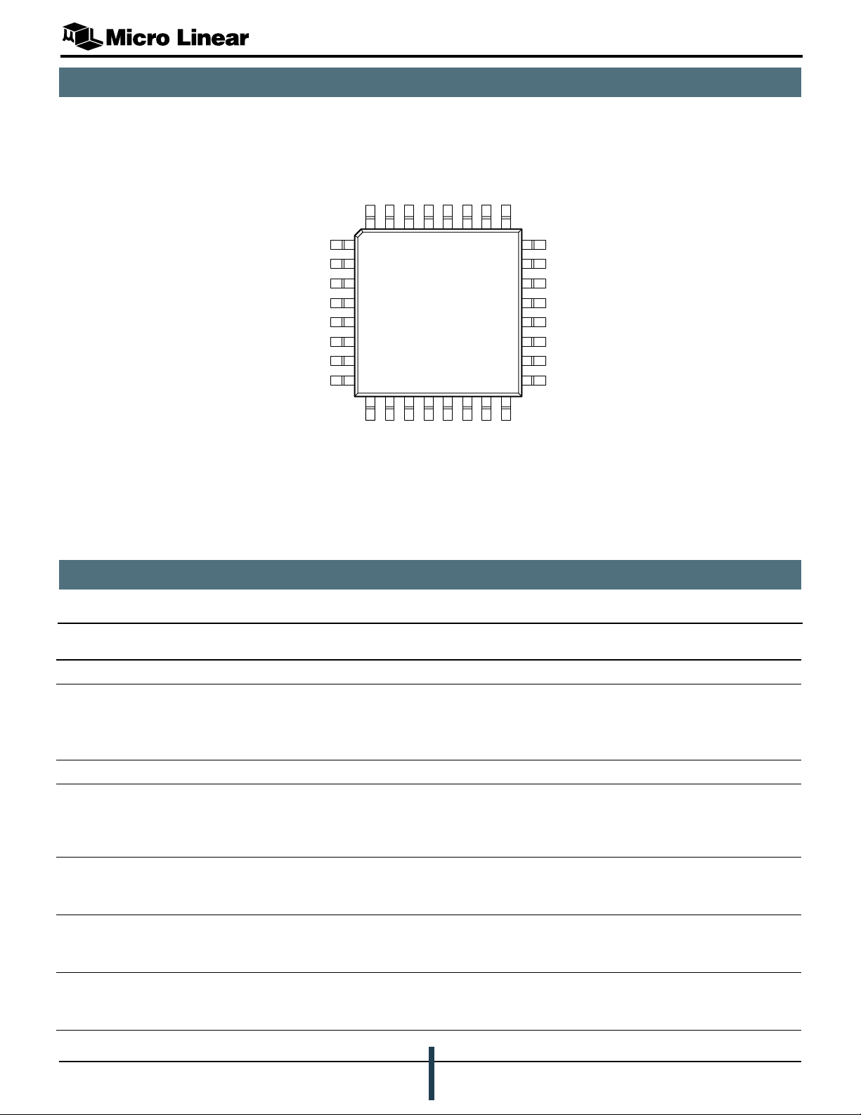
BLOCK DIAGRAM
PRELIMINARY
ML2721
VBG
VCC
RRFI
VDD
31
26
24
5
21
DC
REGULATORS
RX
QUADRATURE
MIXERS
Q
I
RVCC
1
10
REFERENCE
DIVIDER
LO PHASE/
FREQUENCY
DETECTOR
IF
FILTER
RVCC
14
3
RVCC
22
LIMITER
RSSI
LOCK
DETECT
LO 6-BIT
COUNTER
TEST
MUX
VCC
2
13
DATA
SLICER
CONTROL
LOGIC
DOUT
32
RSSI
28
9
REF
7
LD
EN
4
5
DATA
6
CLK
XCEN
1
2
RXON
3
PLLEN
RVCC
4
27
DEMOD
FILTER
ALIGN
6
ADDRESS
DECODE
LO 6-BIT
SWALLOW
COUNTER
RVCC
29
7
DATA
FILTER
TRFO
Q
GND
PRESCALAR
32 / 33
18
1.83GHz VCO
15
VTUNE
PRESCALAR
CONTROL
TX DATA
FILTER
19
GND
20
GND
25
GND
30
DIN
LO CHARGE
PUMP
TX RF
BUFFER
23
8
VSS
11
QPO
LIMITER
12
GND
16
GND
I
QUADRATURE
DIVIDE BY 2
17
GND
4
PRELIMINARY DATASHEET
January, 2000
Page 5
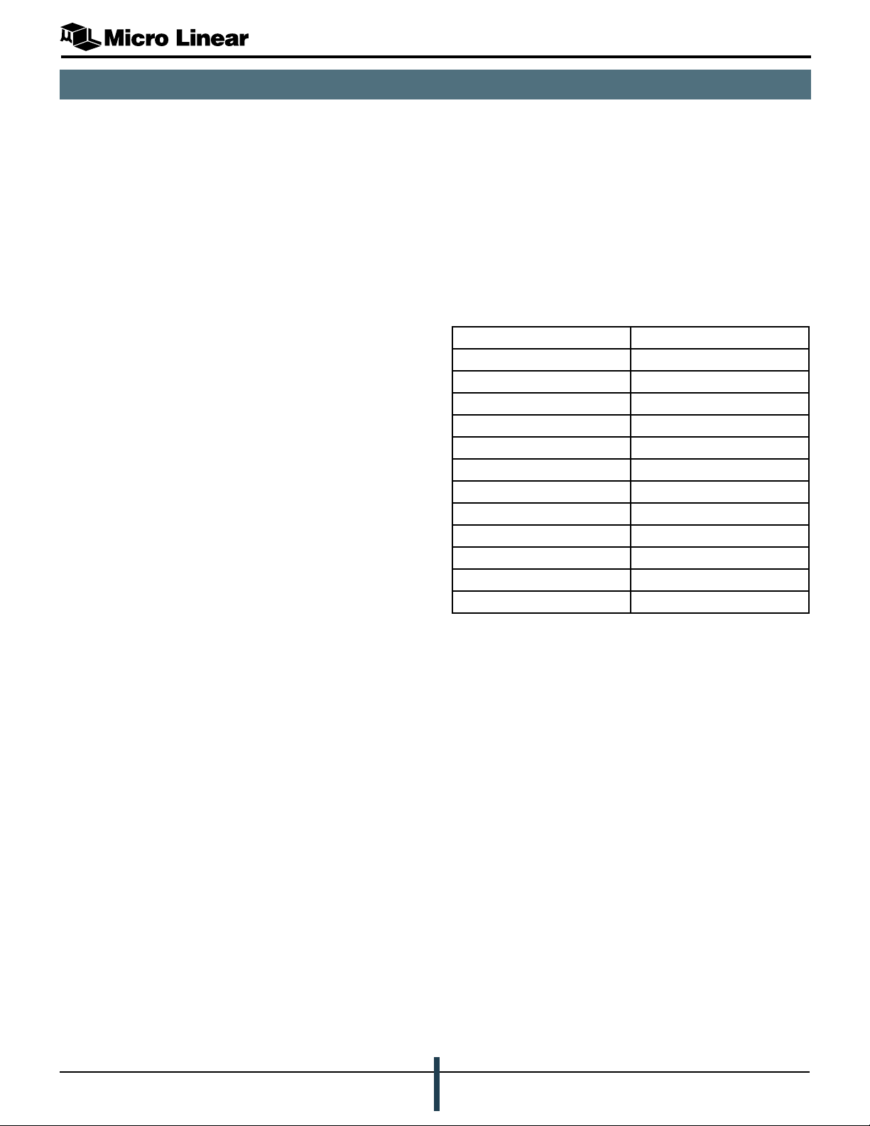
PIN CONFIGURATION
PRELIMINARY
ML2721
32-Pin TQFP (H32-7)
DOUT
VDD
DIN
RVCC7RSSI/TPI
RVCC6VBG
GND
ML2721
XCEN
RXON
PLLEN
EN
DATA
CLK
LD/TPQ
VSS
32 31 30 29 28 27 26 25
1
2
3
4
5
6
7
8
9 10111213141516
REF
1
RVCC
QPO
TOP VIEW
GND
2
VCC
3
RVCC
VTUNE
24
23
22
21
20
19
18
17
GND
VCC
TRFO
RVCC
RRFI
GND
GND
GND
GND
PIN DESCRIPTIONS
Pin # Signal Name I/O Description
5
4
Power & Ground
13 VCC
24 VCC
2
5
16 GND I (analog) DC ground for VCO and LO circuits
10 RVCC
14 RVCC
22 RVCC
27 RVCC
1
3
4
6
I (analog) DC Power Supply Input to the VCO voltage regulator
I (analog) DC power supply Input to Voltage Regulators and unregulated loads:
2.7 to 5.0V. VCC5 is the main (or master) analog VCC pin. There must
be a capacitor to ground from this pin to decouple (bypass) noise and
to stabilize the regulator
O (analog) DC power supply decoupling point for the PLL dividers, phase detector,
and charge pump. This pin is connected to the output of the regulator
and to the PLL supplies. There must be a capacitor to ground from this
pin to decouple (bypass) noise and to stabilize the regulator
O (analog) DC power supply decoupling point for the VCO. Connected to the
output of the VCO regulator. There must be a capacitor to ground from
this pin to decouple (bypass) noise and to stabilize the regulator
O (analog) DC power supply decoupling point for the LO Chain. Connected to the
output of a regulator. There must be a capacitor to ground from this pin
to decouple (bypass) noise and to stabilize the regulator
O (analog) DC power supply decoupling point for Quadrature Mixer and IF filter
circuits. There must be a capacitor to ground from this pin to decouple
(bypass) noise and to stabilize the regulator
January, 2000
PRELIMINARY DATASHEET
5
Page 6

PRELIMINARY
PIN DESCRIPTIONS (continued)
Pin # Signal Name I/O Description
Power & Ground (Continued)
ML2721
29 RVCC
25 GND I (analog) DC Ground to IF, Demodulator, and Data Slicer circuits
12 GND I (analog) Ground for the PLL dividers, phase detector, and charge pump
17 GND I (analog) Signal ground for RF small signal circuits. Pins 17, 18, and 19 should
18 GND I (analog) Ground return for the Receive RF input
19 GND I (analog) Signal ground for the Receive mixers
20 GND I (analog) DC and Signal ground for the Transmit RF Output buffer
31 VDD I (analog) DC power supply input to the interface logic and control registers. This
8 VSS I (digital) Ground for digital I/O circuits and control logic
7
O (analog) DC power supply decoupling point for IF, Demodulator, and Data
Slicer circuits. There must be a capacitor to ground from this pin to
decouple (bypass) noise and to stabilize the regulator
have short, direct connections to each other and additional
connections to ground
supply is not internally connected to any other supply pin, but its
voltage must be less than or equal to the VCC5 supply, and greater
than 2.7V. There must be a capacitor to ground from this pin to
decouple (bypass) noise and to stabilize the regulator
Transmit/Receive
21 RRFI I (analog) Receive RF Input. Nominal impedance at 902 to 928MHz is 50W, with
a simple matching network required for optimum noise figure. This
input is to the base of an NPN transistor and should be AC coupled
23 TRFO O (analog) Transmit RF Output. A broadband 50W output which sources 0dBm
over the 902 to 928MHz range. This output is an emitter follower and
should be AC coupled
Data
30 DIN I (CMOS) Transmit Data input. Drives the transmit pulse shaping circuits. Serial
digital data on this pin becomes FSK modulation on the Transmit RF
output. Data timing is controlled by the logic timing on this pin. The
modulation deviation is determined by internal circuits. This is a
standard CMOS input referenced to VDD &VSS
32 DOUT O (CMOS) Serial digital output after demodulation, chip rate filtering and center
data slicing. A CMOS level output (VSS to VDD) with controlled slew
rates. A low drive output designed to drive a PCB trace and a CMOS
logic input while generating minimal RFI. In digital test modes this pin
becomes a test access port controlled by the serial control bus
Mode Control and Interface Lines
1 XCEN I (CMOS) Enables the bandgap reference and voltage regulators when high.
Consumes only leakage current in standby mode when low. This is a
CMOS input, and the thresholds are referenced to VDD & VSS
2 RXON I (CMOS) Switches the transceiver between Transmit and Receive modes.
Circuits are powered up and signal paths reconfigured according to the
operating mode. This is a CMOS input, and the thresholds are
referenced to VDD & VSS
6
PRELIMINARY DATASHEET
January, 2000
Page 7

PRELIMINARY
PIN DESCRIPTIONS (continued)
Pin # Signal Name I/O Description
Mode Control and Interface Lines (Continued)
3 PLLEN I (CMOS) Enables the PLL at the beginning of a Transmit or Receive slot. Goes
low before data is received or transmitted. RXON and PLLEN define
four distinct operating modes. This is a CMOS input, and the thresholds
are referenced to VDD & VSS
7 LD/TPQ O (CMOS) The Lock Detect output is an open drain output that goes low when the
PLL is in frequency lock. In analog test modes this pin and the RSSI
output become test access points controlled by the serial control bus
9 REF I Input for the 6.144MHz or 12.288MHz reference frequency. This is
used as the reference frequency for the PLL, and as a calibration
frequency for the on chip filters. This is a self-biased CMOS input that
is designed to be driven either by a an AC coupled sine wave source
(recommended coupling capacitor is 470pF) or by a standard CMOS
output
11 QPO O Charge Pump Output of the phase detector. This is connected to the
external PLL loop filter
15 VTUNE I VCO Tuning Voltage input from the PLL loop filter. This pin is very
sensitive to noise coupling and leakage currents
ML2721
26 VBG O Bandgap reference voltage. Decoupled to ground with a 220nF
capacitor
28 RSSI/TPI O Buffered Analog RSSI output with a nominal sensitivity of 33mV/dB.
An RF input signal range of –95 to –15dBm gives an RSSI voltage
output of zero to 2.7V. In analog test modes this pin and the LD output
become test access ports
Serial Bus Signals
4 EN I (CMOS) Enable pin for the three wire serial control bus which sets the
operating frequency and programmable options. The control registers
are loaded on a low to high transition of the signal. Serial control bus
data is ignored when it is high. This is a CMOS input, and the
thresholds are referenced to VDD & VSS
5 DATA I (CMOS) Serial control bus data. 16 bit words which include programming data
and the two bit address of a control register. This is a CMOS input, and
the thresholds are referenced to VDD & VSS
6 CLK I (CMOS) Serial control bus data is clocked in on the rising edge when EN is
low. This is a CMOS input, the thresholds are referenced to VDD & VSS
January, 2000
PRELIMINARY DATASHEET
7
Page 8
PRELIMINARY
FUNCTIONAL DESCRIPTION
ML2721
INTRODUCTION
The ML2721 enables the design and manufacture of low
cost, high performance digital DSSS cordless telephone
transceivers. It can also be used as a general purpose
900MHz transceiver. Integral to the ML2721 is a low IF
receiver whose LO port is driven from an internal
synthesizer. Included are image rejection IF filters,
limiters, discriminator, data slicers, and baseband lowpass
data filters. It also contains internal voltage regulators to
protect critical circuits from power supply noise and
transmit modulation circuits.
The ML2721 has an internal control interface that
programs the synthesizer, the mode of operation, the
external LNA and PA, and provides a convenient and
flexible interface to various baseband processors. For
power level monitoring an RSSI block is included.
The ML2721 is designed to transmit and receive
1.536Mchips signals in 2.048MHz spaced channels in the
902 to 928MHz ISM band. The 1.536Mchips rate with a
15 bit spreading code gives a 102.4kb/s data rate and
provides a 10dB processing gain.
In the Receive mode the ML2721 is a single conversion
low IF receiver. The IF frequency of 1.024MHz results in
an image response in an adjacent channel. An image
reject mixer gives sufficient rejection in this channel. All
IF filtering and demodulation is performed using active
filtering, centered at 1.024MHz. The demodulator is
followed by a matched bit rate filter and a data slicer. The
sliced data is provided to a baseband chip for despreading.
CIRCUIT BLOCK DESCRIPTIONS
PHASE LOCKED LOOP (PLL) AND VOLTAGE
CONTROLLED OSCILLATOR (VCO)
The PLL synthesizes channel frequencies to a 512kHz
resolution, which is more finely spaced than the
1.536MHz signal bandwidth. Non-overlapping channels
are spaced by 2.048MHz where the IF filter and image
reject mixer give a typical adjacent channel rejection of
25dB. There are twelve non-overlapping channels in the
902 to 928MHz ISM band. See Table 1.
lennahCzHMniycneuqerF
1086.309
2827.509
3677.709
4428.909
5278.119
6029.319
7869.519
8610.819
9460.029
01211.229
11061.429
21802.629
Table 1. Non-Overlapping Channel Frequencies
In the Transmit mode the ML2721 uses the Receive mode
VCO and frequency division, with a driver amplifier
providing typically 0dBm output to feed the power
amplifier. The PLL frequency synthesizer loop is opened
during the transmit slot, and the VCO is directly
modulated by low-pass filtered circuits from the internal
modulation filter.
The frequency generation circuits are an internal VCO at
1.83GHz, dividers, a phase comparator and a charge
pump for a PLL frequency synthesizer. The VCO output is
divided by two to produce accurate quadrature outputs at
915MHz. No external components are need for the VCO.
Other modes that are available include power down, and
receive and transmit calibrate, which are discussed in
further detail.
The LO PLL is programmed via a 3-wire serial control bus.
Program words are clocked in on the DATA line (pin 5) by
the CLK (pin 6), and loaded into the dividers or control
circuits when EN (pin 4) is asserted. There is no check for
error in the program words. Once loaded, register contents
are preserved regardless of power conditions. The register
status and operation is independent of the mode of
operation of the PLL.
The reference signal from an external crystal oscillator at
either 6.144MHz or 12.288MHz is fed to a programmable
reference divider. The 1.024MHz reference divider output
is fed to the LO phase frequency detector. The PLL
prescaler input comes from the VCO at 1.83GHz, so the
1.024MHz comparison frequency gives 512kHz frequency
resolution at 902 to 928MHz.
The output of the LO divider is fed to the LO phase/
frequency detector and subsequently to the charge pump.
The dividers and charge pump are disabled during the
active slot to save power.
8
PRELIMINARY DATASHEET
January, 2000
Page 9

PRELIMINARY
CIRCUIT BLOCK DESCRIPTIONS
ML2721
LO VCO AND TRANSMIT DRIVER
The internal LO VCO operates at 1.8 to 1.86GHz, which
is two times the LO frequency of 900 to 930MHz. The
VCO output is divided by 2 to give accurately matched
quadrature signals at 915MHz. In Receive mode the LO is
offset from the wanted signal by +1.024MHz to produce
the low IF. This 1.024MHz shift is produced by
automatically adding an offset of +2 counts to the PLL
divider programming.
In Transmit mode the LO is frequency modulated by the
transmitted data, using a modulation port of the VCO. The
VCO output is divided by 2 and a driver amplifier
typically develops 0dBm at 900 to 930MHz to directly
drive an ML2751 power amplifier.
TRANSMIT DATA FILTER AND MODULATION DRIVER
Logic level NRZ signals at DIN are scaled and filtered by
th
a 5
-order lowpass filter. The lowpass filter is tuned to
give a 1.35MHz 3dB point to pass the 1.536Mchips
transmit data. The filter data is then fed to the internal
modulation port of the LO tank circuit.
In the transmit closed loop mode the modulation port is
held at its midpoint so that the synthesizer locks to the
center channel frequency. In the transmit open loop mode
the VCO is modulated by Gaussian filtered data via the
VCO modulation port. The modulation driver contains
scaling circuitry to control the FM deviation over the
entire VCO tuning range. This circuit is inactive in the
receive mode.
DATA FILTER AND DATA SLICER
The FM demodulator is followed by a Gaussian lowpass
filter whose 768kHz cutoff frequency is matched to the
transmitted 1.536Mchip/s waveform. This Gaussian filter is
implemented with similar circuits to the IF filter, and is
shared with the Transmit modulation path. The filter output
can be AC coupled to the slicer because the spreading
code is almost DC balanced. The data slicer signal is
output to the baseband processor for timing recovery and
decoding.
POWER SUPPLY
The ML2721 uses multiple voltage regulators to protect
sensitive internal circuits from power supply noise.
Separate regulators supply the PLL dividers, RF circuits
and IF circuits. Each of these regulators takes its power
from VCC5, and supplies power internally to its respective
RVCCn pin. External capacitors are required at each
RVCCn pin to decouple the outputs of the internal
regulators. The VCO regulator takes its power from the
VCC2 pin which is normally connected to the RVCC6 pin.
An external decoupling capacitor is also used on the
internal bandgap voltage reference to improve the noise
performance of the regulators.
These regulators are effective at supply voltages from
3.0V to 5.0V. As the VCC5 supply voltage drops below
3.0V chip performance gradually degrades, but the
ML2721 transceiver will maintain the link as long as the
supply voltage is greater than 2.7V.
RECEIVE MIXERS AND IF CHAIN
The Receive RF quadrature mixers down-convert the
signal to the 1.024MHz receiver IF. The input of the mixer
is single-ended and matched to 50W by a series inductor.
This gives a good terminating impedance for the
preceding RF filter. The quadrature outputs of the down
converter feed the IF filter. The quadrature mixer and IF
filter together achieve a typical image rejection of 35dB.
A quadrature combiner for the image reject mixer and a
12th-order Gaussian bandpass filter make up the active IF
filters. The active filters provide an accurate Gaussian
characteristic with a 1.408MHz, 3dB bandwidth which
improves both sensitivity and adjacent channel rejection.
The IF amplifiers provide the bulk of the receiver’s gain.
An RSSI signal is generated by using the outputs of the IF
amplifiers. The RSSI signal is conditioned and sent to the
baseband controller. A frequency-to-voltage converter
provides highly linear FM demodulation with good data
recovery from the low IF.
January, 2000
PRELIMINARY DATASHEET
9
Page 10

MODES OF OPERATION
PRELIMINARY
ML2721
OVERVIEW
n STANDBY: All circuits powered down, except the
control interface (Static CMOS)
n RXCAL: Receive Calibration. PLL lock up time and
IF filter alignment, prior to RECEIVE
n RECEIVE: Receiver circuits active
n TXCAL: Transmit Calibration. PLL lock up time prior
to TRANSMIT
n TRANSMIT: PLL open loop, modulated RF output
available from IC
The four operational modes are RXCAL, RECEIVE, TXCAL
and TRANSMIT. They are set by the RXON (pin 2) and
PLLEN (pin 3) control pins. XCEN (pin 1) is the chip
enable/disable pin and can be set for standby operation.
The relationship between the parallel control lines and the
mode of operation of the IC is given in Table 2.
PARALLEL MODE CONTROL
NECXNOXRNELLPedoM
0XX YBDNATS
111 LACXR
110 EVIECER
10 1 LACXT
100 TIMSNART
Table 2. Mode Selection
The ML2721 is intended for use in TDD and TDMA radios
in battery powered equipment. To minimize power
consumption it is designed to switch rapidly from a low
power mode (STANDBY) to receive or transmit. The
ML2721 can also make a quick transition from receive to
transmit for TDD operation. Prior to transmitting or
receiving time should be allowed for the PLL to lock up,
and in the case of receive, for the IF filters to be aligned.
The ML2721 operates as a TDD radio on one RF frequency
(transmit or receive). The VCO frequency changes
between receive and transmit functions because of the IF
frequency. This VCO frequency step is automatically
performed.
ILO
RECEIVE MODES
RXCAL AND RECEIVE
In RECEIVE mode, the received signal at 900MHz is down
converted, bandpass filtered (IF filter), fed to the
frequency-to-voltage converter and low-pass filtered. The
output of the low-pass filter is fed to the data slicer which
outputs NRZ digital data. An RSSI voltage output
indicates the signal level at the output of the IF filter.
Prior to receive mode the ML2721 should be switched to
RXCAL mode. This is to allow the IF filters to be aligned
and for the PLL to switch frequency and settle to the
required frequency for receiving. Filter alignment, using
the Reference Frequency input signal REF, in the RXCAL
mode sets:
n Discriminator center frequency
n IF filter center frequency and bandwidth
n Receiver data low pass filter bandwidth
n Transmit data low pass filter bandwidth
In receive mode the programmed center frequency sets
the RF channel that will be received. This means the PLL
center frequency is the programmed RF center frequency
plus the IF frequency. The frequency offset required for the
low frequency IF in the RXCAL mode is automatically
calculated and performed.
RECEIVER CIRCUIT OPERATION
The ML2721 receive chain is a low IF receiver using
advanced integrated radio techniques to eliminate
external IF filters and minimize external RF filter
requirements. No external support circuitry is required
other than supply decoupling and input matching. The
precise filtering and demodulation circuits give improved
performance over conventional radio designs using
external filters. See Figure 1.
10
RECEIVER
INPUT
RX
I.F. FILTER
QLO
Figure 1. Receiver Block Diagram
PRELIMINARY DATASHEET
LIMITING
AMPLIFIERS
F V
RSSI
AGC
January, 2000
DATA FILTER
DOUT
∫
RSSI
Page 11

PRELIMINARY
MODES OF OPERATION (CONTINUED)
ILO
ML2721
DATA FILTER
QLO
FREF or
FREF/2
Figure 2. Dual Modulus Signal Divider
The signal flow in RECEIVE mode is from the RF input,
through an image reject mixer, IF filter, hard limiter,
Frequency to Voltage converter, data filter and data slicer.
The ML2721 uses a single conversion super heterodyne
receiver with a nominal IF of 1.024 MHz. An AGC
subsystem extends the dynamic range of the receiver. The
IF frequency and filter bandwidths are given in Table 3.
oitaRnoisiviDecnerefeR621
retemaraP0=0DR1=0DR
ycneuqerfretnecretlifFI6/FER21/FER
htdiwdnabretlifFI4.4/FER8.8/FER
retlifatadevieceR8/FER61/FER
ycneuqerfretnecretrevnocVotF6/FER21/FER
Table 3. Filter Parameters to Division Ratio
Major features of the receiver are:
n High dynamic range mixers with 10dB noise figure, –
15dBm IP3, 35dB image rejection (typical)
n 6-pole bandpass IF filter, with accurate Gaussian to
12dB response
n Center frequency 1.024MHz, Bandwidth 1.408 MHz
(nominal)
CAL
TONE
GEN
F V
FCOMP
I
Q
TRACKING
COUNTER
∫
FILTER ALIGNMENT
In RXCAL mode the receiver is not functional. Instead, the
ML2721 filter alignment function tunes all the internal
filters using the reference frequency from the REF pin. See
Figure 2.
The IF filter, data filters, and the F-to-V converter all have
their frequency responses governed by RC time constants.
Every capacitor that affects the frequency response
includes a binary weighted capacitor array controlled by
a 7 bit tuning bus. In RXCAL mode a reference tone at the
IF center frequency is routed to the F-to-V converter. A
digital tracking loop then adjusts the tuning word until
there is mid-rail output from the F-to-V converter. This
tracking loop may take up to 300µs to tune the filter when
XCEN is asserted, but the tracking loop will continue to
make small adjustments whenever the ML2721 is in
RXCAL mode. Because all the filters in the chip are tuned
in this manner, centering the F-to-V converter sets up the
correct center frequencies and bandwidths for all the
filters.
The ML2721 must be placed in RXCAL mode for 300µs
whenever XCEN is asserted to give time for the filters to
align completely.
Data Slicer
n Limiting IF amplifiers with >80dB gain, and excellent
AM rejection
n AGC to extend the dynamic range of the integrated
filters & RSSI
n Logarithmic RSSI output from Limiter; AGC state is
information added to give 80dB range
n FM demodulation by a linear F-to-V converter
n 5-pole low-pass data filter with an accurate Gaussian
response and 3dB cutoff at 768kHz (nominal)
n 2 level data slicer with DC offset removal
The output of the receiver is quantized in amplitude (to 1
bit) but there is no internal timing recovery. Timing
recovery is performed in the external baseband circuits.
January, 2000
The data slicer is a comparator that is AC coupled to the
receive data filter output. The output is logic high or logic
low. This circuit is designed to rapidly acquire valid data
at the beginning of a received packet of data. The
nominal time constant for the AC coupling is 9µs. This
limits the maximum recommended run length to four ones
or zeroes at 1.3Mbps. Longer run lengths require the use
of a more complex external data slicer circuit.
Data Output Drive
The ML2721 D
pin is designed to drive a PCB trace
OUT
and a single logic input with controlled slew rates. Buffer
the output when driving any logic load greater than 5pF
(
i.e.
, more than an ´10 oscilloscope probe or a single
CMOS logic input pin).
PRELIMINARY DATASHEET
11
Page 12

OVERVIEW (continued)
PRELIMINARY
ML2721
TRANSMIT MODE
TXCAL AND TRANSMIT
In TRANSMIT mode, the VCO is directly modulated with
filtered FSK transmit data. The PLL is disabled or open,
with the charge pump output tri-stated. This stops the PLL
from contending with the applied modulation. The digital
transmit data input is generated by external baseband
circuits. This input signal is level shifted and filtered by the
transmit modulation filter prior to modulating the VCO
frequency. Due to the low leakage current of the charge
pump and tank circuit the ML2721 can be in TRANSMIT
mode for slot lengths of up to 10ms.
During RXCAL mode the transmit modulation data filter is
automatically tuned to remove the need for production
alignment. When the ML2721 is powered up (VDD first
applied) the tuning information is reset to mid-range. The
filter alignment mode should be used after power up or
XCEN enabled, and prior to transmission. This ensures the
modulation filters are aligned to prevent unwanted
spurious emissions.
Prior to transmitting the PLL must tune to the intended RF
center frequency of the transmission. This occurs in TXCAL
mode. The Transmit modulation is disabled and any input
on the DIN pin is ignored. The transmit output buffer is
enabled during TXCAL mode. To prevent spurious emissions
due to the PLL locking, any external RXON switch or PA
should be disabled during TXCAL mode.
Transmitter Circuit Operation
The ML2721 transmitter is a 2-FSK transmitter using a
directly modulated open loop VCO. See Figure 3. This
type of transmitter is simple, low power, and well suited
to a time-slotted system. The transmitter uses the stored
VCO tuning voltage on the PLL loop filter to set the VCO
frequency for the duration of the transmit slot. The
modulation is introduced through a second VCO tuning
port. This modulation port has a much lower tuning
sensitivity than the main tuning port in order to produce
the ±550kHz FSK deviation. Compensation circuits
stabilize the modulation deviation over the VCO tuning
range, and internal logic manages the correct transition
from TXCAL to TRANSMIT mode. The ML2721 design
supports transmit slot lengths up to 10ms, and the time
required to set up the transmitter for a new slot (TXCAL
mode) is 70µs.
The operating cycle of the transmitter starts with TXCAL
mode. See Figure 4. The data filter input is zeroed and the
PLL locks the VCO frequency to the desired RF channel
center frequency. A CW signal at the selected RF channel
frequency comes out of the Transmit RF output. When the
PLLEN control line is de-asserted the transmitter starts its
transition to TRANSMIT mode. The PLL charge pump is
disabled, leaving the PLL loop filter to hold the correct
tuning voltage for this channel. The data formatter injects
an NRZ bipolar data waveform into the Transmit data
filter. The Transmit data filter band-limits this waveform,
and feeds it to the modulation compensation circuits.
These scale the modulation voltage (depending on the
VCO tuning voltage) and drive the VCO tuning port with
TUNING
PORT
TRANSMIT
RF OUTPUT
12
TRANSMIT
DATA FILTER
MODULATION
COMPENSATION
LOOP FILTER
MODULATION
PORT
VCO
DIVIDE
BY 2
Figure 3. Transmitter Block Diagram
DIVIDER
12
N
PRELIMINARY DATASHEET
P D
DIN
VHIGH
VLOW
VMID
PLLEN
RXON
PLLEN
DATA FILTER
INPUT
DATA FILTER
OUTPUT
VCO TUNING
PORT VOLTAGE
OUTPUT
FREQUENCY
ON TRFO PIN
Figure 4. Transmitter Operating Cycle
January, 2000
Page 13

OVERVIEW (continued)
PRELIMINARY
ML2721
the scaled, filtered modulation. The voltage on the
modulation port swings above and below its central value
to produce 2-FSK modulation on the VCO. The modulation
filtering is sufficient to meet the FCC occupied bandwidth
and out-of-band emissions requirements, and does not
introduce significant ISI (Inter Symbol Interference).
The Transmit modulation filter is a 5
th
order all-pole filter,
designed for minimum differential group delay and good
stop band attenuation at greater than 2MHz. The 3dB
retemaraP
lanimonretlifatadtimsnarT
htdiwdnabBd3
6ybediviD
)0=0DR(
4.4/FER8.8/FER
Table 4. Bandwidth as a Function of Divider Ratio
21ybediviD
)1=0DR(
bandwidth of the filter is slaved to the reference
frequency. See Table 4.
FCOMPNX FCOMP
PLEN
P D
LOOP FILTER
VCO
DIVIDER
may be disturbed, and the radio could transmit on an outof-band signal. To prevent this a comparator monitors the
supply voltage and trips a transmitter shutdown latch if
the supply voltage drops below 2.6V. This disables the
transmitter output buffer. The latch is reset by the next
rising edge of RXON so that the radio cannot transmit
RXON
PLLEN
VCCA
SUPPLY
VOLTAGE
TRANSMIT
LOCKOUT
TRANSMIT
R.F. OUTPUT
2.65V
LATCH
Figure 6. Transmitter Low Voltage Lockout Sequence
until the next complete transmitter cycle. See Figure 6. If
the ML2721 is DC powered on with RXON enabled the
transmitter buffer will be latched off. This helps prevent
unwanted emissions.
12
DIVIDE
BY 2
NX FCOMP/2
INPUT SIGNAL AT
N X FCOMP/2
ADDER
2N
REGISTER 1
BIT14...BIT3
IF AT FCOMP
Figure 5. Transmitter Eye Diagram
Figure 5 shows an eye diagram recovered from the
Transmit RF output of the transceiver with a data stream of
1.5Mb/s.
Transmitter Lockout (Low Voltage)
The ML2721 transmitter features a low voltage lockout
circuit to meet FCC spurious emissions requirements. If
the supply voltage drops below 2.5V the VCO frequency
F/6
F/12
FREF
FCOMP
Programming the ML2721 integrated PLL.
For ease of use, the ML2721 PLL is programmed to the set
RF center frequency of operation of the radio. See Figure
7. The RF output center frequency is half the VCO
frequency during transmission. The VCO is automatically
offset by twice the IF, to give the correct receive LO
frequency, during reception. This guarantees the baseband
PLLEN
FCOMPN × FCOMP
N
NX FCOMP/2
VCO
TRANSMIT
RF BUFFER
DIVIDE
BY 2
LOOP FILTER
DIVIDER
12
ADDER
O
REGISTER 1
BIT14...BIT3
P D
FCOMP
÷6 or
÷12
REF
January, 2000
Figure 7. Phase Locked Loop in Transmit Mode
PRELIMINARY DATASHEET
13
Page 14

PRELIMINARY
MODE OF OPERATION (CONTINUED)
ML2721
circuits do not reprogram the PLL for every receive or
transmit packet. The PLL divide register should be
programmed with a binary integer which represents the
desired RF channel frequency divided by 0.512 MHz
(when using a 6.144 or 12.288MHz reference frequency).
When in TRANSMIT mode the PLL is disabled and the
loop opened to allow modulation of the VCO. The VCO
runs at twice the channel frequency, and the Transmit RF
output is taken from one output of the quadrature divider.
The PLL locks during TXCAL mode.
The frequency plan for the PLL and VCO transmit is given
in Table 5.
When in RECEIVE mode the PLL is disabled to conserve
power and prevent PLL divider noise from desensitizing
the receiver. See Figure 8. The PLL frequency is set to
give a LO frequency equal to the desired RF channel
frequency plus the IF frequency. The VCO signal is
divided by two to provide the quadrature LO for the
image reject down convert mixer. The PLL locks during
RXCAL mode.
retemaraPalumroFeulaVsnoitinifeD
retsigerycneuqerflennahcFRN
ycneuqerftuptuoFRtimsnarTN
´
)2/PMOCF(zHM039ot009morfegnarehtrevocotdeetnarauG
oitarnoisividLLPN
ycneuqerfOCVN
´
PMOCFzHG68.1ot08.1siegnaR
ycneuqerfnosirapmocLLP)zHM1~(PMOCF
noituloserycneuqerF2/PMOCFtuptuoFRtimsnarTtA
INPUT SIGNAL AT
N × FCOMP/2
4201
£N£
2671
£N£
rotarapmoc
LOOP FILTER
VCO
(N+2) × FCOMP
÷2
N × FCOMP/2
Figure 8. Phase Locked Loop in Receive Mode
DIVIDER
12
ADDER
2
REGISTER 1
BIT14...BIT3
IF AT FCOMP
PLLEN
FCOMP
÷6 or
N
.egnarredividetelpmocehtrof3904
.dnabMSIzHM829ot209ehtrof2181
esahpehtdnaOCVehtneewtebnoisividycneuqerfehT
.21ro6ybdedividycneuqerftupniFER
P D
FCOMP
÷12
REF
.)OPQ(tuptuopmupegrahctasesluppmupegrahcfoetaR
14
Table 5. Transmit Mode Frequency Relationsships
retemaraPalumroF/eulaVsnoitinifeD
retsigerycneuqerflennahcFRN
ycneuqerflennahCN
ycneuqerfOL
´
)2/PMOCF(zHM039ot009morfegnarehtrevocotdeetnarauG
)2+N(
´
)2/PMOCF(
ycneuqerfFIzHM0.1~ycneuqerflennahcdnaycneuqerfOLneewtebecnereffiD
oitarnoisividLLP2+N
ycneuqerfOCV)2+N(
´
PMOCFzHG68.1ot08.1siegnaR
ycneuqerfnosirapmocLLP)zHM0.1~(PMOCF
noituloserycneuqerF2/PMOCFtuptuoFRtimsnarTtA
Table 6. Receive Mode Frequency Relationships
PRELIMINARY DATASHEET
4201
£N£
2671
£N£
rotarapmoc
January, 2000
egnarredividetelpmocehtrof3904
dnabMSIzHM829ot209ehtrof2181
reximreviecerehtfostropOLehttA
esahpehtdnaOCVehtneewtebnoisividycneuqerfehT
)OPQ(tuptuopmupegrahctasesluppmupegrahcfoetaR
21ro6ybdedividycneuqerftupniFERF
Page 15

PRELIMINARY
MODE OF OPERATION (CONTINUED)
ML2721
The ~1MHz frequency shift is achieved by internally
adding an offset of +2 counts to the PLL divider register
value. The relationship between the LO frequency, the
programmed RF channel frequency, and the reference
frequency in RECEIVE mode is given in Table 6.
VCO OPEN AND CLOSED LOOP OPERATION
Normally the PLL is only operational in RXCAL and
TXCAL modes, when a closed loop PLL is formed. The PLL
is a conventional single loop integer division PLL. The
phase comparator has a charge pump output so that an
external passive loop filter can be used. The PLL dividers
support integer main divider ratios between 1024 and
4095, and reference divider ratios of 6 and 12.
In RECEIVE and TRANSMIT modes the PLL loop is opened
and the stored VCO tuning voltage (on the loop filter)
maintains the VCO at the desired frequency. In open loop
modes the PLL charge pump is shut off and the PLL
circuits are shut down to save power. Interlock logic
manages the start up and shut down of the PLL to ensure
that the VCO frequency is not disturbed in the transition
between modes. If better frequency stability is required
the RXCL bit in the PLL configuration register allows the
PLL to remain in the closed loop mode during RECEIVE
mode. The PLL loop must be opened in TRANSMIT mode,
as the PLL would otherwise attempt to remove the FM
transmit modulation.
dielectric absorption and low leakage current. Ceramic
capacitors can be used, but care should be taken with
applications where there is significant thermal or
mechanical shock.
STANDBY MODE
In STANDBY the ML2721 transceiver is powered down.
The only active circuits are the control interfaces, which
are static CMOS to minimize power consumption. The
serial control interface (& control registers) remain
powered up and will accept and retain programming data
as long as the digital supply is present. The ML2721 serial
control registers should be loaded with control and
configuration data before any active mode is selected.
The filter alignment registers are reset at power up.
TEST MODE
Special test access circuitry is needed for IC production
test and radio debugging because of the RF to digital
functionality of the ML2721. Two analogue test outputs
(RXTPI and RXTPQ) are multiplexed with the RSSI and
lock detect (LD) output pins, and digital test outputs are
multiplexed onto the received data output pin (DOUT).
The test multiplexers are controlled by a test register
accessed over the serial control bus.
PLL LOOP FILTER DESIGN
The PLL loop filter performs a dual function. In the closed
loop modes (RXCAL and TXCAL) it acts as a second order
loop filter, and in the open loop modes (TRANSMIT,
RECEIVE without RXCL) it holds the VCO tuning voltage
for the duration of the data slot. The correct loop filter
component values are a function of the desired closed
loop bandwidth, loop response damping factor charge
pump current, VCO tuning sensitivity and PLL division
ratio. The charge pump current, VCO tuning sensitivity,
and division ratio range are fixed by the on chip circuits,
so the only independent variables are the PLL’s closed
loop bandwidth and damping factor.
The recommended values of 47nF, 360W and 3.3nF give a
50kHz closed loop bandwidth and a damping factor of 0.8
for robust closed loop operation. (18nF, 430W and 1.8nF
reduce the damping factor to 0.72; 33nF, 390W and 470pF
set the damping factor at 0.9). Plastic film capacitors are
used on the application circuit because of their excellent
January, 2000
PRELIMINARY DATASHEET
15
Page 16

CONTROL INTERFACES
PRELIMINARY
ML2721
There are two control interfaces:
Parallel mode control. Controlling the mode of
operation of the ML2721. Refer to the Operational
Modes section for details.
Serial Interface. Programing the PLL signal and
reference dividers, internal test modes, and filter
alignment.
Other signal interfaces to the IC are:
n Receiver data output
n Transmit modulation data input
n PLL lock detect output, to indicate when the on chip
PLL is in frequency lock
n Receive RF input, the input to the receiver circuits
n Transmit RF output, the output for the modulated RF
signal
n Received signal strength output: RSSI indicates the
power of the received signal
n Reference frequency input for PLL dividers
Bit Allocations
Data words are entered beginning with the MSB. The word
is divided into a leading 14-bit data field and a 2-bit
address field. When the address field has been decoded
the destination register is loaded on the rising edge of EN.
Providing less than 16 bits of data will result in
unpredictable behavior when EN goes high.
Parallel Interface
The chip is enabled by the XCEN (Transceiver enable)
signal. The operating mode is set by the two control lines
TX/RX (Transmit/Receive Mode) and PLLEN (PLL enable),
and the 3 wire serial data bus. The logic for XCEN, RXON
and PLLEN is given in Table 7.
NECXNOXRNELLPemaNedoMedoMpihC
0XX ffOffO
10 1 LACXTpooldesolcrezisehtnystimsnarT
10 0 XTdetaludomdnapoolneporezisehtnystimsnarT
111 LACXRngilaretlifdnapooldesolcrezisehtnysevieceR
110 XRnoevieceR
Table 7. Control Logic
16
PRELIMINARY DATASHEET
January, 2000
Page 17

PRELIMINARY
CONTROL INTERFACES AND REGISTER DESCRIPTION (continued)
ML2721
REGISTER INFORMATION
A unidirectional three wire serial bus is used to set the
ML2721’s transceiver parameters and to program the PLL
circuits. Programming is performed by entering 16-bit
words into the ML2721 serial interface. Four 16-bit
registers are partitioned such that 14 bits are dedicated for
data to program the operation and 2 bits are used for
register addressing. Only three of the registers should be
used in normal operation. The purpose of each of the
registers is:
n Register 0: PLL configuration;
n Register 1: PLL tuning data;
n Register 2: Internal test access;
n Register 3: Reserved for production test only.
Register 0: PLL Configuration Register
14-bit Register Data
DB8
DB7B9DB6B8DB5B7DB4B6DB3B5DB2B4DB1B3DB0B2ADR1B1ADR0
B10
DB13
MSB
Res.
DB12
B15
DB11
Res. Res. Res. Res. Res. Res. Res. Res. Res. LOL RCXL RD0 QPP 0 0
B14
B13
DB10
B12
DB9
B11
Table 8 shows a register map. Table 9 provides a detailed
diagram of the register organization: Table 9a and 9b
outline the PLL configuration and channel frequency
registers, and Table 9c displays the filter tuning and test
mode register.
2-bit Register Address
B0
Register 1: RF Channel Frequency Register
MSB
DB13
Register 2: Filter Tuning Select and Text Mode Access Register
DB13
Register 3: Production Register (not for customer use)
DB13
Res.
B15
MSB
TMODE
B15
MSB
Res.
B15
DB12
DB12
DB12
DB11
Res. CHQ11 CHQ10 CHQ9 CHQ8 CHQ7 CHQ6 CHQ5 CHQ4 CHQ3 CHQ2 CHQ1 CHQ0 0 1
B14
DB11
Res. Res. Res. Res. Res. Res. Res. DTM2 DTM1 DTM0 ATM2 ATM1 ATM0 1 0
B14
DB11
Res. Res. Res. Res. Res. Res. Res. Res. Res. Res. Res. Res. Res. 1 1
B14
B13
B13
B13
DB10
DB10
DB10
B12
B12
B12
DB9
B11
DB9
B11
DB9
B11
14-bit Register Data
DB8
14-bit Register Data
DB8
14-bit Register Data
DB8
16-bit Register Data
2-bit Register Address
DB7B9DB6B8DB5B7DB4B6DB3B5DB2B4DB1B3DB0B2ADR1B1ADR0
B10
16-bit Register Data
2-bit Register Address
DB7B9DB6B8DB5B7DB4B6DB3B5DB2B4DB1B3DB0B2ADR1B1ADR0
B10
16-bit Register Data
2-bit Register Address
DB7B9DB6B8DB5B7DB4B6DB3B5DB2B4DB1B3DB0B2ADR1B1ADR0
B10
B0
B0
B0
Note: DB=Data Bit, ADR=Address Bit, Res.=Reserved.
16-bit Register Data
Table 8. Register Organization
January, 2000
PRELIMINARY DATASHEET
17
Page 18

PRELIMINARY
CONTROL INTERFACES AND REGISTER DESCRIPTION (continued)
tiBataDemaNnoitpircseDesU
31BD/)BSM(51BdevreseR
21BD/41BdevreseR
11BD/31BdevreseR
01BD/21BdevreseR
9BD/11BdevreseR
8BD/01BdevreseR
7BD/9BdevreseR
6BD/8BdevreseR
5BD/7BdevreseR
4BD/6BdevreseR
3BD/5BLOLtfihSycneuqerFLLP
2BD/4BLCXR
1BD/3B0DRtceleSycneuqerFecnerefeR
0BD/2BPPQytiraloPpmuPegrahCLLP
1BDA/1B1RDA0=1RDA
0BDA/)BSL(0B0RDA0=0RDA
noitarepO
evieceRlamroNniedoMLLP
.evieceRgnirudpoolnepoLLP:0
ML2721
)orez(0otstiBllAteS
.evieceRrofzHM420.1,timsnarTrofzH0sitfihsOL:0
.evieceRrofzH0,timsnarTrofzHM420.1sitfihsOL:1
.evieceRgnirudpooldesolcLLP:1
.ycneuqerfecnereferlanimonzHM441.6:0
.ycneuqerfecnereferlanimonzHM882.21:1
.tnerrucsknispmupegrahC;.fer.qerf>.gis.qerF:0
.tnerrucsecruospmupegrahC;.fer.qerf<.gis.qerF:1
Table 9A. Register 0 — PLL Configuration Register
tiBataDemaNnoitpircseDesU
31BD/)BSM(51BdevreseR
21BD/41BdevreseR
11BD/31B11QHC
01BD/21B01QHC
9BD/11B9QHC
8BD/01B8QHC
7BD/9B7QHC
6BD/8B6QHC
5BD/7B5QHC
4BD/6B4QHC
3BD/5B3QHC
2BD/4B2QHC
1BD/3B1QHC
0BD/2B0QHC
1RDA/1B1RDAtibsserddaBSM0=1RDA
0RDA/)BSL(0B0RDAtibsserddaBSL1=0RDA
tfihsycneuqerfLLP
stibtcelesycneuqerflennahC
tfihsycneuqerfecnerefeR
)orez(0otstibllateS
f=oitarediviD
215.0/
C
sknispmupegrahC;.fer.qerf>.gis.qerF:0
18
Table 9B. Register 1 — Channel Frequency Register
PRELIMINARY DATASHEET
January, 2000
Page 19

PRELIMINARY
CONTROL INTERFACES AND REGISTER DESCRIPTION (continued)
tiBataDemaNnoitpircseDesU
31BD/)BSM(51BEDOMTtiBtceleSretlifenuTnoitarepOlamroNrof0otEDOMTteS
21BD/41BdevreseR
11BD/31BdevreseR
01BD/21BdevreseR
9BD/11BdevreseR
8BD/01BdevreseR
7BD/9BdevreseR
6BD/8BdevreseR
5BD/7B2MTD
stiBlortnoCtseTlatigiD31elbaTeeS4BD/6B1MTD
3BD/5B0MTD
2BD/4B2MTA
stiBlortnoCtseTgolanA21elbaTeeS1BD/3B1MTA
0BD/2B0MTA
1BDA/1B1RDAtiBseerddABSM1=1RDA
0BDA/)BSL(0B0RDAtiBseerddABSL0=0RDA
ML2721
)orez(0otstiBllAteS
Table 9C. Register 2 — Filter Tuning Select and Test Mode Register
Serial Interface
Data and clock signals are ignored when EN is high.
When EN is low data on the DATA pin is clocked into a
shift register by rising edges on the CLK pin. The
information is latched when EN goes high. This serial
interface bus is similar to that commonly found on PLL
devices. It can be efficiently programmed by either byte
or 16-bit word oriented serial bus hardware. The data
latches are implemented in static CMOS and use minimal
power when the bus is inactive. Figure 9 and Table 10
provide timing and register programming illustrations.
t
F
CLK
t
S
t
H
t
R
lobmySretemaraP)sn(emiT
t
R
t
F
t
KC
t
W
t
D
t
ES
t
S
t
H
Table 10. 3-Wire Bus Timing Characteristics
t
CK
emitesirtupnikcolC51
htdiweslupmuminiM0002
emitdlohkcolc-ot-ataD51>
51
05>
51>
51>
51>
t
t
D
SE
DATA
EN
MSB
DB13
DB12
REGISTER DATA (14 BITS)
DB11 DB0 ADR1 ADR0
ADDRESS DATA (2 BITS)
Figure 9. Serial Bus Timing for Address and Data Programming
January, 2000
PRELIMINARY DATASHEET
LSB
t
W
19
Page 20

PRELIMINARY
CONTROL INTERFACES AND REGISTER DESCRIPTION (continued)
ML2721
Power On State
All the registers are cleared when voltage is applied to
VDD (pin 31). The PLL divide ratio (See Table 11) and PLL
configuration registers should be programmed before
XCEN is asserted for the first time. The divide ratio is
calculated as fC/0.512 where fC is the channel frequency
in MHz.
Divide Ratio = f
A 1.024MHz offset is automatically added in the Receive
mode.
41B,51B2Bot31B1B0B
.a.noitaredividLLP01
Table 11. Main Divider
CONTROL REGISTER BIT DESCRIPTIONS
ADR<1:0>, All 4 Registers
Address bits for all registers. The ADR<1:0> bits are the
LSB of each register. Each register is divided into data
field and address field. The data field is the leading field,
while the last two bits clocked into the register are always
the address field. The address field is decoded and the
addressed destination register loaded when EN goes high.
The last 16 bits clocked into the serial bus will be loaded
into the register. Clocking in less than 16-bits will result in
potentially incorrect entry into the register.
ATM<2:0>, Register #2 Only
Analog test control bits. The test mode selected is
described in Table 12. The performance of the ML2721 is
not guaranteed in these test modes. Although primarily
intended for IC test and debug, they can also help in
debugging the radio system. The default (power up) state
of these bits is ATM<2:0> = <0,0,0>. When a non-zero
2MTA1MTA0MTAIPTQPT
000 ISSR)tcetedkcolLLP(DL
00 1 tcennoCoN
010 )edomevieceR(tuptuoretlifFI
011
10 0
10 1 )sedomlla(tuptuoretlifataD
110 )edomevieceR(stuptuoretimilFI
111 .feRV76.1tupnitrop.domOCV
Table 12. Analog Test Control Bits
c
0.512
evieceR(tuptuoreximdereffubQ
)edom
evieceR(tuptuoreximdereffubFI
)edom
value is written to the field, the RSSI and LD pins become
analog test access ports giving access to the outputs of
key signal processing stages in the transceiver. During
normal operation the ATM field should be set to zero.
DTM <2:0>, Register #2 Only
Digital test control bits. The DTM<2:0> bits function is
described in Table 13. The performance of the ML2721 is
not guaranteed in these test modes. Although primarily
intended for IC test and debug, they can also help in
debugging the radio system. The default (power up) state
of these bits is DTM<2:0> = <0,0,0>. When a non-zero
value is written to these fields the DOUT pin becomes a
digital test access port for key digital signals in the
transceiver. During normal operation the DTM field should
be set to zero.
2MTD1MTD0MTDTUOD
000 ataddetaludomeD
001 etatsCGArevieceR
010 tuptuoredividniamLLP
011 tuptuoredividecnereferLLP
Table 13. Digital Test Control Bits
CHQ <11:0>, Register #1 Only
Channel frequency selection bits. These bits set the
channel frequency for the transceiver. With a 6.144MHz
or 12.288MHz input to the REF pin the channel frequency
value is calculated by dividing the CHQ value by 0.512.
A 1.024MHz offset is automatically added in the receiver
mode to accommodate the IF frequency. The
recommended operating range value of the CHQ is from
1,024 (400
programmed to a valid channel frequency before XCEN is
asserted.
LOL Register #0 Only
PLL frequency shift bit. LO shift for transmit and receive.
For normal operations, it is recommended that LOL = 0.
See Table 14.
LOLtimsnarTroftfihSOLevieceRroftfihSOL
00 zHM420.1+
1zHM420.1+0
) to 4,094 (FFE
hex
Table 14. PLL Frequency Shift
). These bits should be
hex
20
PRELIMINARY DATASHEET
January, 2000
Page 21

PRELIMINARY
CONTROL INTERFACES AND REGISTER DESCRIPTION (continued)
ML2721
RES (Reserved) All 4 Registers
These bits are reserved. Clear these bits to 0 (zero) for
normal operation. When power is reset all of the registers’
data fields are cleared to 0 (zero).
RD0 Register #0 Only
Reference Divide Bit Zero. This bit sets the reference
division of the PLL to either 6 or 12. See Table 15.
LOLtimsnarTroftfihSOLevieceRroftfihSOL
00 zHM420.1+
1zHM420.1+0
Table 15. Reference Frequency Select
RXCL Register #0 Only
Receive Closed Loop Bit. This bit is used in Receive mode
to put the PLL into either open loop or closed loop. See
Table 16.
LCXRedoMLLPevieceR
0poolnepoLLP
1pooldesolcLLP
REGISTER CONFIGURATIONS AT POWER UP (DEFAULT)
All register values are cleared to 0 (zero). Power up is
defined as occurring when VDD³2.0V.
The register default values are valid 1ns after power up.
Table 16. PLL Mode in Normal Receive Operation
TMODE Register #2 Only
This bit is used to activate the automatic filter alignment
circuitry. For normal operations this bit must be cleared to
0 (zero).
QPP Register #0 Only
This bit sets the charge pump polarity to sink or source
current. For a majority of applications this bit is cleared
(QPP = 0). For applications where an external amplifier is
in the loop filter the bit is set to 1 to change the charge
pump polarity. See Table 17.
PPQytiraloPpmuPegrahCLLP
0
1
Table 17. PLL Charge Pump Polarity
.tnerrucsknispmupegrahC
.tnerrucsecruospmupegrahC
.ecnereferycneuqerf>langisycneuqerF
.ecnereferycneuqerf>langisycneuqerF
January, 2000
PRELIMINARY DATASHEET
21
Page 22

PRELIMINARY
CONTROL INTERFACE (CONTINUED)
ML2721
TRANSMIT AND RECEIVE DATA
INTERFACES
The DIN and DOUT pins are CMOS logic level for serial
data that correspond to FSK modulation on the radio
channel. The ML2721 is designed to operate as an FSK
transceiver in the 902 to 928MHz ISM band. The chip
rate, bit rate and spreading code are determined in the
baseband processor, and the FM deviation and transmit
filtering are determined in the transceiver.
DIN provides data to the Transmit data filter, which band
limits the transmitted chips before they are FM
modulated. There is no re-timing of the chips, so the
transmitted FSK chips take their timing from the DIN pin.
In the Receive chain FM demodulation, data filtering,
and data slicing take place in the ML2721 receiver, with
chip, bit and word rate timing recovery performed in the
baseband processor.
RSSI, LD, AND REF
There are three other interface pins between the ML2721
transceiver and the baseband IC: the RSSI, LD and REF
pins.
In analog test modes the RSSI and LD pins become analog
test access ports (TPI and TPQ, respectively) that allow
the user to observe internal signals in the ML2721.
RF INTERFACES
The RRFI receive input pin and the TRFO transmit output
pin are the only RF I/O pins and provide approximately
50W impedance. The RRFI pin requires a simple input
matching network for best input noise figure, and the
TRFO pin is matched to 50W by an AC coupling
capacitor. The application circuit shows recommended
matching circuit values for the Micro Linear
demonstration PCB, but different values will be needed for
other PCB layouts. The associated RF input and output
ground pins must have direct connections to an RF ground
plane, and the RF block supply pins must be well
decoupled from the RF ground pins.
REF is the master reference frequency for the transceiver.
It supplies the frequency reference for the RF channel
frequency and the filter tuning. The REF pin is a CMOS
input with internal biasing resistors. It can be AC coupled
through a 470pF coupling capacitor to a sine wave source
of between 0.5 and 3.0V peak-to-peak. The REF input can
also be driven by a CMOS logic output. The PLL
comparison and the IF filter center frequency are both
equal to the REF input frequency divided by either 6 or
12, depending on the setting of the RDIV bit in the PLL
configuration control word. The IF filter and data filter
bandwidths track the IF filter center frequency.
The Received Signal Strength Indicator (RSSI) pin supplies
a voltage indicating the amplitude of the received RF
signal. It is normally connected to the input of a low
speed ADC on an external baseband IC, and is used
during channel scanning to detect clear channels on
which the radio may transmit. The RSSI voltage is
proportional to the logarithm of the received power level.
A voltage of 0V to 2.7V corresponds to an RF input power
of –95 to –15dBm with a nominal slope of 33mV/dB.
The Lock Detect (LD) pin is an open drain output that
pulses low when the PLL is in frequency lock. It is
provided to indicate to an external baseband processor
that the ML2721 PLL is failing to lock to the reference
frequency. This output is latched on the falling edge of
PLLEN. The baseband processor can sample LD after deasserting PLLEN.
22
PRELIMINARY DATASHEET
January, 2000
Page 23

PRELIMINARY
APPLICATIONS
The ML2721 operates in the 902 to 928MHz ISM band
under FCC Part 15, section 247 or section 249. For
Cordless telephone applications under part FCC 15
section 247 the ML2721 and its companion part (ML2751
or ML2752) are used as a Direct Sequence Spread
Spectrum (DSSS) transceiver with chip rates up to
1.6Mchips/s. The ML2721 is used alone for short range
high data rate applications under FCC Part 15 section 249.
DSSS CORDLESS TELEPHONE
The ML2721 requires a suitable digital baseband processor
to operate in this mode. The baseband processor spreads
the digital data (at up to 150kbytes/s) using an 11 to 15
bit chip sequence. This composite baseband signal (at up
to 1.6Mchips/s) is fed to the ML2721 DIN input. The
ML2721 transmit circuits low pass filter the baseband
signal and FM modulate the transmit RF output. The
transmitted signal is a Direct Sequence-FSK signal which
meets the FCC requirements for >10dB processing gain
and a 6dB bandwidth >500kHz. It is a constant envelope
signal which can be amplified in an efficient Class C
power amplifier without suffering spectral regrowth. The
ML2721 receive circuits downconvert, filter, and
demodulate the FM signal to recover the original spread
spectrum baseband signal. The baseband processor despreads this signal and recovers the lower data rate signal
with a correlator. To extend the range in this DS-FSK
mode the companion ML2751 (or ML2752) part is used.
This is a combination transmit power amplifier, receive
low noise amplifier, and PIN diode driver for 902 to
928MHz ISM band applications.
ML2721
LOW POWER STAND ALONE
The ML2721 can be used without the ML2751/2 as an FSK
radio transceiver. Only an external PIN diode T/R switch
and antenna filtering are required. The 0dBm (typical)
output makes full use of the FCC Part 15, section 247 or
section 249 transmitted field strength limits. Bit rates
from1.0 to1.6Mbits/s are feasible. The data slicer achieves
full performance with run lengths up to 4 consecutive 1 or
0 bits at 1.3 to 1.6Mbits/s (3 consecutive bits at 1Mbit/s).
This constraint can be met with run length limited coding,
which also simplifies the clock recovery circuits.
Alternatively an external data slicer circuit can be used
for longer run lengths.
January, 2000
PRELIMINARY DATASHEET
23
Page 24

PRELIMINARY
ELECTRICAL CHARACTERISTICS
ML2721
ABSOLUTE MAXIMUM RATINGS
Absolute maximum ratings are those values beyond which
the device could be permanently damaged. Absolute
maximum ratings are stress ratings only and functional
device operation is not implied.
VDD, VCC
VSS, GND ........................................................... 0 ±0.3V
Junction Temperature ..............................................150°C
Storage Temperature Range ..................... –65°C to 150°C
Lead Temperature (Soldering, 10s) ..........................260°C
VCC5.................................................... 6.0V
2,
OPERATING CONDITIONS
Normal Temperature Range ........................ -10°C to 60°C
VDD, VCC
Thermal Resistance (q
VCC5 Range .............................2.7V to 5.5V
2,
) (Note 2) ...................... 100°C/W
JA
ELECTRICAL TABLES
Unless otherwise specified, VCC5 & VDD = 3.3V, TA = Operating Temperature Range. (Note 1)
SYMBOL PARAMETER CONDITIONS MIN TYP MAX UNITS
POWER CONSUMPTION
All Circuits, Sleep Mode DC Connected, XCEN low 10 µA
Supply Current, Receive Mode 40 mA
Supply Current, RX CAL Mode 48 mA
Supply Current, Transmit Mode 40 mA
Supply Current, TX CAL Mode 49 mA
VCO AND LO PLL
LO output frequency In 512kHz steps 915±15 MHz
Phase noise at driver output VCO phase locked, loop band width
LO PLL reference frequency at phase PLL main divider input is at 1.83GHz
detector 1.024 MHz
LO division range integer PLL divider limits 1024 4095
LO charge pump sink/source current 5.5 mA
LO lock up time for Transmit/Receive From PLLEN asserted
frequency change <70 µs
LO lock up time for channel switch From PLLEN asserted, any channel
LO lock up time from sleep From XCEN, PLL dividers
Reference signal input level 6.144 or 12.288MHz sine wave,
RECEIVE CHAIN
1.2MHz 50kHz. Discontinuities, other than –100
3MHz reference spurs, not allowed. –120
>7MHz –125 dBc/Hz
change in 902 to 928 MHz band <150 µs
programmed <300 µs
capacitively coupled 2.0 V
P-P
24
Receive RF input noise figure 10 dB
Maximum Receive RF input Correct demodulation of FSK signal 0 dBm
Receive RF input IP3 Test tones 2 and 4 channels away –12 dBm
PRELIMINARY DATASHEET
January, 2000
Page 25

PRELIMINARY
ML2721
ELECTRICAL TABLES (continued)
SYMBOL PARAMETER CONDITIONS MIN TYP MAX UNITS
RECEIVE CHAIN (Continued)
Receive conducted emissions from RF –50 dBm
input
Receive RF input impedance 900 to 930MHz TBD W
Receive RF mixer image rejection Measured at 3.5MHz offset 35 dB
Receive adjacent channels rejection @ –80dBm
2.048MHz channel spacing 1 channel 15
2 channels 40
3 or more channels 45 dB
IF FILTERS
IF filter type, 3dB point 6th order Gaussian to 12dB
IF filter center frequency After 300µs of realignment 1.024 MHz
IF filter attenuation at 320kHz Within 10ms of alignment, 3 dB
referenced to 1024kHz
IF filter attenuation at 1725kHz Within 10ms of alignment 3 dB
referenced to 1024kHz
LIMITER, AGC AND FM DEMODULATOR
Recovery from overload From 0dBm at input <20 µs
Eb/No For 12.5% CER 3 dB
Co-channel rejection,12.5% CER –80dBm, modulated with 1.536
AM tolerance, 12.5% CER –80dBm, AM modulated at 100kHz 90 %
RSSI Performance
RSSI rise time: <–100dBm to –15dBm into 20pf load, 20% to 80%
the IF mixer 5µs
RSSI fall time: <–15dBm to –100dBm into 20pf load, 20% to 80%
the IF mixer 5µs
RSSI maximum voltage –15dBm in 2.8 V
RSSI minimum voltage No signal 0.05 V
RSSI sensitivity, mid range 35 mV/dB
RSSI maximum signal Sensitivity >50% –15 dBm
RSSI minimum signal Sensitivity >50% –95 dBm
RSSI accuracy 3dB
Receiver Settling Time
Mb/s GFSK, BT = 0.5, PRBS data 4 dB
From PLLEN low to valid data <50 µs
Receive Data Filter (Note 2)
Bandwidth 3dB 768 kHz
Attenuation >10MHz 60 dB
TRANSMIT RF DRIVER
Driver amplifier output power Into 50W 0 dBm
Driver amplifier output return loss 900 to 930MHz 14 dB
January, 2000
PRELIMINARY DATASHEET
25
Page 26

PRELIMINARY
ML2721
ELECTRICAL TABLES (continued)
SYMBOL PARAMETER CONDITIONS MIN TYP MAX UNITS
TRANSMIT MODULATION
Modulation deviation, internal VCO 5 consecutive 1 or 0 bits 550 kHz
TRANSMIT DATA FILTER
Bandwidth 3dB 1.4 MHz
Attenuation >10MHz 60 dB
INTERFACE LOGIC LEVELS
Input high voltage VDD–0.4 V
Input low voltage +0.4 V
Input bias current ±0.5 µA
Input capacitance (Not tested) 4 pF
LD output low voltage Sinking 0.1mA <0.4 V
DOUT high voltage Sourcing 0.1mA VDD–0.4 V
DOUT low voltage Sinking 0.1mA 0.4 V
DOUT sink/source current 0.4 mA
Note 1: Limits are guaranteed by 100% testing, sampling, or correlation with worst case test conditions.
Note 2: Filter type is 5
th
order Gaussian.
26
PRELIMINARY DATASHEET
January, 2000
Page 27

PHYSICAL DIMENSIONS
0.354 BSC
(9.00 BSC)
0.276 BSC
(7.00 BSC)
1
PIN 1 ID
PRELIMINARY
Package: H32-7
32-Pin (7 x 7 x 1mm) TQFP
0º - 8º
25
ML2721
0.003 - 0.008
(0.09 - 0.20)
9
0.032 BSC
(0.8 BSC)
0.012 - 0.018
(0.29 - 0.45)
ORDERING INFORMATION
PART NUMBER TEMPERATURE RANGE PACKAGE
0.276 BSC
(7.00 BSC)
17
0.354 BSC
(9.00 BSC)
0.037 - 0.041
(0.95 - 1.05)
0.048 MAX
(1.20 MAX)
0.018 - 0.030
(0.45 - 0.75)
SEATING PLANE
ML2721DH –10°C to 60°C 32 Pin TQFP 7mm body
Micro Linear Corporation
2092 Concourse Drive
San Jose, CA 95131
Tel: (408) 433-5200
Fax: (408) 432-0295
www.microlinear.com
January, 2000
PRELIMINARY DATASHEET
DS2721-01
27
 Loading...