

Page 1

PRELIMINARY
ML2713 Radio IF Transceiver
GENERAL DESCRIPTION
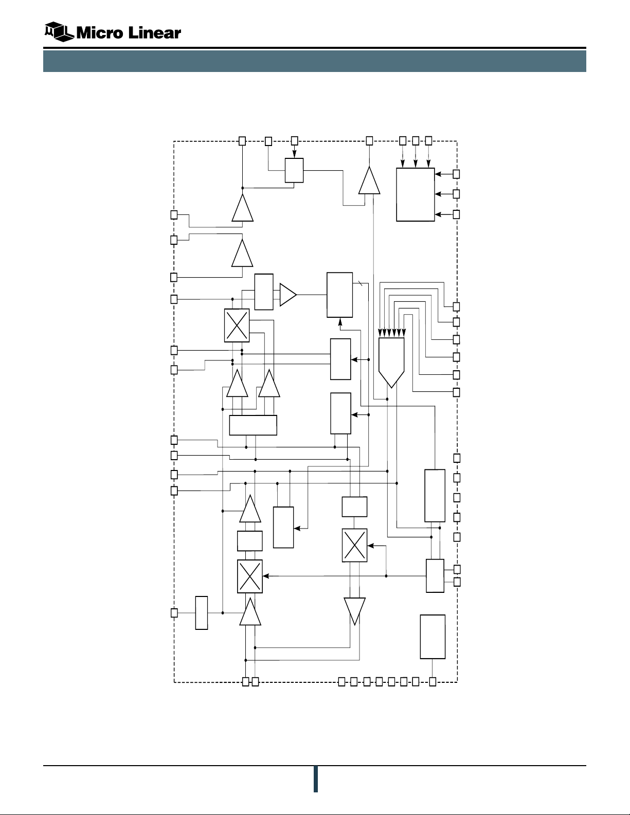
The ML2713 combined with the ML2712 forms an
FSK (Frequency Shift Keying) 2.4 GHz radio chipset
for systems based on IEEE802.11 and other wireless
communication protocols using the 2.4HGz ISM band.
The ML2713 is the complete IF section of Micro Linear’s
2.4GHz frequency hopping, half duplex radio transceiver
chipset. The chip’s down conversion super-heterodyne
receiver circuit contains an image reject down-convert
mixer, a limiter, a discriminator, a receive data filter and
a tracking A/D converter. The chips transmit circuit
contain a 6 bit D/A converter to digitally modulate the IF,
an anti alias filter and an image reject up-convert mixer.
APPLICATIONS
n 2.4GHz FSK radios
n PC Card and FlashCard Wireless Transceivers
n Systems based on IEEE802.11 1Mbps and 2Mbps
Standard
n TDMA Radio IF circuits
FEATURES
n Highly integrated IF transceiver
n Data rates up to 4Mbps
n Integrated discriminator and filter alignment circuits
n High signal to noise ratio at the discriminator output
n Received signal strength indicator (RSSI)
n D/A Converter for digitally generated IF
n Low sleep mode current - typically less than 1mA
n 3.0V to 5.5V operation
n Fast 10msec switch time between transmit and receive
modes
n 48 Pin TQFP, 7mm body
SIMPLIFIED BLOCK DIAGRAM
1
3
7
2
L
M
s
ia
B
r
lle
tro
n
o
C
T
n
a
i
r
t
s
m
P
o
w
r
e
p
A
m
l
i
f
i
r
e
.
R
C
.
o
L
o
p
F
i
l
t
r
e
ML2712
Tx Regulator
Output
2
o
L
O
L
o
p
F
i
l
t
&
r
e
T
n
a
k
C
u
c
i
r
i
t
1
o
L
O
L
o
p
F
i
l
t
&
r
e
T
n
a
k
C
u
c
i
r
i
t
3
2
M
C
l
o
2LO
Input
j
e
e
g
a
t
c
R
e
I
x
m
R
I
F
D
o
w
n
o
c
n
t
r
e
v
r
e
3
1
7
2
L
M
j
e
e
g
a
t
c
R
e
I
m
T
x
I
F
U
p
o
c
n
t
r
e
v
r
D
e
R
e
C
g
(e
n
e
f
e
e
r
c
R
e
q
e
F
r
u
n
e
c
y
I
n
p
u
t
H
z
c
k
D
RSSI
Limiter
A
C
o
n
C
c
i
r
C
o
n
o
t
r
l
I
n
f
e
c
t
a
r
e
d
n
a
b
se
a
B
r
lle
tro
n
o
C
., M
.g
i
i
m
s
r
c
i
n
t
a
o
r
u
d
Q
a
&
F
i
l
t
r
e
u
t
o
A
l
i
g
o
t
r
l
u
i
t
s
)
B
0
3
7
7
M
S
-
D
t
a
a
F
i
l
t
r
e
n
D
A
C
D
/
A
I
n
p
u
t
3
6
D
C
s
e
t
R
o
e
r
u
x
R
O
t
+
–
PRELIMINARY DATASHEET
January, 2000
Page 2

PRELIMINARY
ML2713
TABLE OF CONTENTS
General Description ................................................................................................................................................... 1
Applications ............................................................................................................................................................... 1
Features...................................................................................................................................................................... 1
Simplified Block Diagram .......................................................................................................................................... 1
Block Diagram ........................................................................................................................................................... 3
Pin Configuration ....................................................................................................................................................... 4
Pin Descriptions ......................................................................................................................................................... 4
Functional Description ............................................................................................................................................... 7
Introduction.............................................................................................................................................................. 7
Operational Modes .................................................................................................................................................. 8
Mode Control ........................................................................................................................................................... 8
Filter Align Mode..................................................................................................................................................... 8
Receive Mode ......................................................................................................................................................... 12
Sleep Mode.............................................................................................................................................................. 14
Test Mode Control .................................................................................................................................................... 14
Absolute Maximum Ratings........................................................................................................................................ 15
Electrical Characteristics............................................................................................................................................ 15
Operating Conditions ................................................................................................................................................. 15
Physical Dimensions .................................................................................................................................................. 20
Ordering Information .................................................................................................................................................. 20
WARRANTY
Micro Linear makes no representations or warranties with respect to the accuracy, utility, or completeness
of the contents of this publication and reserves the right to make changes to specifications and product
descriptions at any time without notice. No license, express or implied, by estoppel or otherwise, to any
patents or other intellectual property rights is granted by this document. The circuits contained in this
document are offered as possible applications only. Particular uses or applications may invalidate some of
the specifications and/or product descriptions contained herein. The customer is urged to perform its own
engineering review before deciding on a particular application. Micro Linear assumes no liability
whatsoever, and disclaims any express or implied warranty, relating to sale and/or use of Micro Linear
products including liability or warranties relating to merchantability, fitness for a particular purpose, or
infringement of any intellectual property right. Micro Linear products are not designed for use in medical,
life saving, or life sustaining applications.
© Micro Linear 2000. is a registered trademark of Micro Linear Corporation. All other trademarks are the
property of their respective owners.
Products described herein may be covered by one or more of the following U.S. patents: 4,897,611;
4,964,026; 5,027,116; 5,281,862; 5,283,483; 5,418,502; 5,508,570; 5,510,727; 5,523,940; 5,546,017;
5,559,470; 5,565,761; 5,592,128; 5,594,376; 5,652,479; 5,661,427; 5,663,874; 5,672,959; 5,689,167;
5,714,897; 5,717,798; 5,742,151; 5,747,977; 5,754,012; 5,757,174; 5,767,653; 5,777,514; 5,793,168;
5,798,635; 5,804,950; 5,808,455; 5,811,999; 5,818,207; 5,818,669; 5,825,165; 5,825,223; 5,838,723;
5.844,378; 5,844,941. Japan: 2,598,946; 2,619,299; 2,704,176; 2,821,714. Other patents are pending.
2
PRELIMINARY DATASHEET
January, 2000
Page 3
BLOCK DIAGRAM
V
A
R
I
A
B
L
E
C
A
P
A
C
I
T
O
R
A
R
R
A
Y
1
I
F
1
I
F
B
3
2
R
E
G
R
e
c
e
i
v
e
I
m
a
g
e
R
e
j
e
c
t
D
o
w
n
-
C
o
n
v
e
r
t
M
i
x
e
r
T
X
V
C
O
R
E
G
U
L
A
T
O
R
0
/
9
0
R
S
S
I
0
/
9
0
C
O
N
T
R
O
L
0
/
9
0
2
2
2
L
O
2
3
2
L
O
B
R
S
S
I
1
7
B
P
I
B
P
O
1
9
B
P
I
B
2
0
B
P
O
B
D
F
I
1
D
I
S
C
O
V
D
C
4
4
4
3
D
F
O
1
D
F
O
2
D
F
I
2
4
1
3
7
M
S
3
3
1
M
S
2
4
5
M
S
1
D
D
2
D
D
3
D
D
4
D
D
5
D
D
1
D
D
0
1
4
T
S
4
6
S
L
I
C
E
1
5
L
O
E
1
3
R
S
8
C
M
O
2
6
2
7
4
0
4
2
D
P
S
D
P
S
B
3
4
3
5
2
9
3
0
6
B
I
T
D
A
C
3
2
1
4
7
4
5
G
N
D
1
8
2
8
3
9
1
6
9
G
N
D
G
N
D
G
N
D
G
N
D
6
V
C
C
1
7
V
C
C
1
2
1
V
C
C
2
2
4
V
C
C
2
2
5
V
C
C
2
1
0
V
C
C
3
3
3
V
C
C
4
3
8
D
C
R
E
C
F
R
E
Q
U
E
N
C
Y
D
I
V
I
D
E
R
V
A
R
I
A
B
L
E
C
A
P
A
C
I
T
O
R
A
R
R
A
Y
0
/
9
0
V
A
R
I
A
B
L
E
C
A
P
A
C
I
T
O
R
A
R
R
A
Y
L
O
W
P
A
S
S
F
I
L
T
E
R
C
o
m
p
a
r
a
t
o
r
7
-
B
i
t
U
p
/
D
o
w
n
C
O
U
N
T
E
R
U
n
i
t
y
G
a
i
n
O
p
A
m
p
U
n
i
t
y
G
a
i
n
O
p
A
m
p
D
i
s
c
r
i
m
i
n
a
t
o
r
C
o
m
p
a
r
a
t
o
r
L
i
m
i
t
e
r
L
i
m
i
t
e
r
L
i
m
i
t
e
r
R
x
I
/
P
A
m
p
l
i
f
i
e
r
T
x
O
/
P
A
m
p
l
i
f
i
e
r
T
r
a
n
s
m
i
t
I
m
a
g
e
R
e
j
e
c
t
U
p
-
C
o
n
v
e
r
t
M
i
x
e
r
7
PRELIMINARY
ML2713
January, 2000
PRELIMINARY DATASHEET
3
Page 4
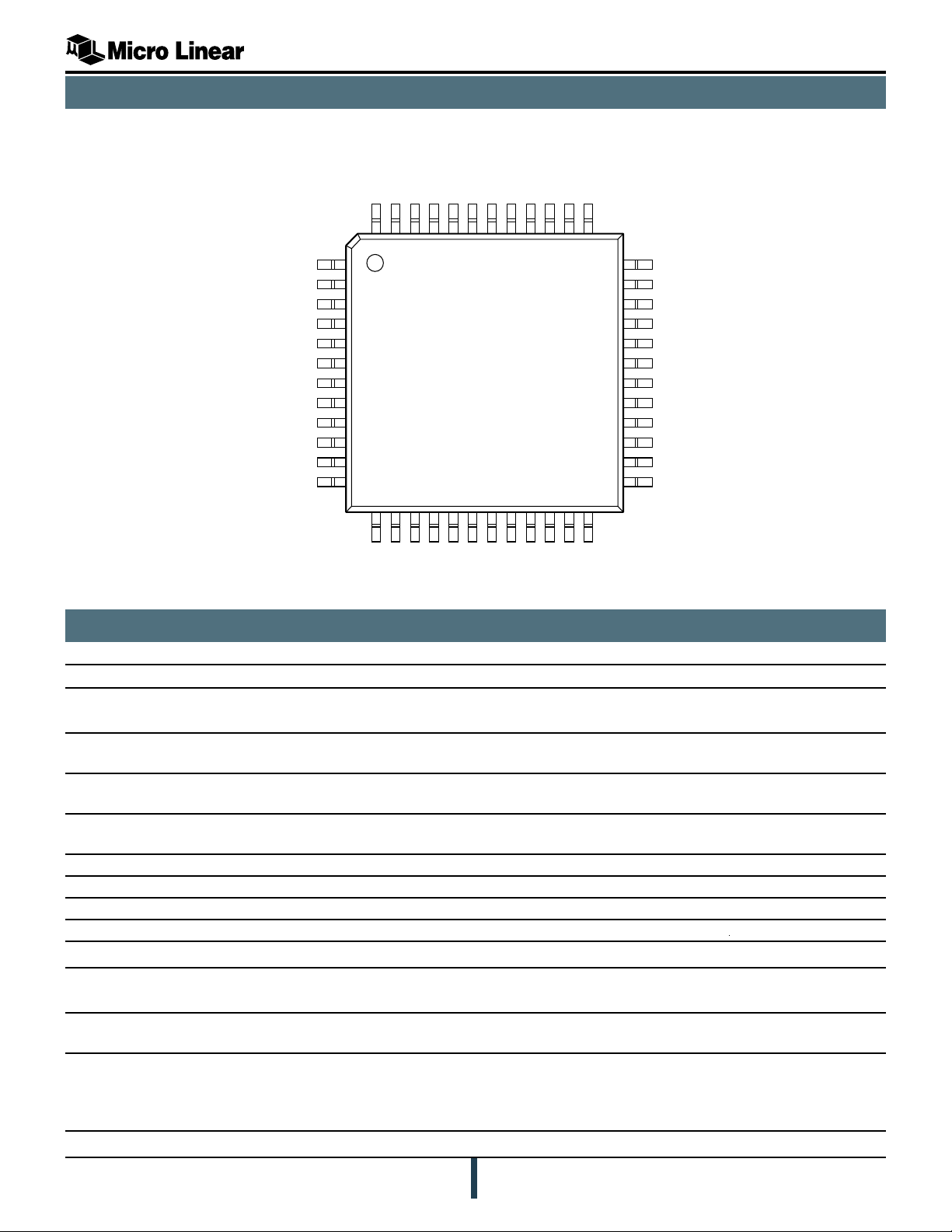
PIN CONFIGURATION
DD4
DD3
DD2
DD1
DD0
VCC1
VCC2
CMO
GND
VCC3
NC
NC
PRELIMINARY
ML2713
48-Pin TQFP (H48-7)
NC
DD5
SLICE
MS1
VDC
DFO2
DFI2
DFO1
DFI1
GND
48 47 46 45 44 43 42 41 40 39 38 37
1
2
3
4
5
6
7
8
9
10
11
12
13 14 15
18 19 20 21 22 23 24
16 17
DISCO
MS3
36
35
34
33
32
31
30
29
28
27
26
25
ML2713
NC
DPS
DPSB
VCC4
REG
MS2
BPO
BPOB
GND
1IF
1IF
VCC2
TS
RS
LOE
GND
RSSI
GND
BPI
BPIB
VCC2
2LO
LON2
VCC2
TOP VIEW
PIN DESCRIPTIONS
Pin # Signal Name I/O Type Description
POWER AND GROUND
6, 7 VCC1 POWER Voltage supply for digital I/O circuits. VCC1 should be greater than or
equal to VCC2, VCC3, and VCC4 in normal operation
21, 24, 25 VCC2 POWER Voltage supply for receive image reject down-converter and transmit
image reject up-converter
10 VCC3 POWER Voltage supply for D/A converter, comparator, mode control, and
alignment circuits
33 VCC4 POWER Voltage supply for limiters, discriminator, data filter, and transmit
regulator
9 GND GND Ground for VCC1
18, 28 GND GND Ground for VCC2
16 GND GND Ground for VCC3
39 GND GND Ground for VCC4
CONTROL
13 RS I (CMOS) Receive mode enable. This CMOS input is referenced to VCC1 and has
an on-chip pull-up. See Table 1 for operation
14 TS I (CMOS) Transmit mode enable. This CMOS input is referenced to VCC1 and has
an on-chip pull-up. See Table 1 for operation.
15 LOE I (CMOS) Chip enable and filter align control. This CMOS input is referenced to
VCC1 and has an on-chip pull up. The pin must be low for the IC to
operate in either transmit, receive or align modes. See Table 1 for
operation
4
PRELIMINARY DATASHEET
January, 2000
Page 5

PRELIMINARY
ML2713
PIN DESCRIPTIONS (CONTINUED)
Pin # Signal Name I/O Type Description
CONTROL (continued)
45 MS1 MODE SELECT Auto filter alignment disable. Tie to VCC4 to disable the on-chip filter
alignment. Tie to ground for normal operation
31 MS2 MODE SELECT Receive A/D converter disable. Tie MS2 to VCC2 to disable the on-chip
comparator and D/A converter in the receive mode. The D/A will still
be enabled in the transmit mode. Tie to ground for normal operation
37 MS3 MODE SELECT Test mode control pin. Tie this pin to ground at all times
RECEIVE
8 CMO O (CMOS) Comparator output. Active in receive mode, this CMOS output that is
referenced to VCC1 and has a nominal drive capability of 10mA
17 RSSI O(ANLG) Receive Signal Strength Indicator. This output has a nominal 1Volt
range. The RSSI voltage decreases with increasing received signal
level. The RSSI output has a 10k source impedance. It is referred to
VCC2
46 SLICE I(CMOS) DC time constant restore control. This input controls whether VDC is in
the hold or acquire mode. A high on this pin puts VDC in the acquire
mode, low puts VDC in the hold mode. This CMOS input is referred to
VCC1
RECEIVE AND TRANSMIT
47 DD5 I (CMOS) Six data inputs to Digital to Analog Converter. Inputs are not latched.
DD5 is the most significant bit (MSB).
1 DD4 I (CMOS) DD4
2 DD3 I (CMOS) DD3
3 DD2 I (CMOS) DD2
4 DD1 I (CMOS) DD1
5 DD0 I (CMOS) DD0 is the least significant bit (LSB)
22 2LO
23 2LOB I(ANLG) 2LO input. These pins are connected to a differential input stage that is
connected in a common base configuration. A pull-down resistor with a
nominal value of 4k is required on each pin to bias this input. The pull
down resistors are included on the ML2712 and do not need to be added
if that chip is used. The nominal differential input impedance is 200W
26 1IF
27 1IFB I/O(ANLG) Receive 1IF input and transmit 2IF output. These pins are bi-directional
I/O are connected to the receive input amplifier and transmit output
amplifier. These pins have a nominal differential impedance of 340W
set by on-chip resistances
TRANSMIT
32 REG O (ANLG) Transmit regulator output. This output of the on-chip regulator is
enabled in transmit mode. The nominal output voltage of the regulator
is 2.8V and drives current up to 25mA. The pin requires a de-coupling
capacitor with a nominal value 100nF
FILTERS - RECEIVE
35 DPS
34 DPSB ANLG Discriminator phase shift. These pins connect to the external
discriminator phase shift filter. These pins have a nominal differential
impedance of 600W set by on-chip resistors
January, 2000
PRELIMINARY DATASHEET
5
Page 6

PRELIMINARY
ML2713
PIN DESCRIPTIONS (CONTINUED)
Pin # Signal Name I/O Type Description
FILTERS - RECEIVE (continued)
38 DISCO O (ANLG) Discriminator voltage output. This emitter follower provides a nominal
drive capability of 100mA and a 200W source impedance
40 DFI1 I (ANLG) Stage 1 data filter input. Two on-chip operational amplifiers, Stage 1
and Stage 2, can be configured to make a 5th order filter with the use of
external resistors and capacitors
41 DFO1 O(ANLG) Stage 1 data filter output. The nominal output drive capability is
100mA
42 DFI2 I (ANLG) Stage 2 data filter input
43 DFO2 O (ANLG) Stage 2 data filter output. The nominal output drive capability is 100mA
44 VDC I/O (ANLG) DC time constant restore. An external capacitor sets the acquisition
time constant of the DC receiver restoration circuits that feed the on-
chip receive comparator. In the acquisition mode the nominal
impedance is 15kW. In hold mode the impedance is much higher, with
a nominal leakage current less than 2nA. The SLICE input determines if
VDC is in hold mode or in acquisition mode. This circuit ensures that
the received signal is centered on the on-chip D/A converter by
removing DC drift and transmitter and receiver frequency errors
FILTERS – TRANSMIT AND RECEIVE
19 BPI
20 BPIB I(FLTR) 2IF filter input. These pins connect to the receive image reject down-
convert mixer in the receive mode, to the 6-bit D/A converter in the
transmit mode, and to the 2LO input in the filter align mode. These
pins have a nominal differential impedance of 450 ohms set by on-chip
resistances
29 BPOB O(FLTR) 2IF filter output. These pins connect to the discriminator 0/90 phase
shift circuit in the receive mode and alignment modes, and the transmit
image reject up-convert mixer in the transmit mode
30 BPO
NON-CONNNECTED PINS
11, 12, 36, 48 NC No connect These pins should be left open
6
PRELIMINARY DATASHEET
January, 2000
Page 7

FUNCTIONAL DESCRIPTION
PRELIMINARY
ML2713
INTRODUCTION
The ML2713 is the complete IF section of Micro Linear's
2.4GHz frequency hopping, half duplex transceiver
chipset. The down conversion super-heterodyne receiver
circuits contain an image reject down-convert mixer, a
limiter, a discriminator, a receive data filter and a
tracking A/D converter. The transmit circuits contain a 6bit D/A converter to digitally generate the IF, an anti alias
filter and an image reject up-convert mixer. When
combined with the ML2712 it enables design of high
performance 2.4GHz half duplex radios with a fast
switching time between receive and transmit modes. This
is ideal for applications such as frequency hopping radios
based on the IEEE 802.11 FH standard.
The ML2713 has four modes of operation; 1) Filter Align,
2) Transmit, 3) Receive, and 4) Sleep. The operating
modes of the ML2713 can be programmed through a 3 pin
parallel interface.
The ML2713 has three filters; the 2IF, discriminator, and
data. Part of each filter is off chip, made up of external
components, and part is on chip. The 2IF and
discriminator filters have external inductors and
capacitors configured to give a bandpass characteristic.
In the Filter Align mode the ML2713 will adjust an on
chip capacitor array that is in parallel with the external
capacitance to correct for any tolerances in the external
components values, thereby centering the bandpass filters
to the correct frequency. In this way any production
trimming of the filters is eliminated. The data filter is
made up of on chip op-amps and off chip resistors and
capacitors and does not need to be aligned or trimmed.
In the Filter Align mode the ML2712 provides an 8MHz
signal to the 2LO port of the ML2713. The 2IF filter will
remove the fundamental of this signal, and pass the third
harmonic at 24Mhz to the limiter and discriminator. This
24MHz should result in a zero signal at the discriminator
output. If it does not, the alignment circuit will adjust the
on chip capacitor array until a zero signal is achieved.
In the Transmit mode, the ML2712 drives the 2LO port at
236MHz, and the 6-bit D/A converter is driven by a
digitally generated FSK modulated signal from the
baseband chip. Digital generation ensures that the
transmit modulation can be maximized without concern
for variations over temperature and process that result
from varying a VCO frequency directly. The D/A is
typically driven at 32 MHz, and the fundamental
component is 8MHz. The output of the D/A is connected
to the 2IF filter (which is acting as an anti alias filter)
where the 1st alias, which is 32MHz minus 8MHz or
24MHz, is passed. In this way the frequency of the
digitally generated transmit IF is normally designed to
equal the received 2IF, as will be described below. (This
radio architecture allows for a fast receive-to-transmit
switching speed, as no PLLs require re-tuning.) The output
of the 2IF filter is connected to the transmit image reject
up-convert mixer. This output mixes with the 2LO port
236MHz signal, and produces a 260MHz IF signal, which
is sent to the ML2712. In addition, the transmit signal is
passed through the SAW filter, which acts to select the
wanted alias, remove the unwanted up conversion
products, and perform part or all of the modulation filter
functions.
In the Receive mode, the ML2712 (in typical
applications) drives a 1IF signal of 260MHz through the
SAW filter and into the ML2713's 1IF port, and provides
the same 236MHz signal to the 2LO input as above. The
1IF port gains up the signal to improve the noise figure,
and sends the 1IF signal to the image reject down-convert
mixer. The mixer produces a 260MHz minus 236MHz or
24MHz 2IF signal which is then filtered by the 2IF filter.
This signal is gained up by the limiter stage, and sent to
the discriminator. The discriminator will convert changes
in the 2IF signal into a time varying signal which is then
filtered by the data filter. Increases in the 2IF result in
increasing voltage at the data filter output. The data filter
in turn drives one input of the output comparator. The
other input of the comparator is driven by the 6-bit D/A
converter. If the output of the D/A converter is lower than
the output of the data filter, the comparator output will
drive high. If the output of the D/A converter is higher
than the output of the data filter, the comparator output
will drive low. In this way a tracking A/D whose outputs
are the inputs to the D/A, and which follows the data
filter output, is implemented.
The offset errors of a transmitting source may be removed
by a receiving ML2713 during preamble. During
preamble, the Vdc capacitor can be put in the acquire
mode, and the average level of the data filter output will
appear across it. Once Vdc is put in the hold mode, and
data begins, all levels out of the data filtered are
referenced to the Vdc voltage, thereby removing any
offsets in the data.
In the Sleep mode, all circuits are powered off and the
chip typically draws less than 1mA.
January, 2000
PRELIMINARY DATASHEET
7
Page 8

OPERATIONAL MODES
PRELIMINARY
ML2713
MODE CONTROL
The ML2713 has four modes of operation; 1) Filer Align,
2) Transmit, 3) Receive, and 4) Sleep. The operating
modes of the ML2713 are programmed through the
parallel interface made up of pins RS, TS, and LOE. These
pins dynamically control the mode, and will enable the
appropriate circuitry within 1msec of transitioning low.
These control pins have on chip pull ups to VCC1, and are
CMOS compatible. The relationship between the
operating modes and control pins is shown in Table 1.
SRSTEOLnoitarepOfoedoM
hgiHhgiHhgiHedoMpeelS
ngilAretliF
hgiHhgiHwoL
nOtnemngilA
woLhgiHwoLedoMevieceR
hgiHwoLwoLedoMtimsnarT
Table 1. Mode Control Logic
stiucriCrevieceRemoS
retliFotuA,delbanE
FILTER ALIGN MODE
The ML2713 has three filters; the 2IF, discriminator, and
data. Part of each filter is off chip, made up of external
components, and part is on chip. The 2IF and
discriminator filters have external inductors and
capacitors configured to give a bandpass characteristic.
In the Filter Align mode the ML2713 will adjust an on
chip capacitor array that is in parallel with the external
capacitance to correct for any tolerances in the external
components values, thereby centering the bandpass filters
to the correct frequency. In this way any production
trimming of the filters is eliminated. The data filter is
made up of on chip op-amps and off chip resistors and
capacitors and does not need to be aligned or trimmed.
The Filter Align mode can be disabled by tying MS1 to
VCC4.
In the Filter Align mode the ML2712 provides an 8MHz
signal to the 2LO port, pins 2LO and 2LOB, of the
ML2713. The 2LO port is a low impedance common
base stage such that the 2LO signal is not attenuated by
the parasitic capacitance of the ML2712, ML2713, the
interconnect between them, and their packages. The 2LO
port then drives the 2IF filter, and a frequency divider. The
frequency divider divides the 8MHz signal down to a
500kHz which then clocks a 7-bit up/down counter. The
2IF filter will remove the fundamental of this signal, and
pass the third harmonic at 24Mhz through a 0/90 degree
phase splitter to the limiters which in turn drive the
discriminator. The output of the discriminator connects to
a low pass filter, which then drives a comparator. This
comparator looks to see if the discriminator output is
greater than or less than zero volts differential. If the
discriminator filter bandpass characteristic is centered
properly on 24MHz, then the 24MHz input to the
discriminator should result in a zero signal at the
discriminator output. If the center frequency is too high,
the discriminator output will go high. If the center
frequency is too low, the discriminator output will go low.
A high or a low here will signal the up/down counter to
increment or decrement respectively. The up/down
counter then drives three identical variable capacitor
arrays, leading to changes in on chip capacitors. Two of
these on chip capacitors are in parallel with off chip
capacitors in the 2IF filter, and one is in parallel with the
off chip capacitor in the discriminator filter. These will
cancel any tolerance associated with the off chip
components such that the center frequencies of both
filters are properly centered. The 7 bit up/down counter
begins at mid code of 128 levels, so there will be a
maximum of 64 counts in either direction. Since the up/
down counter is clocked at the 500kHz frequency, the
filters will align within 128msec. Therefore, in a WLAN
system, the filters can be re-aligned every time the radio
hops to a new frequency because it can do so in less time
than it takes for the PLLs to settle. When switching from
Filter Align mode, the up/down counter freezes, keeping
the 7-bit result of the alignment fixed. Whenever the
ML2713 is put in the Sleep mode, the up/down counter
resets to the mid point. Therefore, if the Filter Align is
being used, the filters must be realigned prior to receiving
or transmitting.
Active circuits in Filter Align Mode are shown in Figure
1.
8
PRELIMINARY DATASHEET
January, 2000
Page 9

PRELIMINARY
OPERATIONAL MODES (CONTINUED)
BPI BPO
RSSI
17
RSSI
BPIB20BPOB
19
ML2713
DPSDPSB
34 352930
DISCO
38
DFI1
40
DFO1
41
DFI2
42
1IF
1IFB
VCC1
VCC1
VCC2
VCC2
VCC2
VCC3
VCC4
Limiter
Receive Image Reject
Down-Convert Mixer
26
27
Rx I/P
Amplifier
Tx O/P
6
7
21
24
25
10
33
Amplifier
0/90
Limiter
VARIABLE
CAPACITOR
ARRAY
Transmit Image Reject
Up-Convert Mixer
0/90
0/90
VARIABLE
CAPACITOR
ARRAY
Limiter
Discriminator
VARIABLE
CAPACITOR
ARRAY
6 BIT
DAC
LOWPASS
Comparator
Up/Down
COUNTER
FILTER
7 -Bit
Unity Gain
Op Amp
7
Unity Gain
Op Amp
Comparator
CONTROL
D C
REC
43
DFO2
44
VDC
46
SLICE
8
CMO
14
TS
15
LOE
REG
32
TX VCO
REGULATOR
0/90
22
2LO232LOB
GND
FREQUENCY
DIVIDER
3 2 1 4745
DD2 DD3 DD4 DD5DD1DD0
GND
18 28 39169
GND
GND
GND
Figure 1: Circuits Active in Filter Align Mode
January, 2000
PRELIMINARY DATASHEET
45
MS1
31
MS2
37
MS3
13
RS
9
Page 10

PRELIMINARY
OPERATIONAL MODES (CONTINUED)
ML2713
TRANSMIT MODE
The transmitter is a Frequency Shift Key (FSK) transmitter
in which the modulating signal is a digitally generated
signal from the baseband chip. This signal in turn is
passed through an anti alias filter, and mixed with an LO
signal to produce a 260MHz 2IF signal which is then
passed to the ML2712. The digitally generated 1st If is
designed to be equal to the received 2IF. Such a radio
architecture allows for rapid switching between receive
and transmit modes because the PLLs and filters don't
need to be re-tuned or aligned with each mode switch.
In the Transmit mode, the ML2712 drives the 2LO port at
236MHz, and the 6-bit D/A converter pins DD5-DD0 are
driven by a digitally generated FSK modulated signal
from the baseband chip. Digital generation ensures that
the transmit modulation can be maximized without
concern for variations over temperature and process that
result from varying a VCO frequency directly. The D/A is
typically driven at 32 MHz, and the fundamental
component is 8MHz. The output of the D/A is connected
to the 2IF filter (which is acting as an anti alias filter)
where the 1st alias, which is 32MHz minus 8MHz or
24MHz, is passed. The 2IF filter connects to a 0/90
degree phase splitter, which in turn connects to the
transmit image reject up-convert mixer. The 2LO port
connects to a 0/90 degree phase splitter, which in turn
drives the other input of up-convert mixer. This phase
splitter output mixes with the 2LO port 236MHz signal,
and produces a 260MHz IF signal, which is sent to the
ML2712. In addition, the transmit signal is passed
through the SAW filter, which acts to select the wanted
alias, remove the unwanted up conversion products, and
perform part or all of the modulation filter functions.
Transmitter Circuits
The main circuits active during the transmit mode are:
2IF of 24MHz. Under these conditions, the image
rejection is typically better than 25dB. This is shown in
Figure 2. The fundamental, at 260MHz, is at least 25dB
greater than the image. The products at 8MHz intervals
are unwanted aliases from the D/A converter.
The differential 2LO input port has a nominal 200-Ohm
impedance. The 2LO port is a low impedance common
base stage such that the 2LO signal is not attenuated by
the parasitic capacitance of the ML2712, ML2713, the
interconnect between them, and their packages. Each
input requires external pull down resistors of 4k to
properly bias them. These resistors are internal to the
ML2712, and do not need to be included if that device is
used.
0
-10
-20
-30
-40
Power into 50W (dBm)
-50
-60
-70
160 180 200 220 240 260 280 300 320 340 360
Fr equency ( MHz)
Figure 2. Typical Transmit Output Spectrum
Dat a
Mar ke r 1
Mar ke r 2
6-bit D/A Converter
The D/A converter on the ML2713 is a parallel interface,
binary weighted D/A converter, with non-latched CMOS
compatible inputs. The D/A can be driven at frequencies
up to 40MHz.
2IF Filter
The 2IF filter is an off chip inductor and capacitor filter
which is shared between the receive and transmit
circuits.
IF Up-Converter
The image reject transmit mixer consists of a 2IF input 0/
90 degree splitter, 2LO input buffer a 2LO 0/90 degree
splitter, two mixers and an output combiner. The 0/90
degree networks are passive and internal to the IC. The
mixer performs optimally with a 1IF of 260MHz, and a
10
PRELIMINARY DATASHEET
January, 2000
Page 11

PRELIMINARY
OPERATIONAL MODES (CONTINUED)
Transmit Output Buffer
ML2713
The transmit output buffer is a limiting amplifier. Its
nominal output power at 260MHz is -12dBm, driving
a 340W differential load.
On IC Transmit Regulator
which is enabled and disabled with the transmit circuits.
The regulator powers external circuits such as a transmit
VCO. The noise floor of the ML2713 is shown in the
Figure 3. The regulator minimizes noise output above
5KHz to avoid introducing phase noise into the VCO.
The transmitter circuits in the ML2713 are shown in Figure
4.
BPI BPO
RSSI
17
RSSI
BPIB20BPOB
19
100000
10000
1000
100
PSD (nVrms/rtHz)
10
100 1000 10000 100000 1000000 10000000
Figure 3. Transmit Regulator Noise Floor
DPSDPSB
34 352930
DISCO
38
Frequency (Hz)
DFI1
DFO1
40
41
DFI2
42
1IFB
VCC1
VCC1
VCC2
VCC2
VCC2
VCC3
VCC4
REG
VARIABLE
CAPACITOR
ARRAY
6 BIT
DAC
3 2 1 4745
DD2 DD3 DD4 DD5DD1DD0
Discriminator
Comparator
LOWPASS
FILTER
7 -Bit
Up/Down
COUNTER
7
Unity Gain
Op Amp
Unity Gain
CONTROL
31
45
MS1
Op Amp
Comparator
MS2
43
DFO2
44
VDC
D C
46
REC
37
MS3
SLICE
8
CMO
14
TS
15
LOE
13
RS
0/90
VARIABLE
CAPACITOR
ARRAY
Limiter
Limiter
Receive Image Reject
Down-Convert Mixer
26
1IF
27
6
7
21
24
25
10
33
32
TX VCO
REGULATOR
Rx I/P
Amplifier
Tx O/P
Amplifier
22
2LO232LOB
0/90
VARIABLE
CAPACITOR
Transmit Image Reject
Up-Convert Mixer
0/90
GND
ARRAY
Limiter
0/90
FREQUENCY
DIVIDER
GND
18 28 39169
GND
GND
GND
Figure 4. Circuits Active in Transmit Mode
January, 2000
PRELIMINARY DATASHEET
11
Page 12

PRELIMINARY
OPERATIONAL MODES (CONTINUED)
ML2713
RECEIVE MODE
The receiver on the ML2713 is a single conversion,
superheterodyne receiver with on chip A/D conversion.
Input signals from the ML2712 are down converted from
260MHz to 24MHz, filtered, limited, and then converted
to DC voltages by the discriminator. A tracking A/D then
converts the filtered discriminator output into a 6-bit
digital word.
In the Receive mode, the ML2712 (in typical
applications) drives a 1IF signal of 260MHz through the
SAW filter and into the ML2713's 1IF port, and provides
the same 236MHz signal to the 2LO input as above. The
1IF port gains up the signal to improve the noise figure,
and sends the 1IF signal to the image reject down-convert
mixer. The 2LO port drives a 0/90 degree phase splitter
whose output is connected the down-convert mixer. The
mixer produces a 260MHz minus 236MHz or 24MHz 2IF
signal which is then filtered by the 2IF filter. The output
of the 2IF filter passes through another 0/90-degree phase
splitter, and is gained up by the limiter stages, and sent to
the discriminator. The discriminator will convert changes
in the 2IF signal into a time varying signal, which is then
filtered by the data filter. Increases in the 2IF result in
RSSI
17
BPI BPO
BPIB
19
20
BPOB
increasing voltage at the data filter output. The data filter
in turn drives one input of the output comparator. The
other input of the comparator is driven by the 6-bit D/A
converter. If the output of the D/A converter is lower than
the output of the data filter, the comparator output will
drive high. If the output of the D/A converter is higher
than the output of the data filter, the comparator output
will drive low. The comparator output then drives an
external up/down counter, counting up when the
comparator output is high, and counting down when it is
low. The outputs of the up/down counter can then drive
the input of the 6-bit D/A converter. In this way a
tracking A/D whose outputs are the inputs to the D/A, and
which follows the data filter output, is implemented. This
circuit samples at a rate of up to 20MHz, and yields a 5bit digitization of the signal.
The offset errors of a transmitting source may be removed
by a receiving ML2713 during preamble. During
preamble, the Vdc capacitor can be put in the acquire
mode, and the average level of the data filter output will
appear across it. Once Vdc is put in the hold mode, and
data begins, all levels out of the data filtered are
referenced to the Vdc voltage, thereby removing any
offsets in the data. An external capacitor connected to
VDC sets the acquire time constant.
DPSDPSB
34 352930
DISCO
38
DFI1
40
DFO1
41
DFI2
42
1IFB
VCC1
VCC1
VCC2
VCC2
VCC2
VCC3
VCC4
REG
RSSI
VARIABLE
ARRAY
6 BIT
DAC
3 2 1 4745
DD2 DD3 DD4 DD5DD1DD0
Discriminator
Comparator
LOWPASS
FILTER
7-Bit
Up/Down
COUNTER
7
Unity Gain
Op Amp
Unity Gain
CONTROL
45
MS1
Op Amp
Comparator
31
MS2
37
D C
REC
MS3
43
DFO2
44
VDC
46
SLICE
8
CMO
14
TS
15
LOE
13
RS
ARRAY
Limiter
Limiter
CAPACITOR
Receive Image Reject
Down-Convert Mixer
26
1IF
27
Rx I/P
Amplifier
Tx O/P
TX VCO
REGULATOR
Amplifier
0/90
22
2LO232LOB
6
7
21
24
25
10
33
32
0/90
VARIABLE
CAPACITOR
ARRAY
Transmit Image Reject
Up-Convert Mixer
GND
Limiter
0/90
FREQUENCY
GND
DIVIDER
18 28 39169
GND
GND
GND
0/90
VARIABLE
CAPACITOR
12
Figure 5. Circuits Active in Receive Mode
PRELIMINARY DATASHEET
January, 2000
Page 13

PRELIMINARY
OPERATIONAL MODES (CONTINUED)
ML2713
RECEIVER CIRCUITS
The main circuits active in the receive mode are:
Image Reject Receive Mixer
The image reject receive mixer consists of an input
splitter, a 2LO input buffer, a 0/90 degree splitter, two
mixers and a 0/90 degree IF combiner. The 0/90 degree
networks are passive and internal to the IC. The design of
the mixer is centered to give optimum performance with
a 260MHz 1IF, 24MHz 2IF. Under these conditions the
image rejection is typically better than 25dB.
The differential 2LO input port has a nominal 200W
impedance. The 2LO port is a low impedance common
base stage such that the 2LO signal is not attenuated by
the parasitic capacitance of the ML2712, ML2713, the
interconnect between them, and their packages. Each
input requires external pull down resistors of 4k to
properly bias them. These resistors are internal to the
ML2712, and do not need to be included if that device is
used.
2IF FILTER
The 2IF filter requires two external inductors and four
external capacitors. This circuit is differential to minimize
noise pick up in the 2IF circuit. This filter is auto aligned
and is slaved to the discriminator. The ML2713 has been
designed so that the same inductors and nearly the same
capacitors can be used in both the discriminator and filter.
It is recommended that the same inductors be used for the
two circuits and that they be co-located on a reel of
components. This will ensure minimal difference between
the inductor values so that the filter and discriminator
center frequencies are very similar, if not identical.
Discriminator Phase Shift
The discriminator performs the frequency to voltage
conversion. The 0/90 degree phase shift is internal, but
external components (one inductor and one capacitor) are
required for the differential phase shift versus frequency
(d/df). The center frequency of the d/df circuit is tuned by
a capacitor array during Align Mode. This capacitor array
has a nominal variation of 10pF, which for a 24MHz IF is
sufficient to cope with a 10% total component tolerance
(including temperature) in the external L and C (
e.g.
, 5%
capacitor & 5% inductor tolerance).
Receiver Data Filter
DC Restoration
The receiver is intended for use in TDMA radios. This
requires rapid turn on of circuits, then the ability to
remove the effect of DC offsets and the frequency offset
of any received signal.
DC restoration circuits on the ML2713 let the acquisition
time be controlled by the value of an external capacitor.
The DC restoration, during acquisition, forces the mean
input voltage of the comparator to equal the mid-range
voltage of the D/A. This is important as it minimizes the
number of bits required in the tracking A/D. This DC
restoration is achieved by estimating the mean level of
the receive data filter output voltage and subtracting the
difference between this and the D/A mid point. For small
errors a single pole internal resistor and external capacitor
is used to calculate the mean. When the error is large
(
e.g.
, when first enabling the receiver or at the start of a
TDMA packet) a fast charge circuit speeds acquisition.
Receive A/D
External digital circuits can be used to make a tracking
A/D converter by using the D/A and comparator. The
digital circuits try to force the A/D output to be the same
as the received signal input to the comparator. The digital
circuits require an up/down counter, which will drive the
D/A. This is shown in Figure 6.
+
–
6 BIT D/A
Figure 6. Tracking ADC Block Diagram
CMO
DD0 - DD5
COUNT
UP/DOWN
TO DEMODULATOR
When the receive signal at the comparator input voltage
is greater than the D/A output voltage (inverting input to
comparator), the comparator output (CMO) goes high,
which increments the digital counter, which in turn
increases the D/A output voltage. The circuit is clocked to
keep the D/A output tracking the received signal. If the
comparator output is low, then the counter decrements
and reduces the D/A output voltage. This means the
output of the D/A, or the counter output, is a digitized
version of the received signal. This is shown in Figure 7.
V
RECEIVED SIGNAL
D/A OUTPUT
The receiver data filter is made up of two on chip unity
gain op-amps, and off chip inductors and resistors
configured as a 5th order filter. This filter does not need to
be tuned or aligned.
January, 2000
Figure 7. Receive Tracking A/D Signals Illustrated
PRELIMINARY DATASHEET
CMO
SAMPLE
CLOCK
IN
COUNTER
TIME
13
Page 14

PRELIMINARY
OPERATIONAL MODES (CONTINUED)
ML2713
The D/A voltage (overlaid on the received signal) and the
CMO output are relative to the sample clock of the
external counter circuit. For some applications the counts
and D/A output can be incremented and decremented in
one LSB. However, if the rate of change of voltage is too
high, then two or more counts/LSB may needed to keep
track of the received signal. A typical application is
where the update rate of the tracking A/D is 16MHz.
RSSI
The Received Signal Strength Indicator (RSSI) is generated
by summing the signal measured in the 2IF limiter and
the 1IF amplifier. Inclusion of the 1IF amplifier in the
RSSI equation enables the maximum input level to be
higher than with normal IF superheterodyne receiver ICs.
The RSSI output is referenced to VCC2 and decreases with
increasing signal level. See Figure 8. The RSSI output is
compatible with the ML2712's RSSI A/D converter. The
rise and fall times are typically 4msec which is ideal for
performing clear channel assessment or preamble antenna
diversity in a WLAN system.
3.1
3.0
2.9
2.8
2.7
2.6
VOLTS (V)
2.5
2.4
2.3
2.2
2.1
–100 20
Figure 8. Typical RSSI Response with a 260MHz 1IF
–80
–60
–40
POWER (dBm)
–20
0
SLEEP MODE
When going into sleep mode all circuits are powered off
and the chip typically draws less than 1mA. Sleep mode
also resets the alignment up/down counter to its
midpoint.
Test Mode Control
MS1, MS2, and MS3 are CMOS logic inputs that activate
on chip test modes. For normal operation, ground all of
these pins. Each of these pins has a large value pull
down resistor to ground. Tying MS1 to VCC4 will disable
the Filter Align circuitry. Tying MS2 to VCC2 will disable
the Receive A/D converter by shutting off both the 6-bit
D/A converter and comparator in the receive mode. MS3
should remain tied to ground at all times.
14
PRELIMINARY DATASHEET
January, 2000
Page 15

PRELIMINARY
ML2713
ABSOLUTE MAXIMUM RATINGS
Absolute maximum ratings are those values beyond which
the device could be permanently damaged. Absolute
maximum ratings are stress ratings only and functional
device operation is not implied.
VCC1, VCC2 ............................................................ 6.0V
VCC3, VCC4, VCC5, VCC6, VCC7 . -0.3 TO VCC1 + 0.3V
GND .......................................................... -0.3V to 0.3V
Junction Temperature .............................................. 150ºC
Storage Temperature Range ...................... –65ºC to 150ºC
Lead Temperature (Soldering, 10s) .......................... 260ºC
OPERATING CONDITIONS
Commercial Temperature Range.................... 0ºC to 70ºC
Extended Temperature Range ..................... -20ºC to 70ºC
VCC Range ..................................................3.3V to 5.5V
Thermal Resistance (qJA) (Note 1) ...................... 100ºC/W
ELECTRICAL CHARACTERISTICS
Unless otherwise specified, VCC3, VCC4, VCC5, VCC6, VCC7 = 3.3V, VCC1, VCC = 5V, TA = Operating Temperature
Range (Note 1)
SYMBOL PARAMETER CONDITIONS MIN TYP MAX UNITS
POWER CONSUMPTION TX RF AND RX RF
All Circuits, Sleep Mode DC Connected 1 µA
Supply Current Filter Align Mode 30 mA
INTERFACE LOGIC LEVELS
Input High (The ML2713 has internal pullup VCC1 5.5 V
Output Low –0.4 VCC1 V
Input capacitance (not tested) 4 pF
MODE CONTROL PINS
Input High Connect to VCC1 VCC1 – 0.3 VCC1 V
Output Low Connect to GND GND GND +0.3 V
Input bias current All states –11mA
Filter Alignment Time From LOE asserted to aligned, 2IF 120 µs
Transmit Turn On Time Time from TR asserted to valid TX IF 2 µs
Receive Turn On Time From RS asserted to the ADC input 10 µs
Receive Mode 30 mA
Transmit Mode 23 mA
resistors to VCC1) ± 0.7
± 0.3
24MHz, 8MHz square wave cal
tone on 2LO input
signal at output
signal DC adjusted to the mid point
of the ADC. CW 260MHz signal
at –80dBm
January, 2000
PRELIMINARY DATASHEET
15
Page 16

PRELIMINARY
ML2713
ELECTRICAL CHARACTERISTICS (CONTINUED)
SYMBOL PARAMETER CONDITIONS MIN TYP MAX UNITS
RECEIVE COMPARATOR OUTPUT
Output High VCC1 – 0.5 V
Output Low 0.4 V
Output Sink/Source 10 mA
RECEIVER AC ELECTRICAL SPECIFICATION (Note 3)
F2IF 2IF Frequency Nominal, modulated 24 MHz
F1IF 1IF Frequency Nominal modulated 240 260 280 MHz
2LO 2LO Input Frequency 216 236 256 MHz
2LO Input Signal Level Differential 200W, with 2kW pull –23 dBm
down to GND on each pin
1IF Input Impedance Differential, 260MHz 340 W
2IF Input Impedance, IF Band Pass Filter Differential, 24MHz 450 W
Discriminator Phase Shift Circuit Differential, 24MHz 600 W
Input Noise Figure 7dB
Irreducible Error Rate (Note 4) 2Mb/s measured –60dBm 10
–5BER
Preamble Settling Time –80dBm Signal, with IEEE 802.11 FH 10 µs
3dB Modulation Bandwidth, from Input 260MHz IF input at –50dBm, mod- 500 700 kHz
to ADC Output (Note 5) ulation rate (2FSK h = 0.32) for 3dB
RSSI PERFORMANCE
RSSI Rise Time. Noise to –10dBm 20pF loading the RSSI output 4 10 µs
into the IF Mixer.
RSSI Fall Time, –10dBm to Noise 20pF loading the RSSI output 4 10 µs
into the IF Mixer.
RSSI Linearity Differential gradient from –84dBm 1.0 V
RSSI Maximum Voltage VCC1 V
RSSI Minimum Voltage No signal applied VCC1 – 1V
RSSI Sensitivity, Mid Range 7 10 13 mV/dB
RSSI Maximum Signal into IC The highest signal at which the –6 dBm
RSSI Minimum Signal into IC The lowest signal at which the –100 –85 dBm
preamble, to within 10% of mid
point
reduction in eye opening, compared
to 100kHz modulation.
to –15dBm
RSSI sensitivity is >50% nominal
for the IC
RSSI sensitivity is >50% nominal
16
PRELIMINARY DATASHEET
January, 2000
Page 17

PRELIMINARY
ML2713
ELECTRICAL CHARACTERISTICS (CONTINUED)
SYMBOL PARAMETER CONDITIONS MIN TYP MAX UNITS
TRANSMITTER AC ELECTRICAL SPECIFICATION (Continued)
Level of Image Frequency (2LO – F2IF) Relative to Transmit IF output –25 dBc
Product
Spurious Output Level (DC to 600MHz) Relative to Transmit IF output –25 dBc
2LO Breakthrough Relative to Transmit IF output –25 dBc
SNR of Transmit IF (Note 6) Measured over 1MHz bandwidth, 36 dB
centered on 260MHz. CW 24MHz
tone generated by DAC.
Relative Accuracy ±0.5 LSB
Output Settling Time To within 1LSB 10 ns
Signal to Noise and Distortion At 24MHz alias, 1MHz bandwidth 36 dB
TXVCO REGULATOR (Note 7)
Output voltage 2.6 2.8 3.1 V
Current 25 mA
RMS Output Noise, >6000Hz. 100 nV/ÖHz
PSRR 22 dB
Turn On Time To 90% of final voltage from 1 µs
transmit enable
Turn Off Time To 90% of final voltage from 2 µs
transmit enable
Note 1: Limits are guaranteed by 100% testing, sampling, or correlation with worst case test conditions.
Note 2: qJA is measured with the component mounted on the Evaluation PCB in free air.
Note 3: IF center frequency is 260MHz, 2IF center frequency is 24MHz, 2LO frequency is 236MHz.
Note 4: Irreducible error rate derived from eye opening using a 4FSK input signal and measuring SNR > 32dB post digitization.
Note 5: With recommended data filter component values.
Note 6: SNR measured over a 1MHz bandwidth using a CW 24MHz tone.
Note 7: 100nF decoupling capacitor required to ground.
January, 2000
PRELIMINARY DATASHEET
17
Page 18

PHYSICAL DIMENSIONS
0.354 BSC
(9.00 BSC)
0.276 BSC
(7.00 BSC)
1
PIN 1 ID
PRELIMINARY
Package: H48-7
48-Pin (7 x 7 x 1mm) TQFP
0º - 8º
37
ML2713
0.003 - 0.008
(0.09 - 0.20)
13
0.020 BSC
(0.50 BSC)
0.007 - 0.011
(0.17 - 0.27)
ORDERING INFORMATION
0.276 BSC
(7.00 BSC)
25
0.354 BSC
(9.00 BSC)
0.037 - 0.041
(0.95 - 1.05)
0.048 MAX
(1.20 MAX)
0.018 - 0.030
(0.45 - 0.75)
SEATING PLANE
18
PART NUMBER TEMPERATURE RANGE PACKAGE
ML2713CH 0°C to 70°C 48 Pin TQFP
ML2713EH -20°C to 70°C 48 Pin TQFP
Micro Linear Corporation
2092 Concourse Drive
San Jose, CA 95131
Tel: (408) 433-5200
Fax: (408) 432-0295
www.microlinear.com
PRELIMINARY DATASHEET
January, 2000
DS2713-01
 Loading...