

Page 1
July 2000
ML2652/ML2653
10Base-T Physical Interface Chip
GENERAL DESCRIPTION
The ML2652, 10BASE-T Physical Interface Chip, is a
complete physical interface for twisted pair and AUI
Ethernet applications. It combines a 10BASE-T MAU,
Manchester Encoder/Decoder, and Twisted Pair Interface
filters in one monolithic IC. A complete DTE interface for
twisted pair Ethernet can be implemented by combining
the ML2652, an Ethernet controller, and transformers.
The ML2652 can automatically select between an AUI and
twisted pair interface based on Link Pulses. Six LED
outputs provide complete status at the physical link. Link
pulse testing can be enabled or disabled through the
LTP LED Pin.
The unique transmitter design uses a waveform generator
and low pass filter to meet the 10BASE-T transmitter
requirements without the need for an external filter. The
differential current driven output reduces common mode
which in turn results in very low EMI and RFI noise.
The ML2652 and ML2653 (28 pin version) are implemented
in a low power double polysilicon CMOS technology. The
ML2653 does not include the AUI interface.
FEATURES
■ Complete physical interface solution
■ Conforms to IEEE 802.3i–1990 (10Base-T)
■ On-chip transmit and receive filters
■ Automatic AUI/Twisted Pair selection (ML2652 only)
■ Power down mode
■ Pin selectable controller interface-(CS0 – CS2)
Intel 82586, 82596
NSC DP8390
Seeq 8003, 8005
AMD 7990
■ Automatic polarity correction
■ Pin selectable receive squelch levels
■ Status pins for: link detect, receive &
transmit activity, collision, jabber, AUI selection
■ Single supply 5V ±5%
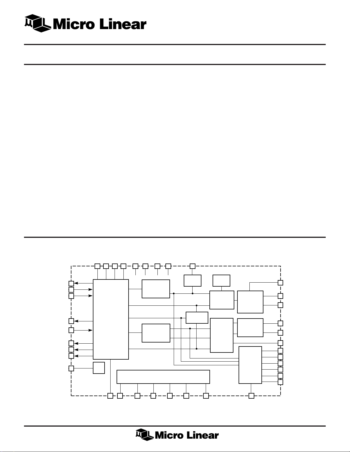
ML2652 BLOCK DIAGRAM
CS1 CS2 FD V
CS0
TxC
TxE
TxD
COL
LPBK
RxC
RxE
RxD
CLK
CONTROLLER
INTERFACE
OSC
RPOL
CCVCC
DATA
ENABLE
COLLISION
DATA
ENABLE
AUISEL RCVCLS
GND GND
MANCHESTER
ENCODER
MANCHESTER
DECODER
XMT
LEDS
JABDIS
JABBER
DETECT
COLLISION
DETECT
LTP JAB
LINK
PULSE
XMT
WAVEFORM
GEN & LPF
RECEIVER
CURRENT
DRIVEN XMT
OUTPUT
DRIVER
RECEIVE
LPF
AUI
AUI/TP
RTX
Tx+
Tx–
Rx+
Rx–
RSL
DO+
DO–
CI+
CI–
DI+
DI–
1
Page 2
ML2652/ML2653
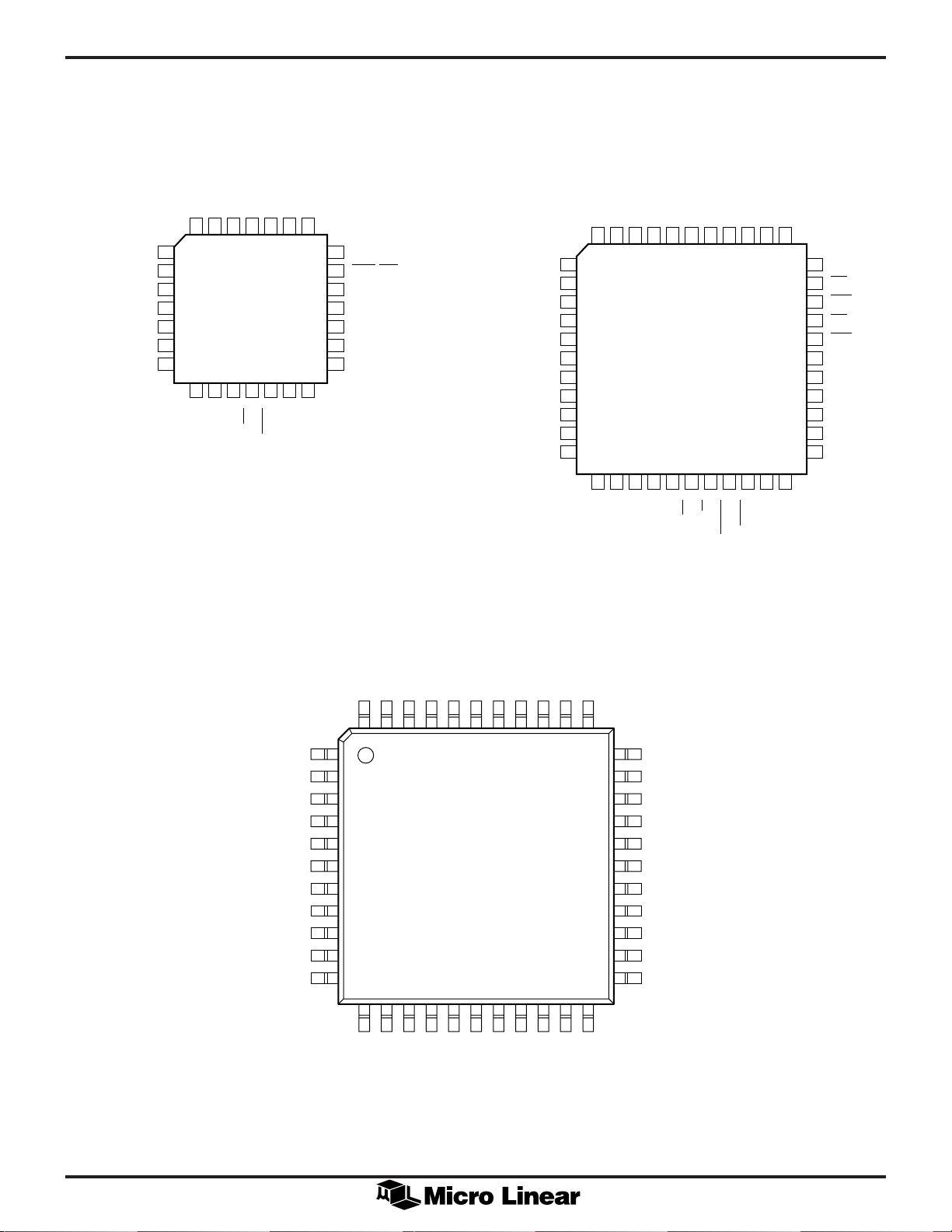
PIN CONNECTIONS
Tx–
NC
CLK
LPBK
Rx+
Rx–
NC
28-Pin PLCC (Q28)
GND
5
6
7
8
9
10
11
Tx+
4321282726
12 13 14 15 16 17 18
CCVCC
V
ML2653
GND
TxC
TxD
FD
LTP
RPOL
TxE
COL
RTX
CS0
25
24
23
22
21
20
19
RSL
XMT/RCV
RxD
RxC
RxE
CS2
CS1
DO+
DO–
CLK
LPBK
GND
Rx+
Rx–
NC
NC
DI+
DI–
ML2652
44-Pin PLCC (Q44)
NCNCTx–
6543214443424140
7
8
9
10
11
12
13
14
15
16
17
18 19 20 21 22 23 24 25 26 27 28
CI+
CI–
CCVCC
V
GND
Tx+
FD
GND
LTP
TxC
AUI/TP
TxD
AUISEL
TxE
RPOL
RTX
COL
JABDIS
CS0
RSL
39
JAB
38
XMT
37
CLS
36
RCV
35
RXD
34
RxC
33
RxE
32
CS2
31
CS1
30
GND
29
NC
NC
CLK
LPBK
NC
Rx+
Rx–
NC
NC
NC
NC
44-Pin TQFP (H44-10)
NCNCTx–
44 43 42 41 40
1
2
3
4
5
6
7
8
9
10
11
12 13 14 15 16
NC
NC
VCCV
ML2653
GND
Tx+
GND
TxC
39 381937203621352234
17 18
FD
CC
LTP
AUI/TP
TxD
NC
TxE
RPOL
RTX
COL
JABDIS
33
32
31
30
29
28
27
26
25
24
23
CS0
RSL
JAB
XMT
CLS
RCV
RXD
RxC
RxE
CS2
CS1
NC
2
Page 3
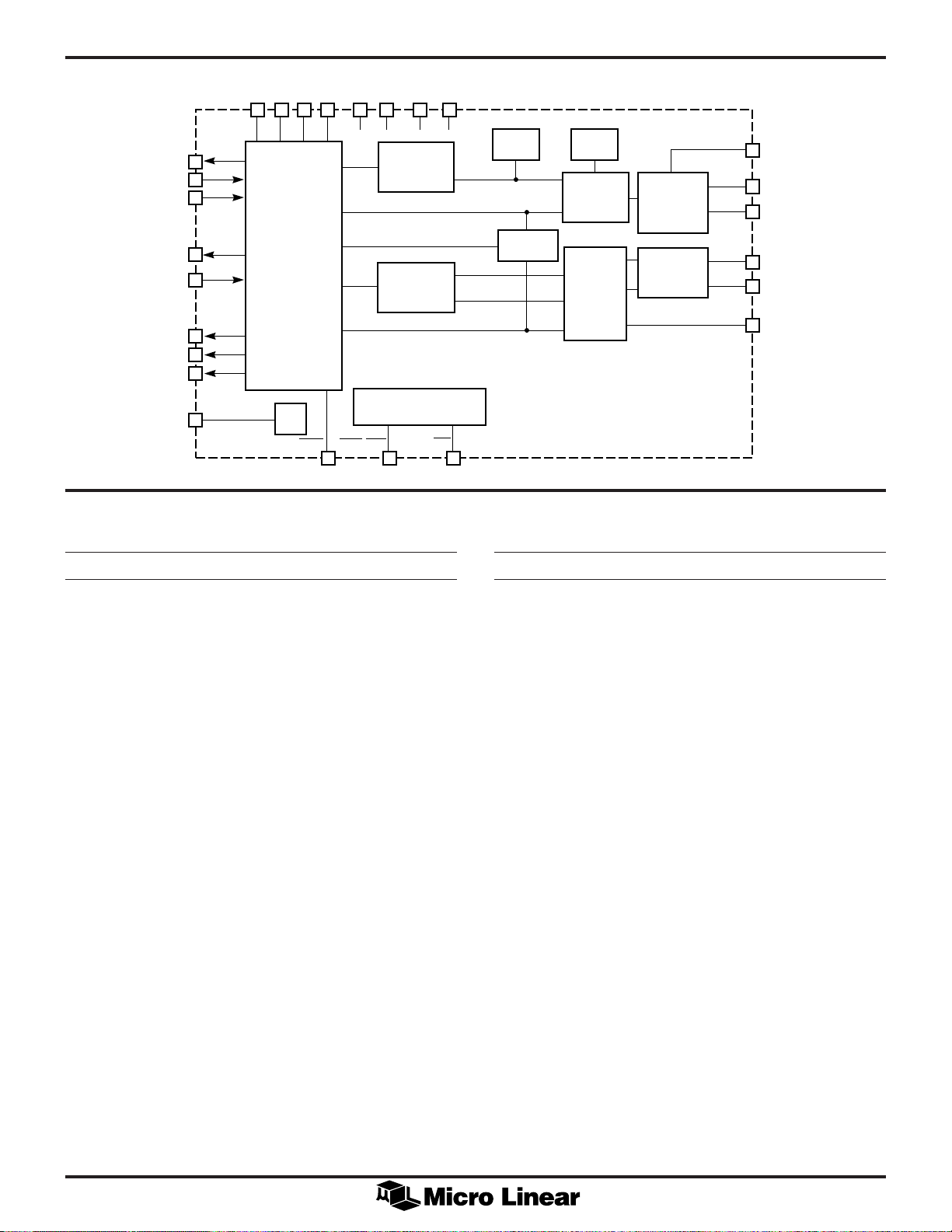
ML2653 BLOCK DIAGRAM
ML2652/ML2653
TxC
TxE
TxD
COL
LPBK
RxC
RxE
RxD
CLK
PIN DESCRIPTION
NAME FUNCTION
CS0 CS1 CS2 FD V
CONTROLLER
INTERFACE
OSC
V
CC
MANCHESTER
DATA
ENABLE
COLLISION
DATA
MANCHESTER
ENABLE
XMT/RCVRPOL LTP
GND
CC
ENCODER
DECODER
LEDS
GND
JABBER
DETECT
COLLISION
DETECT
NAME FUNCTION
LINK
PULSE
XMT
WAVEFORM
GEN & LPF
RECEIVER
CURRENT
DRIVEN XMT
OUTPUT
DRIVER
RECEIVE
LPF
RTX
Tx+
Tx–
Rx+
Rx–
RSL
V
Positive supply. +5V
CC
GND Ground. 0 volts. All inputs and outputs referenced
to this point.
CLK Clock input. There must be either a 20 MHz
crystal or a 20 MHz clock between this pin
and GND.
Tx+ Transmit positive twisted pair output. This output
is a current source that drives the twisted pair
cable through a pulse transformer.
Tx– Transmit negative twisted pair output. This output
is a current source that drives the twisted pair
cable through a pulse transformer.
Rx+ Receive positive twisted pair input. This input
receives data from the twisted pair cable through
a pulse transformer.
Rx– Receive negative twisted pair input. This input
receives data from the twisted pair cable through
a pulse transformer.
DO+ AUI positive transmit output. AUI transmit data
output to optional external transceiver.
DI– AUI negative receive data input from optional
external transceiver.
CI+ AUI positive collision input from optional external
transceiver.
CI– AUI negative collision input from optional
external transceiver.
RTX Transmit current set. An external resistor between
this pin and GND programs the absolute value of
output current on Tx±.
TxC Transmit clock output. Digital output which clocks
the transmit data (TxD) into the device from the
controller.
TxD Transmit data input. Digital input which contains
transmit data from the controller.
TxE Transmit enable input. Digital input from the
controller that indicates when the transmit data
(TxD) is valid.
COL Collision output Digital output to the controller
which indicates when a collision condition is
present.
DO– AUI negative transmit output. AUI transmit data
output to optional external transceiver.
DI+ AUI positive receive data input from optional
external transceiver.
RxC Receive clock output. Digital output which clocks
receive data (RxD) from the device into the
controller.
3
Page 4

ML2652/ML2653
PIN DESCRIPTION
NAME FUNCTION
RxD Receive data output. Digital output which
contains receive data sent to the controller.
RxE Receive data valid. Digital output to the controller
that indicates when the receive data (RxD) is
valid.
LPBK Local loopback. Digital input from the controller
which forces the device to loopback transmit data
without sending it on the media.
FD Full Duplex Enable. When enabled the 10BASE-T
MAU loopback and collision detect are disabled.
LPBK must be disabled when using this function.
CS0 Controller selection input. Digital input which
selects one of four standard controller timing
interfaces. This pin has an internal pulldown
resistor to GND.
CS1 Controller select input. Digital input which selects
one of four standard controller timing interfaces.
This pin has an internal pulldown resistor to GND.
CS2 Controller select input. Digital input which selects
one of four standard controller timing interfaces.
This pin has an internal pulldown resistor to GND.
RSL Receive squelch level select input. Pin has
internal pullup resistor to VCC.
RSL = High Receive squelch level = 10Base-T
RSL = Low Receive squelch level = extended
XMT Transmit status output. Digital output which
indicates data transmission on Tx+ and Tx–.
Pin is open drain output with resistor pullup and is
capable of driving an LED. XMT pin and RCV pin
are the same pin for the ML2653.
(Continued)
distance
NAME FUNCTION
CLS Collision status output. Digital output which
indicates that collision condition has been
detected. Pin is an open drain output with resistor
pullup and is capable of driving an LED.
LTP Link test pass output/input. This pin consists of an
open drain output transistor with a resistor pullup
that serves both as a link test pass output and a
link test disable input. When used as an output,
this pin is capable of driving an LED.
LTP = High, link test failed
LTP = Low, link test pass
LTP = GND, link test disabled
AUI/TP AUI/twisted pair interface select input.
AUI/TP = High, AUI selected
AUI/TP = Low, TP selected
RPOL This pin must be grounded at all times.
JAB Jabber detect output. Digital output which
indicates that the jabber condition has been
detected. Pin is an open drain output with resister
pullup and is capable of driving a LED.
JAB = High, normal
JAB = Low, jabber detected
AUISEL AUI/TP port output status
AUISEL = High, TP port selected
AUISEL = Low, AUI port selected
JABDIS Jabber disable input
JABDIS = High, jabber disabled
JABDIS = Low, normal operation
NC No connect. Leave this pin open circuit.
RCV Receive status output. Digital output which
indicates unsquelched data reception on Rx+
and Rx–. Pin is an open drain output with resistor
pullup and is capable of driving an LED.
ABSOLUTE MAXIMUM RATINGS
Absolute maximum ratings are limits beyond which the
life of the integrated circuit may be impaired. All voltages
unless otherwise specified are measured with respect to
GND. (Note 1)
VCC supply voltage .................................................. +6.5V
All inputs and outputs....................... –0.3V to VCC + 0.3V
Input current per pin.............................................±25 mA
Power dissipation .............................................. 0.75 Watt
4
Storage temperature range ........................ –65°C to 150°C
Junction Temperature .............................................. 150°C
Lead temperature (soldering, 10 sec)....................... 260°C
Thermal Resistance (qJA)
28-Lead PLCC................................................... 60°C/W
44-Lead PLCC................................................... 54°C/W
44-Lead TQFP ................................................... 67°C/W
Page 5

ML2652/ML2653
ELECTRICAL CHARACTERISTICS
(Continued)
Unless otherwise specified TA = 0°C to 70°C, VCC = 5V +5%. Note 2 & 3.
SYMBOL PARAMETER CONDITIONS MIN TYP MAX UNITS
VIL Digital input low voltage All except CLK .8 V
CLK 1.5 V
VIH Digital input high voltage All except CLK 2.0 V
CLK 3.5 V
IIL Digital input low current VIN=GND TxD, TxE, AUI/TP –5 µA
VIN=GND LPBK, CS2–0, LBDIS,JABDIS –5 µA
VIN=GND RSL –10 –25 –50 µA
VIN=GND LTP, RPOL, –15 –250 –500 µA
VIN=GND CLK –300 µA
IIH Digital input high current VIN=VCC TxD, TxE, AUI/TP 1µA
VIN=VCC LPBK, CS2–0, LBDIS, JABDIS 10 25 50 µA
VIN=VCC RSL 1 µA
VIN=VCC LTP, RPOL 1 µA
VIN=VCC CLK 250 µA
CIN Digital input capacitance All except CLK 5 pF
CLK 10 pF
VOL Digital output low voltage IOL=–2mA TxC, COL,
RxC, RxD, RxE .4 V
IOL=–10mA XMT, RCV,
CLS, LTP, RPOL, JAB .6 V
VOH Digital output high voltage IOH=2mA TxC, COL,
RxC, RxD, RxE 4.0 V
IOL=10uA XMT, RCV, CLS,
LTP, RPOL, JAB 2.4 V
ICC VCC supply current TX transmission 140 mA
No transmission 105 mA
Powerdown mode 2 mA
TOV Tx± differential
output voltage RTX = 10K 2.2 2.5 2.8 Vp
THD Tx± harmonic distortion TxD=all ones –27 dB
TCM Tx± common mode
output voltage ± 50 mVp
TCMR Tx± common mode rejection VCM=15vp, 10.1 MHz sine ± 100 mVp
TOVI Tx± differential output
voltage during idle ± 50 mVp
TOIA Tx± output current accuracy RTX=10K 50 mA
TRO Tx± output resistance 1 Mohm
TCO Tx± output capacitance 10 pF
5
Page 6

ML2652/ML2653
ELECTRICAL CHARACTERISTICS
SYMBOL PARAMETER CONDITIONS MIN TYP MAX UNITS
RRI Receive input resistance 2.5K 10K ohms
RCI Receive input capacitance 10 pF
RSON Receive squelch on level RSL=1 275 520 mVp
(Differential zero RSL=0 150 325 mVp
to peak voltage)
RSOF Receive squelch off level RSL=1 150 325 mVp
(Differental zero RSL=0 100 225 mVp
to peak voltage)
DOV DO± differential
output voltage ± 550 ± 1170 mV
DOVI DO± differential
output voltage during idle ± 40 mV
DOUS DO±differential output
voltage return to 0 undershoot –100 mV
(Continued)
DOCMA DO± common mode AC
output voltage ± 40 mV
DOCMA DO± common mode DC
output voltage VCC *.5 V
DIRI DI/CI input resistance 2.5K 10K ohms
DICI DI/CI input capacitance 10 pF
DIBV DI/CI input bias voltage DI/CI floating VCC *.5 V
DISON DI/CI squelch on level –175 –325 mVp
t1 TxC on time 45 55 ns
t2 TxC off time 45 55 ns
t3 TxC period 100 ns
t4 TxE setup time 25 ns
t5 TxE hold time 0 ns
t6 TxD setup time 25 ns
t7 TxD hold time 0 ns
t8 Transmit propagation delay Tx± 60 200 ns
DO± 200 ns
6
Page 7

ML2652/ML2653
ELECTRICAL CHARACTERISTICS
SYMBOL PARAMETER CONDITIONS MIN TYP MAX UNITS
t9 Start of Idle Tx±
Pulse Width DO± 200 350 ns
t10 SOI pulse width to within Tx± 4500 ns
40mV of final value DO± 8000 ns
t11 Transmit output jitter Tx± ± 8.0 ns
t12 Transmit output
rise and fall time Tx± , 10–90% 5 ns
t13 TxE to XMT assert 250 ms
t14 XMT blinker pulse period 95 115 ms
t15 XMT duty cycle 45 55 %
t20 Start of receive packet Rx± 600 ns
to RxE assert DI± 200 ns
(Continued)
DO± ± .5 ns
t21 Start of receive packet Rx+ 1600 ns
to RxC active DI+ 1300 ns
t22 RxC on time 45 900 ns
t23 RxC off time 45 55 ns
t24 RxD valid before RxC 45 ns
t25 RxD valid after RxC 35 ns
t26 RxE assert to RCV assert 250 ms
t27 RCV blinker pulse period 95 115 ms
t28 RCV duty cycle 45 55 %
t29 Receive input jitter Preamble ± 12 ns
Data ± 18 ns
t30 Receive propagation delay Tx± 160 ns
DI± 160 ns
t31 RxC to RxE assert 30 60 ns
t32 RxC to RxE deassert 20 45 ns
t33 RxE deassert to RxC switchover 100 200 ns
7
Page 8

ML2652/ML2653
ELECTRICAL CHARACTERISTICS
SYMBOL PARAMETER CONDITIONS MIN TYP MAX UNITS
t34 Minimum SOI pulse width Tx± 180 ns
required for receive detection DI± 180 ns
t40 Jabber activation delay- 20 150 ms
TxE assert to Tx± disable
t41 Tx± disable to JAB assert 200 ms
t42 Jabber reset time – TxE 250 750 ms
deassert to JAB deassert
t43 Tx± disable to COL assert 50 ns
t44 Tx± disable to CLS assert 50 ns
t45 JAB deassert to COL deassert 50 ns
t46 JAB deassert to CLS deassert 50 ns
(Continued)
t51 Transmit link pulse period 8 24 ms
t52 Minimum link pulse period 2 7 ms
required for receive detection
t52 Maximum link pulse period 25 150 ms
required for receive detection
t53 Receive link pulse no detect 50 150 ms
to LTP deassert
t54 Receive link pulse detect to 2 Link Pulse
LTP assert
t55 AUI/TP to AUISEL delay 200 ns
t60 TxE deassert to COL assert .9 1.0 1.1 µs
t61 COL pulse Width .9 1.0 1.1 µs
t70 Start of RCV packet during Rx± 500 ns
transmission to COL assert
t71 Start of RCV packet during Rx± 500 ns
transmission to CLS assert
t72 End of RCV packet during Rx± 300 ns
transmission to COL deassert
t73 CLS blinker pulse period 95 115 ms
t74 CLS duty cycle 45 55 %
8
Page 9

ML2652/ML2653
ELECTRICAL CHARACTERISTICS
SYMBOL PARAMETER CONDITIONS MIN TYP MAX UNITS
t75 Transmission start during Tx± 300 ns
reception to COL assert
t76 Transmission start during Tx± 250 ns
reception to CLS assert
t77 CI± period 80 120 ns
t78 CI± duty cycle 40 60 %
t79 First valid negative CI± 100 ns
data transition to COL assert
t80 First valid negative CI± 100 ns
data transition to CLS assert
t81 Last CI± positive data 160 250 ns
transition to COL deassert
(Continued)
t82 External clock input jitter 50 ps
Note 1: Absolute maximum ratings are limits beyond which the life of the integrated circuit may be impaired. All voltages unless otherwise specified are measured with
Note 2: Limits are guaranteed by 100% testing, sampling, or correlation with worst-case test conditions.
Note 3: Low Duty cycle pulse testing is performed at T
respect to ground.
.
A
9
Page 10

ML2652/ML2653
TIMING DIAGRAMS
TxC
TxE
TxD
(NRZ)
COL
1
MANCH.
DATA
XMT
TWISTED
PAIR
(Continued)
111100001011
1 1 1100 001 01 0
1 11 100001010
LINK
PULSE
SOI
PULSE
SQE TEST
LINK
PULSE
LINK
PULSE
RCV
TWISTED
PAIR
RxC
RxE
RxD
(NRZ)
Figure 1. Transmit System Timing
10111100001010
1 1110000101 0
10
Figure 2. Receive Timing
Page 11

ML2652/ML2653
TIMING DIAGRAMS
TxC
TxE
TxD
Tx±
XMT
(Continued)
t
4
t
t
6
B0 B1 B2 B3
t
8
t
13
t
1
7
B0 B0 B1 B1 B2 B2 B3 B3
t
11
t
14
t
2
t
5
t
15
Figure 3. Transmit Timing
t
3
t
9
t
12
t
10
40mV
10 10 10 101 0
Rx±
t
20
RxE
(1)
RxC
t
31
(2)
RxC
Tx Tx Tx Tx
RxD
t
26
RCV
NOTE:
1. RxC IS NOT CONTINUOUS DURING IDLE
2. RxC IS CONTINUOUS DURING IDLE
Figure 4. Receive Timing – Start of Frame
t
29
t
t
21
t
22
t
28
22
t
Rx Rx Rx Rx Rx
Rx
t
27
23
t
23
Rx Rx Rx Rx
t
24
1010
t
25
11
Page 12

ML2652/ML2653
TIMING DIAGRAMS
0 0 1 SOI
Rx±
RxE
(1)
RxC
RxC
RxD
Rx Rx Rx Rx Rx
(2)
Rx Rx Rx Rx Rx Tx Tx Tx Tx
t
30
NOTE:
1. RxC IS NOT CONTINUOUS DURING IDLE — 8 EXTRA CLOCKS ADDED FOR CS2 – 0 = 000
2. RxC IS CONTINUOUS DURING IDLE
(Continued)
00 1
Figure 5. Receive Timing – End of Frame
t
34
t
32
5 EXTRA RxC FOR CS2 – 0 = 000
t
33
t
22
TxC
TxE
TxD
Tx±
COL
JAB
CLS
t
40
t
43
t
41
t
44
Figure 6. Jabber Timing (ML2652 only.)
t
42
t
45
t
46
12
Page 13

ML2652/ML2653
TIMING DIAGRAMS
Tx±
Rx±
LTP
AUI/TP
AUISEL
(Continued)
TRANSMIT
RECEIVE
INTERFACE SELECT
t
51
t
52
t
55
t
53
Figure 7. Link Pulse Timing
t
54
t
55
TxC
TxE
TxD
COL
t
60
t
61
Figure 8. SQE Test Timing
13
Page 14

ML2652/ML2653
TIMING DIAGRAMS
TxD
Tx±
RxD
Rx±
COL
CLS
(Continued)
t
70
t
71
DATA MAY BE INVALID
t
73
t
74
t
72
Rx±
TxE
TxD
Tx±
COL
CLS
Figure 9. Collision Timing Reception During Transmission
t
75
t
76
t
74
t
73
t
82
14
Figure 10. Collision Timing Transmission During Reception
Page 15

ML2652/ML2653
TIMING DIAGRAMS
CI±
COL
CLS
(Continued)
t
78
t
79
t
80
Figure 11. CI± Collision
APPLICATION CIRCUIT — ML2652
+5V
V
CCVCC
TxC
TxD
TxE
COL
RxC
RxD
RxE
FD
LPBK
CS0
CS1
CS2
JABDIS
5.1K
RSL
AUI/TP
XMT
RCV
CLS
AUISEL
LTP
RPOL
JAB
CLK GND GND RTX
ML2652
(SEE TABLE 1)
SEEQ 8003
SEEQ 8005
NSC DP8390
AMD AM7990
INTEL 82586
INTEL 82596
ETHERNET
CONTROLLER
+5V
510Ω
510Ω
+5V
5.1K
t
77
0.1µF
0.1µF
Tx+
Tx–
Rx+
Rx–
DO+
DO–
CI+
CI–
DI+
DI–
t
78
t
73
+5V +5V
200Ω
1%
98Ω
1%
78Ω
78Ω
78Ω
200Ω
1%
t
81
+5V
2:1
1:1
AUI
RJ45
6
10K
Figure 12
15
Page 16

ML2652/ML2653
FUNCTIONAL DESCRIPTION
GENERAL
The ML2652 and ML2653 are composed of a transmitter
section, receive section and some miscellaneous
functions.
The transmit section consists of the manchester encoder,
AUI, jabber detect, link pulse generator, start of idle (SOI)
pulse generator, waveform generator, and line driver. The
purpose of the transmit section is to take data from the
controller, encode it, and transmit it over either the AUI or
twisted pair interface. In addition, the transmit section
generates link pulses, start of idle pulses, and checks for
jabber condition. The transmitter keeps the data jitter to a
maximum of ±8.0ns, and the maximum delay through the
transmission section is less than 2 bits, or 200ns.
The receive section consists of the manchester decoder,
collision detect, AUI, receive LPF, receive comparators,
receive squelch, automatic polarity correct, start of idle
(SOI) detect, and link pulse detect. The purpose of the
receive section is to take data from either the twisted pair
cable or AUI, decode it, then send the data to the
APPLICATION CIRCUIT — ML2653
controller via the controller interface. In addition, the
receive section detects and automatically corrects for
reverse polarity, detects link pulses, detects start of idle
pulses, and implements an intelligent receive squelch
algorithm. The receive section can successfully lock onto
an incoming data that contains ±18ns of jitter in less than
1.6µs.
The miscellaneous functions are the controller interface,
single pin crystal oscillator, AUI, loopback modes, test
mode, and powerdown mode. The ML2653 has no AUI
interface output.
The following text describes each of these blocks and
functions in more detail. Refer to the block diagram.
TRANSMISSION
The transmit data (NRZ) is first clocked into the device
through the controller interface. The device can be
digitally programmed to accommodate any one of four
standard Ethernet controllers as described in Controller
section.
(SEE TABLE 1)
SEEQ 8003
SEEQ 8005
NSC DP8390
AMD AM7990
INTEL 82586
INTEL 82596
ETHERNET
CONTROLLER
+5V
510Ω
510Ω
+5V
+5V
V
CCVCC
TxC
TxD
TxE
COL
RxC
RxD
RxE
FD
LPBK
CS0
CS1
CS2
RSL
5.1K
XMT/RCV
LTP
RPOL
CLK GND GND RTX
0.1µF
0.1µF
ML2653
10K
Tx+
Tx–
Rx+
Rx–
+5V +5V
200Ω
1%
98Ω
1%
200Ω
1%
+5V
2:1
1:1
RJ45
16
Figure 13
Page 17

ML2652/ML2653
FUNCTIONAL DESCRIPTION
Then the NRZ data is encoded by the manchester encoder
as shown in transmit timing diagram in Figure 1.
The manchester encoded data then goes to either the AUI
or twisted pair interface. The selection of the appropriate
interface is automatic. If the AUI is selected, the
manchester encoded data is transmitted out differentially
on the DO+ and DO– pins, and the twisted pair line driver
is disabled. If the twisted pair interface is selected, the
manchester encoded data is transmitted out differentially
on Tx+ and Tx– pins, and the transmit AUI is disabled.
Refer to the AUI section for details on how the AUI and
automatic interface selection is accomplished.
Assuming that the twisted pair interface is selected, the
Manchester encoded data then goes to the transmit
waveform generator. The transmit waveform generator
takes the digital Manchester encoded data and generates a
waveform. When this waveform is passed through the
cable model in the 10BASE-T standard (figure 14–7 IEEE
Std 802.3i–1990) it meets the voltage template (figure 14–
9 IEEE Std 802.3i–1990).
The transmit waveform generator is composed of a 16 x 4
bit ROM, 4 bit DAC, 3rd order LPF, and clock generator.
The DAC is used to synthesize a stair-step representation of
a signal that will meet the required output template. The
ROM stores the digital representation of the output signal
and provides a digital input to the DAC. The ROM is
addressed by a 16 phase clock generator that is locked to
the transmit clock TxC. The high frequency content present
in the output of the DAC is removed by a 3rd order
continuous LPF which smooths the output.
The transmit line driver takes the output of the waveform
generator and converts this voltage to a differential output
current on Tx+ and Tx– pins. When one transmit output
(either Tx+ or Tx–) is sinking current, the other output is
high impedance, and vice versa. In this way, a differential
output voltage is developed by sinking this output current
through two external 200 ohm terminating resistor and a
2:1 transformer as shown in Figure 12.
(Continued)
RTX = K*Vb/Iout
= 125*4v/50mA
RTX = 10kW
When data is being transmitted (and there is no collision
or link pulse fail condition), the transmit data is looped
back to the receive path, and the Manchester decoder will
lock onto the transmit data stream.
After data transmission is completed, the transmitter sends
a start of idle (SOI) pulse to signal the end of a packet.
During the idle period, Tx+ and Tx– are held low.
Occasionally, link pulses are transmitted during the idle
period.
The XMT pin is an output that indicates transmit activity.
The pin consists of an open drain output with an internal
pull-up resistor and can drive an LED from VCC or another
digital input. In order to make an LED visible, XMT has an
internal blinker circuit that generates a 100ms blink (50ms
high, 50ms low) that is triggered when a trans-mission
starts. At the completion of the 100ms blink period, if a
transmission is in progress, another 100ms blink is
generated.
RECEPTION
The twisted pair receive data is typically transformer
coupled and terminated with an external resistor as shown
in Figure 12.
The output of the transformer is then applied to the device
input pins Rx+ and Rx–. The input is differential, and the
common mode input voltage is biased to VCC/2 by two
internal 10K bias resistors from Rx+, Rx– to VCC/2.
The Rx+ and Rx– inputs then go to the receive filter. The
receive filter is a continuous 3rd order LPF and has the
following characteristics:
1. 3 dB cut-off frequency 15 MHz
Setting the external terminating resistors to 200 ohms as
shown in Figure 12 will implement a 100 ohm terminating
impedance when looking back through the transformer. If
other terminating impedances are required (such as 150
ohm), the terminating resistor values can be adjusted
accordingly as long as the output current stays within the
minimum and maximum limits (30–70mA).
The absolute value of the output current, and subsequently
the output voltage level, is set by an external resistor
between RTX and GND. If RTX = 10k ohms and Tx± is
terminated as shown in Figure 12, the output level is
±2.5V which meets 802.3i–1990 differential output
voltage requirements. If a different output current/voltage
level is desired, the level can be changed by changing the
value of RTX according to the following formula:
2. Insertion Loss (5–10 MHz) - 1.0 dB
3. 30 MHz attenuation 17.5 dB min.
The output of the filter goes to the receive comparators.
There are two receive comparators inside the chip,
threshold and zero crossing. The threshold comparator
determines if the receive data is valid by checking the
input signal level against a predetermined positive and
negative squelch level. Once the threshold comparator
determines that valid data is being received, the zero
crossing comparator senses zero crossings to determine
data transitions. Both comparators are fast enough to
respond to 12ns pulse widths with minimum squelch
overdrive.
17
Page 18

ML2652/ML2653
FUNCTIONAL DESCRIPTION
The receive squelch circuit determines when data on
incoming Rx+, Rx– is valid. The receive squelch is
considered “on” when the data is deemed to be invalid,
and the receive squelch is considered “off” when data is
determined to be valid.
The input signal must meet the following criteria in order
to turn receive squelch off and be recognized as valid
data:
1. The input signal must exceed the receive squelch
on level. When this occurs, a 400ns squelch interval
timer is started.
2. During the 400ns squelch interval, the input signal
must go from one squelch threshold to the opposite
polarity squelch threshold in less than 127ns.
3. During the 400ns squelch interval, the input signal
has to make less than 9 squelch threshold to opposite
polarity squelch threshold crossings.
When the receive squelch is turned off, the receive
squelch off level is reduced to 2/3 of receive squelch on
level.
The receive squelch will be turned back on if either the
incoming data peaks go below the receive squelch off
level for 400ns or the start of idle (SOI) pulse is detected.
The receive squelch on level can be digitally programmed
for one of two possible levels by using the RSL pin. When
RSL = 1, the squelch on level complies with the IEEE
802.3i–1990 specification. When RSL = 0, the receive
squelch on level is lowered in order to accommodate
greater receive attenuation and consequently longer
twisted pair cable lengths. The receive squelch on level
can be programmed as follows:
(Continued)
RECEIVE SQUELCH ON LEVEL
RSL Application Min Typ Max
1 10BASE-T 300 585mV
0 Long Distance 200 390mV
The RCV pin is an output that indicates receive activity.
The pin consists of an open drain output with an internal
pull-up resistor and can drive an LED from VCC or another
digital input. In order to make an LED visible, RCV has an
internal blinker circuit that generates a 100ms blink (50ms
high, 50ms low) that is triggered when reception starts. At
the completion of the 100ms blink period, if reception is
in progress, another 100ms blink is generated.
The manchester decoder receives data from either the
twisted pair interface (as described above) or the AUI
(described in AUI section).
The manchester decoder is responsible for recovering
clock and data from the incoming receive bit stream.
Clock and data recovery is accomplished by a digital PLL
which can lock on the incoming bit stream in less than
1.6µs.
The clock (RxC) and NRZ data (RxD) are then output to
the external world via the controller interface.
SOI
A start of idle (SOI) pulse is sent at the end of transmission in
order to signal to all receivers that transmission has ended
and the idle period begins. Thus, the transmit section has an
SOI generator and the receive section has an SOI detector.
The transmit SOI pulse generator inserts an SOI pulse at the
end of each transmission. The SOI pulse is typically a 250ns
positive pulse inserted after the last positive data transition.
Depending on the data pattern, the positive data transition
could occur either in the middle or at the end of the last bit
cell. So the actual width of the transmitted SOI pulse can
vary from 250–300ns, typically.
The receive SOI detector senses the SOI pulse using the zero
crossing comparator. When the SOI pulse is detected, the
receiver signals to the controller that receive data is no
longer valid and turns the receive squelch on.
LINK PULSE
During the idle period, link pulses are sent by the transmitter
and detected by the receiver so that the integrity of the
twisted pair link can be continuously monitored. Thus, the
transmit section has a link pulse generator, and the receiver
has a link pulse detector.
The transmit link pulse generator transmits a 100ns wide
positive pulse (Tx+ high, Tx– low) every 16 ±8ms.
IEEE 802.3i–1990 Section 14 requires the link pulse to be
shaped to meet a template when passed or not passed
through the twisted pair line model. The transmit waveform
generator takes the link pulse and generates the waveform
on TX± when passed or not passed through the twisted pair
line model.
The receiver monitors the receive input to determine if the
link pulses are present. When the device is in the link pulse
pass state, normal packet transmission and reception can
occur. All link pulses less than 2–7ms apart are ignored
while in the link pass state. If no link pulses or receive
packets are detected for a period of 50–150ms, the device
goes into the link pulse fail state.
When the device is in the link pulse fail state, reception is
inhibited and the transmitter is placed in the idle state (no
data transmission but link pulses are still transmitted). In
order for the device to exit the link pulse fail state, one
complete packet or 4 consecutive link pulses must be
detected, and transmit and receive must be idle.
Consecutive link pulses are defined as pulses that occur
within 25–150ms of each other. If the link pulses occur
18
Page 19

ML2652/ML2653
FUNCTIONAL DESCRIPTION
2–7ms apart in the link fail state, the device ignores the link
pulses and resets the number of consecutive link pulses to
zero. After the link pulse fail state is exited, transmission and
reception can be resumed.
Link pulse status is indicated by the LTP pin. LTP is a dual
function input/output pin that acts both as an active low link
test pass output and a link test disable input. The pin consists
of an open drain output with an internal pull-up resistor. If
the pin is tied to GND, the pin acts as an input and the link
test function is disabled. If the pin is not tied to GND, the pin
acts as an active low link test pass output and can drive an
LED from VCC or another digital output. Thus, the LED is lit
when the link test is passing.
(Continued)
JABBER
The transmit section contains a jabber detect circuit.
Jabber is a fault condition characterized by a babbling
transmitter. The ML2652 and ML2653 detect jabber when
a transmission packet exceeds 20–150ms in length. If
jabber detect occurs, the transmit output is disabled, the
collision signal COL is sent over the controller interface,
and the JAB pin is pulled low. The device remains in the
jabber detect state until there is at least 250–750ms of
continuous non-transmission. Note that link pulses
continue to be transmitted even when the device is in the
jabber condition.
The jabber detection circuitry can be disabled (only on the
ML2652) with the JABDIS pin for testing and diagnostic
purposes. Disabling jabber means that a jabber condition
is never recognized, even when it occurs. JABDIS is an
active high jabber disable input and has an internal pulldown resistor to GND.
COLLISION
Collision occurs whenever the DTE card is transmitting
and receiving data simultaneously. However, the collision
circuit on the ML2652 operates differently depending on
whether twisted pair interface or AUI is being used.
When the twisted pair interface is used, collision occurs
whenever the device is transmitting and receiving data
simultaneously, that is when both RxE and TxE are active.
The collision state is indicated by COL and CLS pins. COL
is used to signal collision to the controller. CLS is an active
low open drain output. CLS is activated during Jabber, but
not during SQE test while COL is activated during both.
When the AUI is used (ML2652 only), collision is no
longer detected from simultaneous transmission and
reception, but the collision state is determined when a
collision signal is present on the AUI collision inputs, CI+
and CI–. A 10 MHz square wave has to be applied to this
input in order for the device to signal the collision state on
COL and CLS.
The CLS pin is an output that indicates collision activity.
The pin consists of an open drain output with an internal
pull-up resistor and can drive an LED from VCC or another
digital input. In order to make an LED visible, CLS has an
internal blinker circuit that generates a 100ms blink (50ms
high, 50ms low) that is triggered when a collision starts. At
the completion of the 100ms blink period, if collision is in
progress, another 100ms blink is generated.
SQE TEST
When the twisted pair interface is used, the device tests
the collision circuitry at the end of each transmission by
sending a 1µs collision pulse over the COL pin. This is
known as SQE (signal quality error) test and is shown in
the transmit timing diagram in Figure 1. The SQE test is
disabled if the device is in jabber detect state or link pulse
fail condition.
When AUI is used (ML2652), the SQE test pulse is
generated by an external MAU and the external MAU
sends the SQE test pulse to the ML2652 via the collision
inputs , CI+ and CI–. The ML2652 then relays the collision
signal to the controller via the COL and CLS output pins.
RECEIVE POLARITY DETECT AND AUTO CORRECTION
The ML2652 and ML2653 contain an auto-polarity circuit
that detects the polarity of the receive twisted pair leads,
Rx+ and RX-and internally reverses the leads if their
polarity is incorrect.
When the device is powered up, it is assumed that the
polarity is correct and no polarity correction occurs. Then
receive polarity is continuously monitored by checking the
polarity of the SOI and link pulses since they are always
positive pulses. If either 2 consecutive SOI or 4
consecutive link pulses have incorrect RX± polarity, then
the auto-polarity circuit internally reverses the Rx+ and
Rx– connections.
AUI (APPLIES ONLY TO ML2652)
The ML2652 can be used with an external MAU via the
Attachment Unit Interface (AUI). When the AUI is used,
the internal MAU functions and twisted pair interface are
disabled, and the device only uses the manchester
encoder and decoder functions, as shown in the block
diagram. The AUI consists of three differential signal pairs:
DI, DO, and CI. The function of each pair is described
below.
The DO+ and DO– are differential outputs to the external
MAU which contain the transmit data output from the
Manchester encoder. The DO+ and DO– output drivers
are capable of driving 50 meters of 78 ohm cable with less
than 5ns rise and fall time and less than ±0.5ns of jitter. In
addition, at the end of transmission, the AUI output driver
inserts a 200ns minimum pulse and meets the turnoff and
idle characteristics specified in IEEE 802.3–1988. An
external 78 ohm resistor across DO+ and DO– is required
as shown in Figure 12 to develop the proper output levels
from the internal current sources. The DO+ and DO–
19
Page 20

ML2652/ML2653
FUNCTIONAL DESCRIPTION
outputs can be coupled to an external MAU with either
capacitors or a transformer. The ML2652 meets all AUI
transmitter specifications outlined in IEEE 802.3–1988
Section 7.
DI+ and DI– are inputs from the external MAU which
contain the receive data that goes to the manchester
decoder.
The DI+ and DI– inputs contain an AUI DI squelch circuit
which determines when incoming data on DI+ and DI– is
valid. The DI squelch is considered “on” when the data is
deemed to be invalid, and the DI squelch is considered
“off” when data is determined to be valid.
The input signal on DI+ and DI– must meet the following
criteria in order to turn receive squelch off and be
recognized as valid data:
1. The input signal must exceed the negative AUI DI
squelch on level.
2. The input signal must exceed the negative AUI DI
squelch on level for more than 20ns.
(Continued)
The AUISEL pin is a digital status output that indicates
which interface has been selected for data transfer, either
twisted pair or AUI. The pin consists of an open drain
output with an internal pull-up resistor and can drive an
LED from VCC or another digital input. AUISEL = High
indicates that the twisted pair interface has been selected.
AUISEL = Low indicates that the AUI interface has been
selected.
The ML2652 has the capability to automatically select
between the twisted pair interface and AUI. This automatic
interface selection is accomplished by tying the LTP
output pin to the AUI/TP input pin. When these two pins
are connected together, if valid link pulses are detected, it
is assumed that the twisted pair interface is being used.
This causes LTP output to go low, thus forcing AUI/TP low,
and thus enabling the twisted pair interface. If no valid
link pulses are detected, it is assumed that the twisted pair
interface is not being used, thus causing LTP to go high,
thus forcing AUI/TP high, thus enabling the AUI interface.
If valid link pulses reappear, the device will automatically
disable the AUI and enable the twisted pair interface. The
algorithm for determining valid link pulses is described in
the Link Pulse section.
When the DI squelch is turned off, the DI squelch off level
is reduced to 2/3 of the DI squelch on level.
The DI squelch circuit will be turned back on if the idle
period is detected by no DI squelch level transitions for
more than 180ns.
An external 78 ohm termination resistor is needed across
DI+ and DI– as shown in Figure 12. The DI+ and DI–
inputs can be coupled from an external MAU into the
ML2652 with either capacitors or a transformer. The
ML2652 meets all AUI receiver specifications outlined in
IEEE 802.3–1988 Section 7.
CI+ and CI– are inputs from the external MAU which
contain the 10 MHz ± 15% collision signal as defined in
IEEE 802.3–1988 Section 7. The CI+ and CI– inputs
contain the same squelch circuit used on the DI inputs
described in previous paragraphs in this section.
An external 78 ohm termination resistor is needed across
CI+ and CI– as shown in Figure 12. The CI+ and CI– inputs
can be coupled from an external MAU into the ML2652
with either capacitors (shown in Figure 12) or a
transformer. The ML2652 meets all AUI receiver
specifications outlined in IEEE 802.3–1988 Section 7.
LOOPBACK
LPBK provides a loopback through the manchester
encoder/decoder, but not through the on-chip 10BASE-T
MAU. No data will go out on either the AUI port or the
twisted pair port in this mode. This same function is found
on many discrete manchester encoder/decoders.
IEEE 802.3 MAUs normally loop the transmit data (DO+)
when transmitting with no collisions. When using an
external transceiver through the ML2652's AUI port, the
controller can first check the local loopback by setting
LPBK. If it passes this test it can then check the AUI cable
and external MAU by doing the normal MAU loopback.
FULL DUPLEX OPERATION
The ML2652 and ML2653 are capable of operating in the
full duplex mode which transmits and receives data
simultaneously. In the full duplex mode the collision
circuitry is disabled just as it is in the loopback mode. To
achieve full duplex operation the full duplex pin FD is
enabled and the loopback pin LPBK must be disabled.
Both of these conditions must be present to operate in the
full duplex mode.
The ML2652 contains an AUI/TP select input pin which
controls whether the AUI or twisted pair interface is to be
used for data transmission and reception. When AUI/
Twisted Pair Switching = High, the AUI is used for data
transmission and reception. When AUI/Twisted Pair
Switching = Low, the twisted pair interface is used for data
transmission and reception.
20
CONTROLLER INTERFACE
The ML2652 and ML2653 has a flexible and
programmable digital interface which enables it to directly
interface to Ethernet controllers manufactured by Intel,
AMD, National and Seeq.
Page 21

ML2652/ML2653
FUNCTIONAL DESCRIPTION
(Continued)
The controller interface consists of seven pins. TxC, TxD,
and TxE are the transmit clock output, transmit data input,
and transmit data enable input, respectively. RxC, RxD,
and RxE are the receive clock output, receive data output,
and receive data enable output, respectively. COL is the
collision detect output.
All the standard Ethernet controllers use a similar
controller interface but differ in the polarity of COL, LPBK,
TxE and RxE, and in what edge of TxC and RxC that clocks
in the data. They also differ on whether the RxC clock
needs to be continuous or not during idle, and on the
polarity of RxD during idle. In order to accommodate the
different controller interface definitions, the controller
select pins, CS2–0, modify these signals according to
Table 1.
POWERDOWN
The device can be placed in the power down mode with
the controller select pins CS2–0 as described in Table 1.
When in powerdown mode, the current consumption is
reduced to less than ZmA and all device functions are
disabled.
CRYSTAL OSCILLATOR
The ML2652 requires an accurate 20 MHz reference for
internal clock generation. This can be achieved by
connecting an external crystal or an external clock
between the CLK and GND pins.
If an external clock is used, it must have a frequency of
20 MHz ±0.01% and have high and low levels of 3.5 and
1.5 volts.
If a crystal is used, the crystal should be placed physically
as close as possible to the CLK and GND pins, especially
CLK. No other external capacitors or components are
required. The crystal should have the following
characteristics:
1. Parallel resonant type
2. Frequency: 20 MHz
3. Tolerance: ±0.005% @ 25°C
4. Less than 0.005% frequency drift across
temperature.
5. Maximum equiv. series resistance:
15 ohms @ 1–200µW
30 ohms @ 0.01–1µW
6. Typical load capacitance: 20pF
7. Maximum case capacitance: 5pF
Table 1. Controller Select Pin Definitions
Idl Idl
CS2–0 TxC TxE RxC RxE COL LPBK RxC RxD Controller
0 0 0 r h r h h h m l NSC DP8390
0 0 1flfll lnhiIntel 82586/96
0 1 0 r h r h h h n hi AMD AM7990
Motorola*
0 1 1 f h r h h l c lo Seeq 8003/5
1 0 0———————— —
1 0 1———————— —
1 1 0———————— —
1 1 1———————— PDN mode
r = rising edge clocks data h = active high c = RxC required continuously
f = falling edge clocks data l = active low n = RxC only during RxD transmission
* AMD mode is also recommended for all Motorola's QUICC, Power QUICC or simlar Communications Controllrs (MPC850, MPC860m ....). These controllers should be 5V or
3.3 V devices with 5V-friendly I/O pins
m = RxC only during RxD transmission + 5 extra RxC cycles
21
Page 22

ML2652/ML2653
PHYSICAL DIMENSIONS
0.685 - 0.695
(17.40 - 17.65)
0.650 - 0.656
(16.51 - 16.66)
1
0.042 - 0.048
(1.07 - 1.22)
12
0.050 BSC
(1.27 BSC)
PIN 1 ID
23
0.026 - 0.032
(0.66 - 0.81)
inches (millimeters)
Package: Q44
44-Pin PLCC
0.650 - 0.656
34
(16.51 - 16.66)
0.165 - 0.180
(4.06 - 4.57)
0.685 - 0.695
(17.40 - 17.65)
0.148 - 0.156
(3.76 - 3.96)
0.042 - 0.056
(1.07 - 1.42)
0.009 - 0.011
(0.23 - 0.28)
0.025 - 0.045
(0.63 - 1.14)
(RADIUS)
0.100 - 0.112
(2.54 - 2.84)
0.500 BSC
(12.70 BSC)
0.590 - 0.630
(14.99 - 16.00)
0.013 - 0.021
0.042 - 0.048
(1.07 - 1.22)
(0.33 - 0.53)
8
0.485 - 0.495
(12.32 - 12.57)
0.450 - 0.456
(11.43 - 11.58)
PIN 1 ID
0.050 BSC
(1.27 BSC)
0.026 - 0.032
(0.66 - 0.81)
SEATING PLANE
1
15
0.450 - 0.456
22
(11.43 - 11.58)
0.165 - 0.180
(4.06 - 4.57)
Package: Q28
28-Pin PLCC
0.485 - 0.495
(12.32 - 12.57)
0.148 - 0.156
(3.76 - 3.96)
0.042 - 0.056
(1.07 - 1.42)
0.009 - 0.011
(0.23 - 0.28)
0.025 - 0.045
(0.63 - 1.14)
(RADIUS)
0.099 - 0.110
(2.51 - 2.79)
0.300 BSC
(7.62 BSC)
0.390 - 0.430
(9.90 - 10.92)
22
0.013 - 0.021
(0.33 - 0.53)
SEATING PLANE
Page 23

ML2652/ML2653
PHYSICAL DIMENSIONS
0.472 BSC
(12.00 BSC)
0.394 BSC
(10.00 BSC)
1
PIN 1 ID
12
0.032 BSC
(0.80 BSC)
inches (millimeters)
Package: H44-10
44-Pin (10 x 10 x 1mm) TQFP
34
0.394 BSC
(10.00 BSC)
23
0.012 - 0.018
(0.29 - 0.45)
0.472 BSC
(12.00 BSC)
0.048 MAX
(1.20 MAX)
0.037 - 0.041
(0.95 - 1.05)
0º - 8º
0.003 - 0.008
(0.09 - 0.20)
0.018 - 0.030
(0.45 - 0.75)
SEATING PLANE
ORDERING INFORMATION
PART NUMBER TEMPERATURE RANGE PACKAGE
ML2652CQ 0°C to 70°C 44-Pin PLCC (Q44)
ML2653CQ 0°C to 70°C 28-Pin PLCC (Q28)
ML2653CH 0°C to 70°C 44-Pin TQFP (H44-10)
© Micro Linear 1998. is a registered trademark of Micro Linear Corporation. All other trademarks are the property of their respective owners.
Products described herein may be covered by one or more of the following U.S. patents: 4,897,611; 4,964,026; 5,027,116; 5,281,862; 5,283,483; 5,418,502;
5,508,570; 5,510,727; 5,523,940; 5,546,017; 5,559,470; 5,565,761; 5,592,128; 5,594,376; 5,652,479; 5,661,427; 5,663,874; 5,672,959; 5,689,167; 5,714,897;
5,717,798; 5,742,151; 5,747,977; 5,754,012; 5,757,174; 5,767,653; 5,777,514; 5,793,168; 5,798,635; 5,804,950; 5,808,455; 5,811,999; 5,818,207; 5,818,669;
5,825,165; 5,825,223; 5,838,723. Japan: 2,598,946; 2,619,299; 2,704,176; 2,821,714. Other patents are pending.
Micro Linear reserves the right to make changes to any product herein to improve reliability, function or design. Micro Linear does not assume any liability
arising out of the application or use of any product described herein, neither does it convey any license under its patent right nor the rights of others. The circuits
contained in this data sheet are offered as possible applications only. Micro Linear makes no warranties or representations as to whether the illustrated circuits
infringe any intellectual property rights of others, and will accept no responsibility or liability for use of any application herein. The customer is urged to consult
with appropriate legal counsel before deciding on a particular application.
DS2652_53-01
2092 Concourse Drive
San Jose, CA 95131
Tel: 408/433-5200
Fax: 408/432-0295
www.microlinear.com
12/9/98 Printed in U.S.A.
23
 Loading...