

Page 1

FEDL2500-01
FEDL2500-01
¡ Semiconductor ML2500
¡ Semiconductor
This version: Jul. 2000
Previous version: Jun. 1999
ML2500
Analog-Storage Single-chip Record/Playback LSI with 1M Bit-Cell Flash Memory
This document contains minimum specifications. For full specifications, please contact your
nearest Oki office or representative.
GENERAL DESCRIPTION
Thanks to newly developed Analog Multi-Level Storage technology, ML2500 stores noncompressed analog source signal directly into on-chip 1M Bit-Cell Flash memory. The result is
superb sound quality without noise and distortions introduced through coding/decoding, and
impressive long-time record/playback capability up to 256 sec. ML2500 is fully controllable by
an external MCU via the industry's standard Serial Peripheral Interface.
In addition, no backup requirement and low operating voltage (2.7 to 3.3 V) make the LSI an ideal
choice for compact, handy and portable terminals. ML2500 is a true shingle-chip solution to
record/playback subsystem for use with today's size-critical electronic products.
FEATURES
• On-chip non-volatile 1M bit-cell Flash memory
Program/Erase Cycles : 10,000 cycles
Data Retention : 10 years
• MCU Interface
Serial Peripheral Interface (SPI; Mode 0)
• Record/Playback Time Length (With the int. Osc. or ext. clock at 8.192 MHz)
ap. 160 sec (At fsam = 6.4 kHz)
ap. 190 sec (At fsam = 5.3 kHz)
ap. 256 sec (At fsam = 4.0 kHz)
• Selectable Sampling Frequencies
4.0 kHz, 5.3 kHz, 6.4 kHz
• Maximum number of recording phrases: 320 phrases
• Phrase Control
Fully controllable with user-definable Start, Stop addresses
• Built-in LPF/Smoothing Filter (LPF attenuation –40dB/oct)
• Built-in Oscillation Circuit (8.192 MHz), No oscillator required
Optional external clock input (Clock Frequency 4.0 MHz to 8.192 MHz)
• Power Supply : 2.7 to 3.3 V
• Operating Temperature:
–10 to +70°C (guaranteed for both function and voice quality)
–40 to +85°C (guaranteed for function only) *Notice
*Notice
The voice quality can deteriorate at temperatures beyond the range of –10 to +70°C.
DC and AC characteristics in this data sheet are specified for –10 to +70°C operating
temperature range.
• Package:
32-pin Plastic TSOP (TSOPI32-P-814-0.50-1K) (Product name: ML2500TA)
1/7
Page 2
FEDL2500-01
¡ Semiconductor ML2500
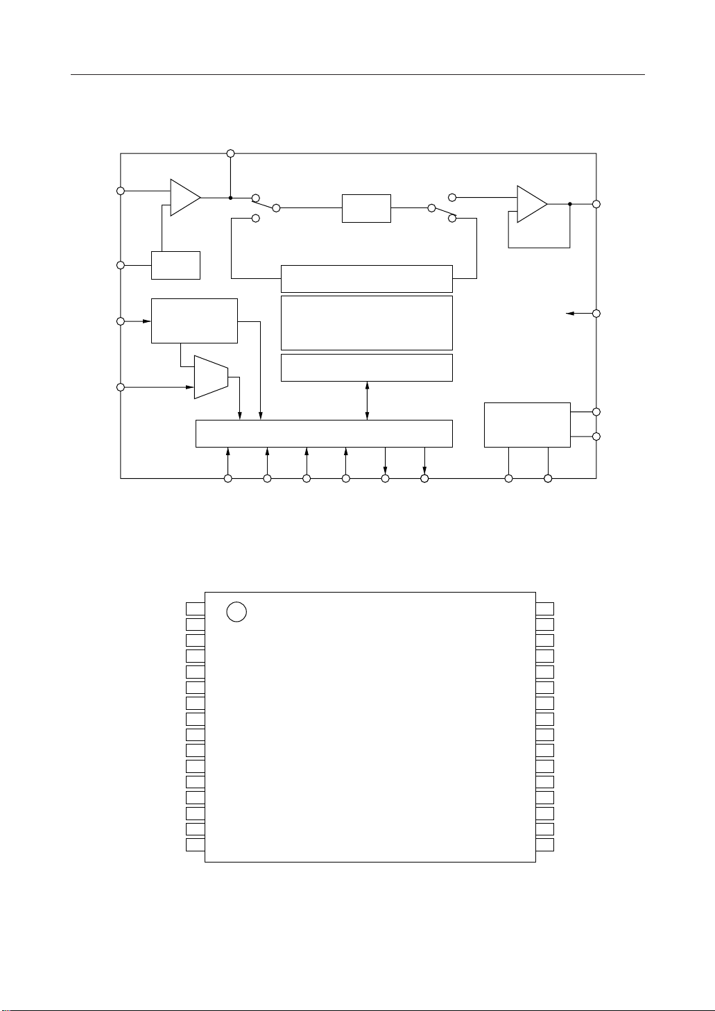
BLOCK DIAGRAM
LOUT
LIN
LPF
AOUT
SG
ROSC
EXTCLK
SG
Internal
Oscillator
MUX
Analog Write & Read Circuits
Serial Peripheral Interface & Controller
RESET
CS SCK DI DO MON DVDDDGND
PIN CONFIGURATION (TOP VIEW)
132
DV
DD
RESET
EXTCLK
TEST2
TEST2
231
330
CS
429
SCK
528
DI
627
DO
726
MON
825
924
NC
10 23
NC
11 22
12 21
NC
13 20
14 19
NC
15 18
ROSC
16 17
DGND
1M Bit Cell
Analog Storage Flash
Memory Array
Address Decoder
Power
Supplies
AV
DD
LIN
LOUT
TEST2
TEST2
AOUT
SG
NC
TEST1
NC
TEST2
NC
TEST2
NC
TEST2
AGND
TEST1
AV
DD
AGND
NC: No connection. Keep NC pins open.
32-Pin Plastic TSOP (Type
11
1)
11
2/7
Page 3
FEDL2500-01
¡ Semiconductor ML2500
PIN DESCRIPTIONS
Pin
5
3
2
15
8
7
26
31
20, 22, 28, 29
24
1
32
Symbol Type Description
DI I Serial input pin for command data.
DO O Serial output pin for status data.6
SCK I Shift clock input pin for the DI and the DO pins.4
CS I
RESET I
ROSC I
EXTCLK I
MON O Output "H" level during recording/playback operation.
SG O
LIN I
LOUT O Output pin from the internal OP amplifier.30
AOUT O Analog waveform output. Connect to an amplifier to drive a SP.27
TEST2 O
TEST1 I LSI's testing pin. Must be connected to DGND.
DV
DD
DGND — Digital Ground pin.16
AV
DD
AGND — Analog Ground pin.17
Chip select pin. "L" level input enables data input/output through the serial
interface.
RESET input pin, resetting the serial interface circuit only. "L" level input to
this pin initializes the serial interface. Must input "L" pulse after each power-on.
Insert a 30 kW resistor (Precision within ±1%) between this pin and the DGND pin.
The same resistor should also be inserted if an external clock is used.
The resistor value determines the frequency of the clock for control in this device.
External clock input pin. Allowable clock frequency range is 4.0 MHz to 8.192
MHz. When external clock is unused and internal oscillation clock in used,
connect this pin to the DGND.
Analog reference voltage (Signal Ground Voltage) output pin. It is
recommendable to insert a capacitor smaller than 3300 pF between this pin and
the AGND pin. Loads except for capacitors should not be connected to this pin.
Inverting input pin for the internal OP amplifier. Non-inverting input pin is
internally connected to SG voltage.
Pins for testing the LSI. Must be held "OPEN".11, 13, 18,
Digital power supply pin. Insert a 0.1 mF or larger by-pass capacitor between
—
this pin and the DGND pin .
Analog power supply pin. Insert a 0.1 mF or larger by-pass capacitor between
—
this pin and the AGND pin.
3/7
Page 4

FEDL2500-01
¡ Semiconductor ML2500
ABSOLUTE MAXIMUM RATINGS
Parameter Symbol Condition Rating Unit
Power Supply Voltage V
Input Voltage V
Storage Temperature T
DD
IN
STG
Ta = 25°C
— –55 to +150 °C
–0.3 to +5.0 V
–0.3 to VDD+0.3 V
RECOMMENDED OPERATING CONDITIONS
Parameter Symbol Condition Range Unit
Power Supply Voltage V
Operating Temperature T
External Clock Frequency 1 f
External Clock Frequency 2 f
DD
op
*1
EXTCLK1
*1
EXTCLK2
*1: Applicable only with external clock
DGND = AGND = 0V 2.7 to 3.3 V
— –10 to +70 °C
Typ.Min. Max.
— 4.096 MHz
— 8.192 MHz
3.85 4.34
7.70 8.68
ELECTRICAL CHARACTERISTICS
DC Characteristics
= AV
DV
DD
Parameter Symbol Condition Typ. Unit
"H" Input Voltage V
"L" Input Voltage V
"H" Output Voltage V
"L" Output Voltage V
"H" Input Current I
"L" Input Current I
Operating Current Consumption 1 I
Operating Current Consumption 2 I
Operating Current Consumption 3 I
Powerdown Current Consumption I
*1
IH
*1
IL
*2
OH
*2
OL
*1
IH
*1
IL
DD1
DD2
DD3
DDS
In Recording Operation 30 mA—45
In Command-Wait State 5 mA—10
*1: Applied to logic input pins (DI, SCK, CS, RESET and EXTCLK) except ROSC and TEST1 pins.
*2: Applied to logic output pins (DO and MON) except TEST2 pin.
= 2.7 V to 3.3 V, DGND = AGND = 0 V, Ta = –10 to +70°C
DD
Min.
DGND = AGND = 0V — V
——V
I
= –40mA—V
OH
I
= 2mA — V
OL
V
= V
IH
DD
V
= 0V — mA–10
IL
0.8 ¥ V
—
V
– 0.3
DD
—
—
DD
— mA
Max.
—
0.2 ¥ V
—
0.45
10
—
DD
In Playback Operation 20 mA—30
——mA—10
4/7
Page 5

FEDL2500-01
¡ Semiconductor ML2500
APPLICATION CIRCUITS
Power Supply (+3V)
0.1mF 0.1mF
LINE IN
0.47mF
MCU
30KW
51pF
170KW
DV
RESET
CS
DI
DO
SCK
MON
LOUT
LIN
DD
AV
DD
AOUT
ML2500TA
TEST1
EXCLK
MSC1157
30KW
ROSC
DGND SG AGND
3300pF
5/7
Page 6

FEDL2500-01
¡ Semiconductor ML2500
PACKAGE DIMENSIONS
(Unit : mm)
TSOPI32-P-814-0.50-1K
Mirror finish
Package material
Lead frame material
Pin treatment
Package weight (g)Oki Electric Industry Co., Ltd.
Rev. No./Last Revised
Epoxy resin
42 alloy
Solder plating (≥5 mm)
0.27 TYP.
3/Dec. 10, 1996
Notes for Mounting the Surface Mount Type Package
The SOP, QFP, TSOP, SOJ, QFJ (PLCC), SHP and BGA are surface mount type packages, which
are very susceptible to heat in reflow mounting and humidity absorbed in storage.
Therefore, before you perform reflow mounting, contact Oki’s responsible sales person for the
product name, package name, pin number, package code and desired mounting conditions
(reflow method, temperature and times).
6/7
Page 7

FEDL2500-01
¡ Semiconductor ML2500
NOTICE
1. The information contained herein can change without notice owing to product and/or
technical improvements. Before using the product, please make sure that the information
being referred to is up-to-date.
2. The outline of action and examples for application circuits described herein have been
chosen as an explanation for the standard action and performance of the product. When
planning to use the product, please ensure that the external conditions are reflected in the
actual circuit, assembly, and program designs.
3. When designing your product, please use our product below the specified maximum
ratings and within the specified operating ranges including, but not limited to, operating
voltage, power dissipation, and operating temperature.
4. Oki assumes no responsibility or liability whatsoever for any failure or unusual or
unexpected operation resulting from misuse, neglect, improper installation, repair, alteration
or accident, improper handling, or unusual physical or electrical stress including, but not
limited to, exposure to parameters beyond the specified maximum ratings or operation
outside the specified operating range.
5. Neither indemnity against nor license of a third party’s industrial and intellectual property
right, etc. is granted by us in connection with the use of the product and/or the information
and drawings contained herein. No responsibility is assumed by us for any infringement
of a third party’s right which may result from the use thereof.
6. The products listed in this document are intended for use in general electronics equipment
for commercial applications (e.g., office automation, communication equipment,
measurement equipment, consumer electronics, etc.). These products are not authorized
for use in any system or application that requires special or enhanced quality and reliability
characteristics nor in any system or application where the failure of such system or
application may result in the loss or damage of property, or death or injury to humans.
Such applications include, but are not limited to, traffic and automotive equipment, safety
devices, aerospace equipment, nuclear power control, medical equipment, and life-support
systems.
7. Certain products in this document may need government approval before they can be
exported to particular countries. The purchaser assumes the responsibility of determining
the legality of export of these products and will take appropriate and necessary steps at their
own expense for these.
8. No part of the contents contained herein may be reprinted or reproduced without our prior
permission.
9. MS-DOS is a registered trademark of Microsoft Corporation.
Copyright 2000 Oki Electric Industry Co., Ltd.
Printed in Japan
7/7
 Loading...