

Page 1
www.fairchildsemi.com
REV. 1.1.1 3/19/01
Features
• Low noise: 0 dBrnc max with +24dB gain
• Low harmonic distortion: -60dB max
• Gain range: –24 to +24dB
• Resolution: 0.1dB steps
• Flat frequency response:
±0.05dB from .3–4 kHz
±0.10dB from .1-20 kHz
• Low supply current 4mA max from ±5V supplies
• TTL/CMOS compatible digital interface
• ML2003 has pin selectable serial or parallel interface;
ML2004 serial interface only
General Description
The ML2003 and ML2004 are digitally controlled logarithmic gain/attenuators with a range of –24 to +24 dB in 0.1 dB
steps.
The gain settings are selected by a 9-bit digital word.
The ML2003 digital interface is either parallel or serial.
The ML2004 is packaged in a 14-pin DIP with a serial
interface only.
Absolute gain accuracy is 0.05dB max over supply tolerance
of ±10% and temperature range.
These CMOS logarithmic gain/attenuators are designed for a
wide variety of applications in telecom, audio, sonar, or general purpose function generation. One specific intended
application is analog telephone lines.
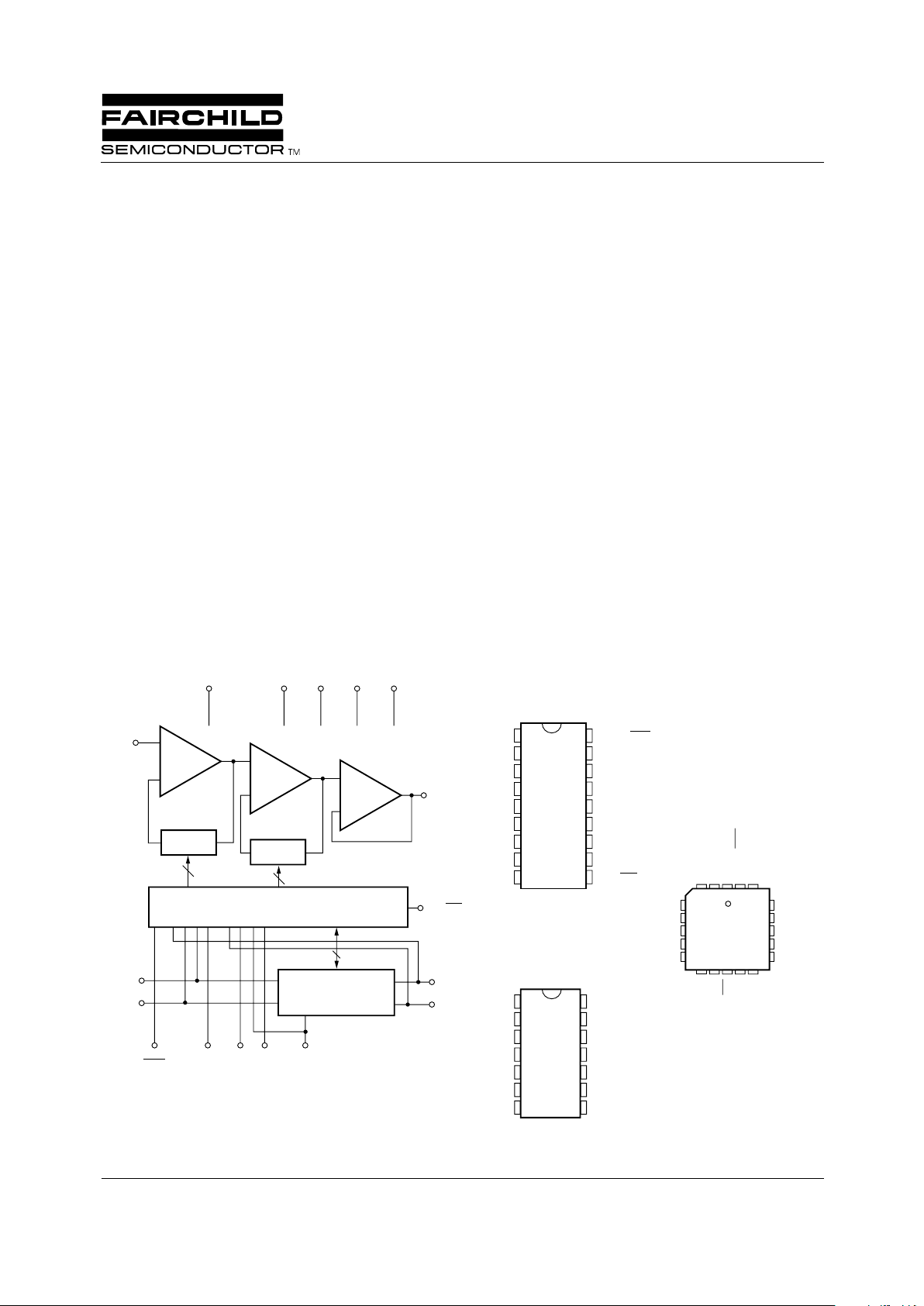
Block Diagram Pin Connections
V
OUT
V
IN
V
CC
PDNA GND VSSGND
+
16
16
C0
C1
F0
F2
9
C2
C3 F1 F3 F2
(SCK)
C2
(LATI)
ATTEN/
GAIN
C1
(SID)
C0
(LATO)
F0
(SOD)
–
C3
(LATI)C2
(SID)C1
C0 (LATO)
NC
P
DN
F3
F2 (SCK)
V
OUT
V
SS
A GND
NC
NC
(LATO)C0
P
DN
F3
(SCK)F2
F1
GND
C1 (SID)
F1
GND
SER/PAR
F0 (SOD)
V
IN
C2 (LATI)C3ATTEN/GAIN
V
CC
1
4
5
6
7
8
18
17
16
15
14
1201923
11 12 13109
2
3
4
5
6
7
8
9
18
17
16
15
14
13
12
11
10
ATTEN/GAIN
ML2003
18-PIN DIP
20-Pin PCC
ML2003
TOP VIEW
TOP VIEW
V
CC
V
OUT
V
SS
A GND
V
IN
NC
F0 (SOD)
SER/PAR
COURSE
DECODER/MODE SELECTOR
9-BIT LATCH &
SHIFT REGISTER
RESISTORS/
SWITCHES
NOTE: SERIAL MODE FUNCTIONS INDICATED BY PARENTHESES.
RESISTORS/
SWITCHES
+
–
FINE
+
–
BUFFER
SER/PAR
LATI
SID
LATO
P
DN
NC
SCK
GND
1
2
3
4
5
6
7
14
13
12
11
10
9
8
ML2004
14-PIN DIP
TOP VIEW
V
CC
V
OUT
V
SS
A GND
V
IN
NC
SOD
ML2003, ML2004
Logarithmic Gain/Attenuator
Page 2
ML2003, ML2004 PRODUCT SPECIFICATION
2
REV. 1.1.1 3/19/01
Pin Description
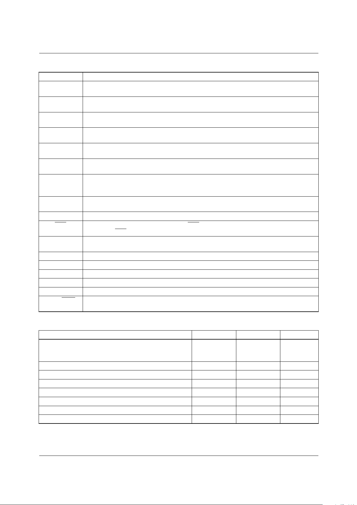
Absolute Maximum Ratings
1
Name Function
C3 In serial mode, pin is unused. In parallel mode, coarse gain select bit. Pin has internal pulldown
resistor to GND.
(LATI) C2 In serial mode, input latch clock which loads the data from the shift register into the latch.
In parallel mode, coarse gain select bit. Pin has internal pulldown resistor to GND.
(SID) C1 In serial mode, serial data input that contains serial 9 bit data word which controls the gain
setting. In parallel mode, coarse gain select bit. Pin has internal pulldown resistor to GND.
(LATO) C0 In serial mode, output latch clock which loads the 9 bit data word back into the shift register from
the latch. In parallel mode, coarse gain select bit. Pin has internal pulldown resistor to GND.
P
DN
Powerdown input . When P
DN
= 1, device is in powerdown mode. When P
DN
= 0, device is in
normal operation. Pin has internal pulldown resistor to GND.
F3 In serial mode, pin is unused. In parallel mode, fine gain select bit. Pin has internal pulldown
resistor to GND.
(SCK) F2 In serial mode, shift register clock which shifts the serial data on SID into the shift register on
rising edges and out on SOD on falling edges. In parallel mode, fine gain select bit. Pin has
internal pulldown resistor to GND.
F1 In serial mode, pin is unused. In parallel mode, fine gain select bit. Pin has internal pulldown
resistor to GND.
GND
Digital ground . 0 volts. All digital inputs and outputs are referenced to this ground.
SER/PAR Serial or parallel select input. When SER/PAR = 1, device is in serial mode.
When SER/PAR = 0, device is in parallel mode. Pin has internal pullup resistor to V
CC
.
(SOD) F0 In serial mode, serial output data which is the output of the shift register. In parallel mode, fine
gain select bit. Pin has internal pulldown resistor to GND.
V
IN
Analog input .
AGND
Analog ground . 0 volts. Analog input and output are referenced to this ground.
V
SS
Negative supply . –5 volts ±10%.
V
OUT
Analog output .
V
CC
Positive supply . +5 volts ±10%.
ATTEN/GAIN In serial mode, pin is unused. In parallel mode, attenuation/gain select bit. Pin has internal
pulldown resistor to GND.
Parameter Min. Max. Units
Supply Voltage
V
CC
V
SS
+6.5
-6.5
V
V
AGND with respect to GND ±0.5 V
Analog Input and Output V
SS
–0.3V V
CC
+0.3 V
Digital Input and Outputs GND –0.3 V
CC
+0.3 V
Input Current Per Pin ±25 mA
Power Dissipation 750 mW
Storage Temperature Range -65 +150 °C
Lead Temeperature (Soldering, 10 sec) 300 °C
Page 3
PRODUCT SPECIFICATION ML2003, ML2004
REV. 1.1.1 3/19/01
3
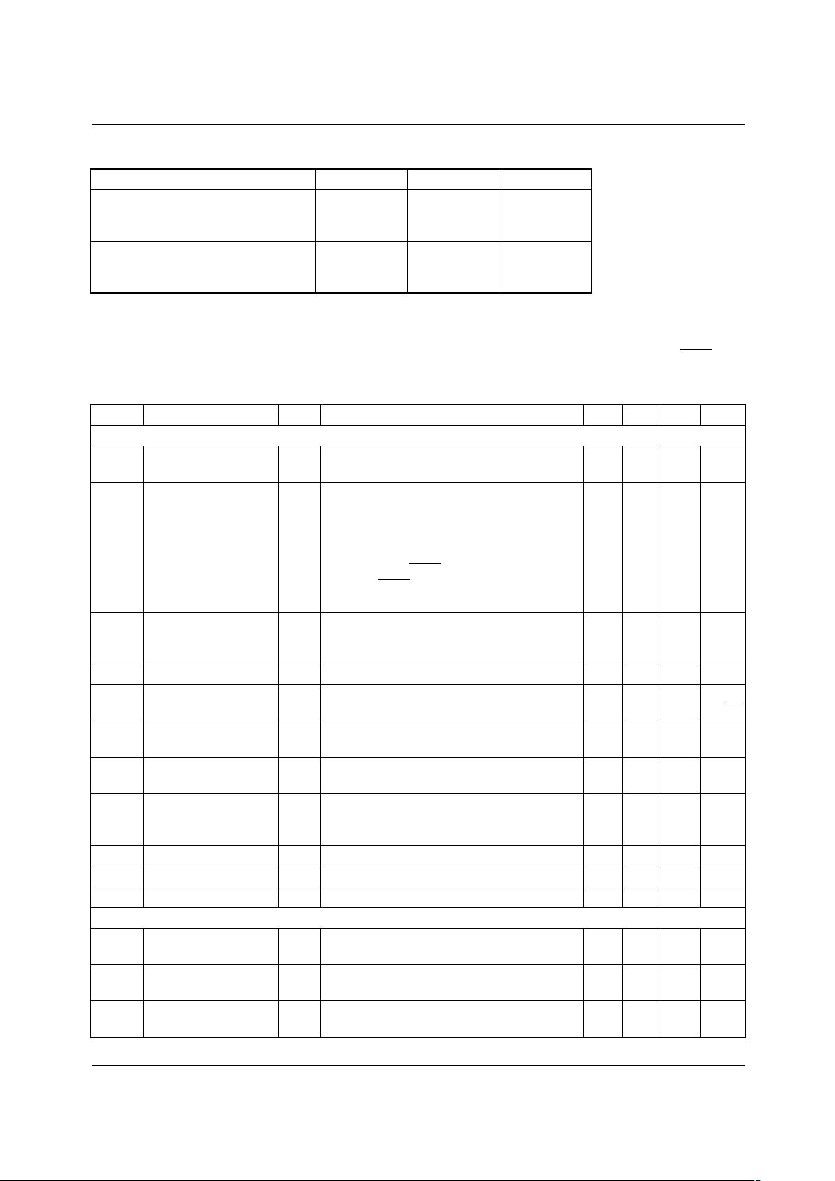
Operating Conditions
Parameter Min. Max. Units
Temperature Range
2
ML2003CX, ML2004CX
ML2003IX, ML2004IX
0
-40
70
85
°C
°C
Supply Voltage
V
CC
V
SS
4
-4
6
-6
V
V
Electrical Characteristics
Unless otherwise specified T
A
= T
MIN
to T
MAX
, V
CC
= 5V ± 10%, V
SS
= -5V ±10%, Data Word: ATTEN/GAIN
= 1,
Other Bits = 0(0dB Ideal Gain), C
L
= 100pF, R
L
= 600 Ω , SCK = LATI = LATO = 0, dBm measurements use 600 Ω as
reference load, digital timing measured at 1.4 V, C
L
= 100pF or SOD.
Symbol Parameter Notes Conditions Min. Typ.
3
Max. Units
Analog
AG Absolute gain
accuracy
4V
IN
=8dBm, 1 kHz -0.05 +0.05 dB
RG Relative gain
accuracy
4 100000001
000000000
000000001
All other gain settings
All values referenced to 100000000 gain
when ATTEN/GAIN = 1, V
IN
=8dBm when
ATTEN//GAIN =0
V
IN
=(8dBm – Ideal Gain) in dB
-0.05
-0.05
-0.05
-0.1
+0.05
+0.05
+0.05
+0.1
dB
dB
dB
dB
FR Frequency response 4 300-4000 Hz
100-20,000 Hz
Relative to 1 kHz
-0.05
-0.1
+0.05
+0.1dBdB
VOS Output Offset Voltage 4 V
IN
= 0, +24dB gain ±100 mV
ICN Idle Channel Noise 45V
IN
= 0, +24dB gain, C msg. Weighted
V
IN
= 0, +24dB gain, 1kHz
-6
4500 900
dBrnc
nv/ √ Hz
HD Harmonic Distortion 4 V
IN
= 8dBm gain, 1kHz Measure 2nd,
3rd harmonic relative to fundamental
-60 dB
SD Signal to Distortion 4 V
IN
= 8dBm, 1 kHz
C msg. weighted
+60 dB
PSRR Power Supply
Rejection
4 200mVp-p, 1 kHz sine, V
IN
= 0
on V
CC
on V
SS
-60
-60
-40
-40
dB
dB
Z
IN
Input impedance, V
IN
4 1 Meg
V
INR
Input Voltage Range 4 ±3.0 V
V
OSW
Output Voltage Swing 4 ±3.0 V
Digital and DC
V
IL
Digital Input Low
Voltage
4 0.8 V
V
IH
Digital Input High
Voltage
4 2.0 V
V
OL
Digital Output Low
Voltage
4I
OL
= 2mA 0.4 V
Page 4
ML2003, ML2004 PRODUCT SPECIFICATION
4
REV. 1.1.1 3/19/01
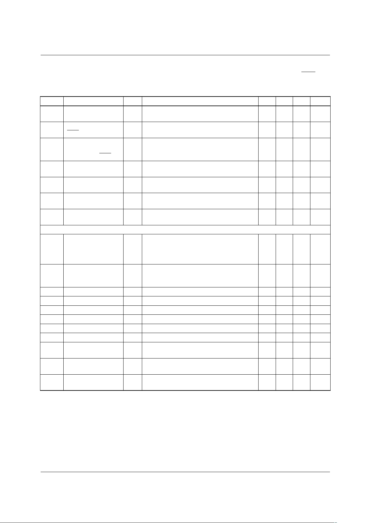
Notes:
1. Absolute maximum ratings are limits beyond which the life of the integrated circuit may be impaired. All voltages unless
otherwise specified are measured with respect to ground.
2. 0°C to +70°C and –40°C to +85°C operating temperature range devices are 100% tested with temperature limits guaranteed
by 100% testing, sampling, or by correlation with worst-case test conditions.
3. Typicals are parametric norm at 25°C.
4. Parameter guaranteed and 100% production tested.
5. Parameter guaranteed. Parameters not 100% tested are not in outgoing quality level calculation.
V
OH
Digital Output High
Voltage
4I
OH
= -1mA 4.0 V
I
NS
Input Current, SER/
PAR
4V
IH
= GND -5 -100 µA
I
ND
Input Current,
All Digital Inputs
Except SER/PER
4V
IH
= V
CC
5 100 µA
I
CC
V
CC
Supply Current 4 No output load, V
IL
= GND,
V
IH
= V
CC
, V
IN
= 0
4 mA
I
SS
V
SS
Supply Current 4 No output load, V
IL
= GND,
V
IH
= V
CC
, V
IN
= 0
-4 mA
I
CCP
V
CC
Supply Current,
Powerdown Mode
4 No output load, V
IL
= GND,
V
IH
= V
CC
0.5 mA
I
SSP
V
SS
Supply Current
Powerdown Mode
4 No output load, V
IL
= GND,
V
IH
= V
CC
-0.1 mA
AC Characteristics
t
SET
V
OUT
Settling Time 4 V
IN
= 0.185V. Change gain from –24 to
+24dB. Measure from LATI rising edge to
when V
OUT
settles to within 0.05dB of final
value.
20 µs
t
STEP
V
OUT
Step Response 4 Gain = +24dB. V
IN
= -0.185 to +0.185V
step. Measure when V
OUT
settles to within
0.05dB of final value.
20 µs
t
SCK
SCK On/Off Period 4 250 ns
t
S
SID Data Setup Time 4 50 ns
t
H
SID Data Hold Time 4 50 ns
t
D
SOD Data Delay 4 0 125 ns
t
IPW
LATI Pulse Width 4 50 ns
t
OPW
LATO Pulse Width 4 50 ns
tIS, tOSLATI, LATO Setup
Time
450ns
t
IH
,
t
OH
LATI, LATO Hold
Time
550ns
t
PLD
SOD Parallel Load
Delay
4 0 125 ns
Electrical Characteristics (continued)
Unless otherwise specified TA = T
MIN
to T
MAX
, VCC = 5V ± 10%, VSS = -5V ±10%, Data Word: ATTEN/GAIN = 1,
Other Bits = 0(0dB Ideal Gain), CL = 100pF, RL = 600Ω, SCK = LATI = LATO = 0, dBm measurements use 600Ω as
reference load, digital timing measured at 1.4 V, CL = 100pF or SOD.
Symbol Parameter Notes Conditions Min. Typ.3Max. Units
Page 5

PRODUCT SPECIFICATION ML2003, ML2004
REV. 1.1.1 3/19/01 5
Timing Diagram
Figure 1. Serial Mode Timing Diagram
SCK
t
SCK
t
SCK
t
S
t
IS
t
IH
t
OS
t
OH
t
IPW
t
OPW
t
PLD
t
D
t
H
SID
SOD
SCK
LATI
LATO
SOD
TIMING PARAMETERS ARE REFERENCED TO THE 1.4 VOLT MIDPOINT.
Typical Performance Curves
Figure 2. Amplitude vs Frequency (VIN/V
OUT
= .5V
RMS
) Figure 3. Amplitude vs Frequency (VIN/V
OUT
= 2V
RMS
)
0 0
-0.5
AMPLITUDE (dB)
FREQUENCY (Hz)
-0.10
-0.15
-0.20
-0.25
-0.30
-0.35
-0.40
-0.45
-0.50
100 1K 10K 100K
-0.5
AMPLITUDE (dB)
FREQUENCY (Hz)
-0.10
-0.15
-0.20
-0.25
-0.30
-0.35
-0.40
-0.45
-0.50
100 1K 10K 100K
ATTEN: VIN = 0.5V
RMS
GAIN: VIN = 0.5V
RMS
/GAIN SETTING
ATTEN: VIN = 2V
RMS
GAIN: VIN = 2V
RMS
/GAIN SETTING
GAIN = +24dB
GAIN = +18dB
GAIN = +12dB
GAIN = +0, -24dB
GAIN = +24dB
GAIN = 0dB
GAIN = –24dB
Page 6

ML2003, ML2004 PRODUCT SPECIFICATION
6 REV. 1.1.1 3/19/01
Figure 6. C
MSG
S/N vs Gain Setting Figure 7. Gain Error vs Gain Setting
C
MSG
S/N (dB)
GAIN SETTING (dB)
40
50
60
70
80
90
100
-24 -18 -12 -6 -0 6 12 18 24
GAIN ERROR (dB)
GAIN SETTING (dB)
0
0.02
-0.02
-0.04
-0.06
-0.08
-1.0
0.04
0.06
0.08
0.1
-24 -18 -12 -6 -0 6 12 18 24
ATTEN: VIN = 8dBm
GAIN: V
IN
= 8dBm/GAIN SETTING
1KHz
Figure 8. S/N + D vs Gain Setting (VIN/V
OUT
= 2V
RMS
) Figure 9. S/N + D vs Gain Setting (VIN/V
OUT
= 0.5V
RMS
)
80
70
60
50
40
30
20
10
-24 -18 -12 -6 0
GAIN SETTING (dB)
S/N + D (dB)
6121824
VIN = 1kHz
VIN = 20kHz
VIN = 50kHz
ATTEN: VIN = 2V
RMS
GAIN: VIN = 2V
RMS
/GAIN SETTING
S/N + D (dB)
GAIN SETTING (dB)
80
70
60
50
40
30
20
-24 -18 -12 -6 0 6 12 18 24
VIN = 1kHz
VIN = 20kHz
VIN = 50kHz
ATTEN: VIN = 0.5V
RMS
GAIN: VIN = 0.5V
RMS
/GAIN SETTING
Typical Performance Curves (continued)
Figure 4. Output Noise Voltage vs Frequency Figure 5. C
MSG
Output Noise vs Gain Settings
2.0
1.8
OUTPUT NOISE VOLTAGE (µV/√Hz)
C
MSG
OUTPUT (NOISE) (dBmc)
FREQUENCY (Hz) GAIN SETTING (dB)
1.6
1.4
1.2
1
0.8
0.6
0.4
0.2
0
10
-10
-9
-8
-7
-6
-5
-4
-3
-2
-24 -18 -12 -6 -0 6 12 18 24
100 1K 10K
GAIN = +24dB
V
IN
= 6
GAIN = -24dB
GAIN = +12dB
Page 7

PRODUCT SPECIFICATION ML2003, ML2004
REV. 1.1.1 3/19/01 7
Functional Description
The ML2003 consists of a coarse gain stage, a fine gain
stage, an output buffer, and a serial/parallel digital interface.
Gain Stages
The analog input, VIN, goes directly into the op amp input in
the coarse gain stage. The coarse gain stage has a gain range
of 0 to 22.5dB in 1.5dB steps.
The fine gain stage is cascaded onto the coarse section. The
fine gain stage has a gain range of 0 to 1.5dB in 0.1dB steps.
In addition, both sections can be programmed for either gain
or attenuation, thus doubling the effective gain range.
The logarithmic steps in each gain stage are generated by
placing the input signal across a resistor string of 16 series
resistors. Analog switches allow the voltage to be tapped
from the resistor string at 16 points. The resistors are sized
such that each output voltage is at the proper logarithimic
ratio relative to the input signal at the top of the string. Attenuation is implemented by using the resistor string as a simple
voltage divider, and gain is implemented by using the resistor string as a feedback resistor around an internal op amp.
Gain Settings
Since the coarse and fine gain stages are cascaded, their gains
can be summed logarithmically. Thus, any gain from –24dB to
+24dB in 0.1dB steps can be obtained by combining the
coarse and fine gain settings to yield the desired gain setting.
The relationship between the digital select bits and the corresponding analog gain values is shown in Tables 1 and 2. Note
that C3-C0 selects the coarse gain, F3-F0 selects the fine gain,
and ATTEN/GAIN
selects either attenuation or gain.
Output Buffer
The final analog stage is the output buffer. This amplifier has
internal gain of 1 and is designed to drive 600 ohms and
100pF loads. Thus, it is suitable for driving a telephone
hybrid circuit directly without any external amplifier.
Power Supplies
The digital section is powered between VCC and GND, or 5
volts. The analog section is powered between VCC and VSS
and uses AGND as the reference point, or ±5 volts.
GND and AGND are totally isolated inside the device to
minimize coupling from the digital section into the analog
section. However, AGND and GND should be tied together
physically near the device and ideally close to the common
power supply ground connection.
Typically, the power supply rejection of VCC and VSS to the
analog output is greater than –60dB at 1 kHz. If decoupling
of the power supplies is still necessary in a system, VCC and
VSS should be decoupled with respect to AGND.
Powerdown Mode
A powerdown mode can be selected with pin PDN. When
PDN = 1, the device is powered down. In this state, the power
consumption is reduced by removing power from the analog
section and forcing the analog output,V
OUT
, to a high
impedance state. While the device is in powerdown mode,
the digital section is still functional and the current data
word remains stored in the latch when in serial mode.
When PDN = 0, the device is in normal operation.
Digital Section
The ML2003 can be operated with a serial or parallel
interface. The SER/PAR pin selects the desired interface.
When SER/PAR = 1, the serial mode is selected. When
SER/PAR = 0, the parallel mode is selected. The ML2004
digital interface is serial only.
Serial Mode
Serial mode is selected by setting SER/PAR pin high. The
serial interface allows the gain settings to be set from a serial
data word.
The timing for the serial mode is shown in Figure 10. The
serial input data, SID, is loaded into a shift register on rising
edges of the shift clock, SCK. The data can be parallel
loaded into a latch when the input latch signal, LATI, is high.
The LATI pulse must occur when SCK is low. In this way,
a new data word can be loaded into the shift register without
disturbing the existing data word in the latch.
The parallel outputs of the latch control the attenuation/gain
setting. The order of the data word bits in the latch is shown
in Figure 11. Note that bit 0 is the first bit of the data word
clocked into the shift register. Tables 1 and 2 describe how
the data word programs the gain.
Table 1. Fine Gain Settings (C3-C0 = 0)
F3 F2 F1 F0
Ideal Gain (dB)
ATTEN/GAIN = 1 ATTEN/GAIN = 0
0
0
0
0
0
0
0
0
1
1
1
1
1
1
1
1
0
0
0
0
1
1
1
1
0
0
0
0
1
1
1
1
0
0
1
1
0
0
1
1
0
0
1
1
0
0
1
1
0
1
0
1
0
1
0
1
0
1
0
1
0
1
0
1
0
-.1
-.2
-.3
-.4
-.5
-.6
-.7
-.8
-.9
-1.0
-1.1
-1.2
-1.3
-1.4
-1.5
0
.1
.2
.3
.4
.5
.6
.7
.8
.9
1.0
1.1
1.2
1.3
1.4
1.5
Page 8

ML2003, ML2004 PRODUCT SPECIFICATION
8 REV. 1.1.1 3/19/01
Table 2. Coarse Gain Settings (F3-F0 = 0)
The device also has the capability to read out the data word
stored in the latch. This can be done by parallel loading the
data from the latch back into the shift register when the latch
signal, LATO, is high. The LATO pulse must occur when
SCK is low. Then, the data word can be shifted out of the
shift register serially to the output, SOD, on falling edges of
the shift clock, SCK.
The loading and reading of the data word can be done
continuously or in burst. Since the shift register and latch
circuitry inside the device is static, there are no minimum
frequency requirements on the clocks or data pulses.
However, there is coupling (typically less than 100µV) of
the digital signals into the analog section. This coupling
can be minimized by clocking the data bursts in during
noncritical intervals or at a frequency outside the analog
frequency range.
Parallel Mode
The parallel mode is selected by setting SER/PAR pin low.
The parallel interface allows the gain settings to be set with
external switches or from a parallel microprocessor interface.
In parallel mode, the shift register and latch are bypassed and
connections are made directly to the gain select bits with
external pins ATTEN/GAIN
, C3-C0, and F3-F0. Tables 1
and 2 describe how these pins program the gain. The pins
ATTEN/GAIN, C3-C0, and F3-F0 have internal pulldown
resistors to GND. The typical value of these pulldown
resistors is 100kΩ.
C3 C2 C1 C0
Ideal Gain (dB)
ATTEN/GAIN
= 1 ATTEN/GAIN = 0
0
0
0
0
0
0
0
0
1
1
1
1
1
1
1
1
0
0
0
0
1
1
1
1
0
0
0
0
1
1
1
1
0
0
1
1
0
0
1
1
0
0
1
1
0
0
1
1
0
1
0
1
0
1
0
1
0
1
0
1
0
1
0
1
0
-1.5
-3.0
-4.5
-6.0
-7.5
-9.0
-10.5
-12.0
-13.5
-15.0
-16.5
-18.0
-19.5
-21.0
-22.5
0
1.5
3.0
4.5
6.0
7.5
9.0
10.5
12.0
13.5
15.0
16.5
18.0
19.5
21.0
22.5
Figure 10. Serial Mode Timing
SCK
SCK
01234 5 6 78
0123 4 567 8
a) LOAD
b) READ
SID
SID
LATI
LATI
LATO
LATO
SOD
SOD
F0 F1 F2 F3 C0 C1 C2 C3
ATT/
GAIN
F0 F1 F2 F3 C0 C1 C2 C3
ATT/
GAIN
Page 9

PRODUCT SPECIFICATION ML2003, ML2004
REV. 1.1.1 3/19/01 9
Figure 11. 9-Bit Latch
Applications
Figure 12. Typical Serial Interface Figure 13. Typical µP Parallel Interface
Figure 14. Controlling Multiple ML2004 with Only 3 Digital Lines Using One Long Data Word
Figure 15. AGC for DSP or Modem Front End
87 654321 0
MSB LSB
F0F1F2F3C0C1C2C3ATTEN/GAIN
FUNCTION
BIT NUMBER
ML2004
LOG GAIN/ATTEN
ML2021
EQUALIZER
V
IN
V
OUT
µP
V
IN
SID
SCK
LATI
SID
SCK
LATI
V
OUT
ML2003
8-BIT LATCH
ATTEN/GAIN
C3-C0
F3-F1
µP
V
IN
V
OUT
µP
ML2004
V
IN
V
OUT
SID
SCK
LATI
SOD
ML2004
V
IN
V
OUT
SID
SCK
LATI
SOD
ML2004
V
IN
V
OUT
SID
SCK
LATI
SOD
ML2003
ATTEN/GAIN
C3-C0
F3-F1
A/D
V
IN
V
IN
µP
OR
DSP
V
IN
V
OUT
8-BIT LATCH
Page 10

ML2003, ML2004 PRODUCT SPECIFICATION
10 REV. 1.1.1 3/19/01
Figure 16. Analog AGC
Figure 17. Digitally Controlled Volume Control
Figure 18. Precision Peak Detector (±1%) with Controllable Acquire and Hold Time
ML2003
ATTEN/GAIN
C3-C0
F3-F1
V
IN
V
OUT
UP/DOWN
8-BIT COUNTER
COMPARATOR
CLOCK
U/D
–
+
+5
+5
R
1
R
3
R
2
R1, R2, R3 SETS AGC THRESHOLD
AND HYSTERESIS
ML2003
ATTEN/GAIN
C3-C0
F3-F1
V
IN
V
OUT
UP/DOWN
8-BIT CTR
CLOCK
DOWN UP
FROM
µP OR
SWITCHES
U/D
V
IN
V
REF
V
OUT
V
PEAK
V
PEAK
ML2003
ATTEN/GAIN
C3-C0
F3-F1
V
IN
V
OUT
UP/DOWN
8-BIT COUNTER
COMPARATOR
CLK1 CLK2
U/D
–
+
f
CLK1
DETERMINES PEAK ACQUIRE TIME
f
CLK2
DETERMINES PEAK HOLD TIME
Page 11

ML2003, ML2004 PRODUCT SPECIFICATION
3/19/01 0.0m 003
Stock#DS300042003
2001 Fairchild Semiconductor Corporation
LIFE SUPPORT POLICY
FAIRCHILD’S PRODUCTS ARE NOT AUTHORIZED FOR USE AS CRITICAL COMPONENTS IN LIFE SUPPORT DEVICES
OR SYSTEMS WITHOUT THE EXPRESS WRITTEN APPROVAL OF THE PRESIDENT OF FAIRCHILD SEMICONDUCTOR
CORPORATION. As used herein:
1. Life support devices or systems are devices or systems
which, (a) are intended for surgical implant into the body,
or (b) support or sustain life, and (c) whose failure to
perform when properly used in accordance with
instructions for use provided in the labeling, can be
reasonably expected to result in a significant injury of the
user.
2. A critical component in any component of a life support
device or system whose failure to perform can be
reasonably expected to cause the failure of the life support
device or system, or to affect its safety or effectiveness.
www.fairchildsemi.com
DISCLAIMER
FAIRCHILD SEMICONDUCTOR RESERVES THE RIGHT TO MAKE CHANGES WITHOUT FURTHER NOTICE TO
ANY PRODUCTS HEREIN TO IMPROVE RELIABILITY, FUNCTION OR DESIGN. FAIRCHILD DOES NOT ASSUME
ANY LIABILITY ARISING OUT OF THE APPLICATION OR USE OF ANY PRODUCT OR CIRCUIT DESCRIBED HEREIN;
NEITHER DOES IT CONVEY ANY LICENSE UNDER ITS PATENT RIGHTS, NOR THE RIGHTS OF OTHERS.
Ordering Information
Part Number Temperature Range Package
ML2003IQ -40°C to 85°C Molded PCC (Q20)
ML2003CP 0°C to 70°C Molded DIP (P18)
ML2003CQ 0°C to 70°C Molded PCC (Q20)
ML2004IP -40°C to 85°C Molded DIP (P14)
ML2004CP 0°C to 70°C Molded DIP (P14)
 Loading...