

Page 1
www.lansdale.comPage 1 of 24 Issue 0
ML145162
60 MHz and 85 MHz Universal
Programmable Dual PLL Frequency
Synthesizers
CMOS
Legacy Device: Motorola MC145162
The ML145162 is a dual phase–locked loop (PLL) frequency synthesizer
especially designed for CT–1 cordless phone applications worldwide. This
frequency synthesizer is also for any product with a frequency operation at
60MHz or below.
The device features fully programmable receive, transmit, reference, and
auxiliary reference counters accessed through an MCU serial interface. This
feature allows this device to operate in any CT–1 cordless phone application.
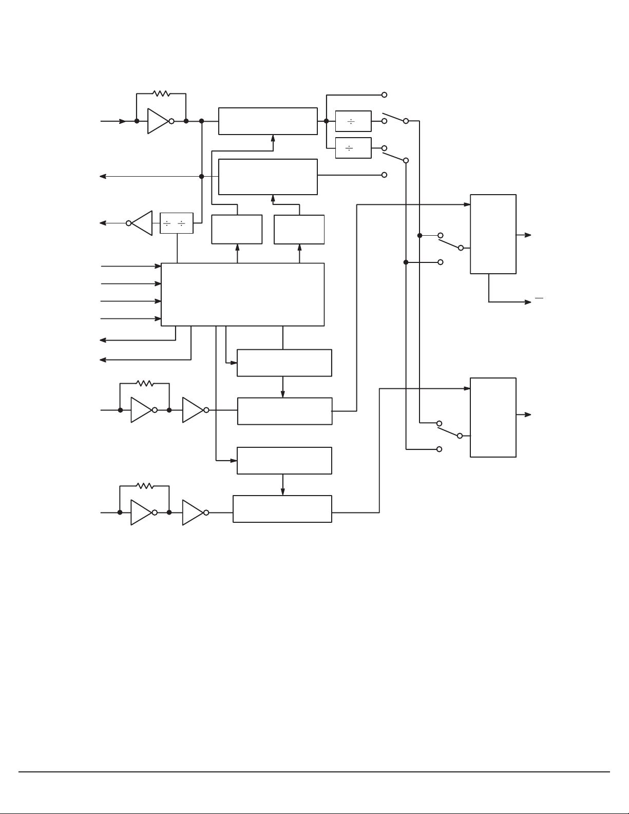
The device consists of two independent phase detectors for transmit and
receive loops. A common reference oscillator, driving two independent reference frequency counters, provides independent reference frequencies for
transmit and receive loops. The auxiliary reference counter allows the user to
select an additional reference frequency for receive and transmit loops if
required.
• Operating Voltage Range: 2.5 to 5.5 V
• Operating Temperature Range: TA= – 40 to +75°C
• Operating Power Consumption: 3.0 mA @ 2.5 V
• Maximum Operating Frequency: 60 MHz @ 200 mV p–p, VDD= 2.5 V
• Three or Four Pins Used for Serial MCU Interface
• Built–In MCU Clock Output with Frequency of Reference Oscillator ÷3/÷4
• Power Saving Mode Controlled by MCU
• Lock Detect Signal
• On–Chip Reference Oscillator Supports External Crystals to 16.0 MHz
• Reference Frequency Counter Division Range: 16 to 4095
• Auxiliary Reference Frequency Counter Division Range: 16 to 16,383
• Transmit Counter Division Range: 16 to 65,535
• Receive Counter Division Range: 16 to 65,535
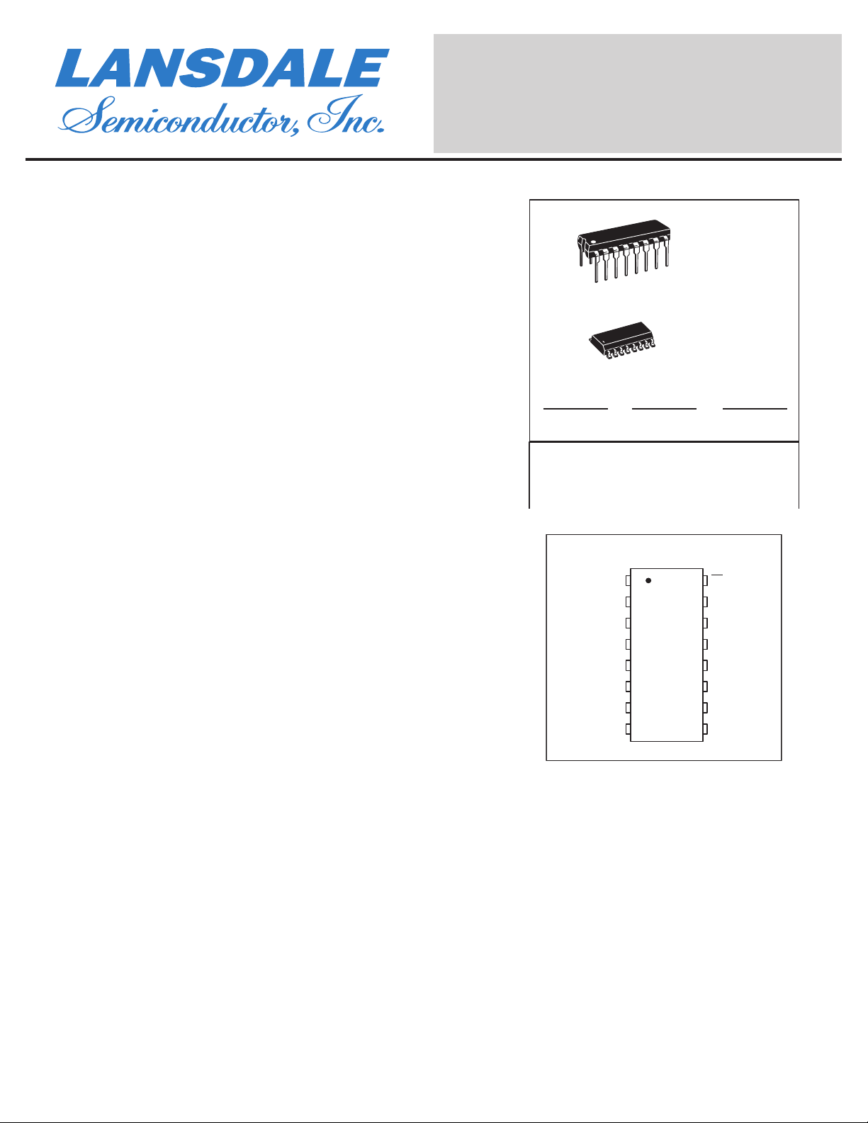
P DIP 16 = EP
PLASTIC DIP
16
1
16
1
CROSS REFERENCE/ORDERING INFORMATION
MOTOROLA
P DIP 16 MC145162P ML145162EP
SOG 16 MC145162D ML145162-5P
Note: Lansdale lead free (Pb) product, as it
becomes available, will be identified by a part
number prefix change from ML to MLE.
PIN ASSIGNMENT
1
CLK
2
AD
in
3
D
in
ENB
4
MCUCLK
V
6
SS
out
7
in
8
OSC
OSC
CASE 648
SOG 16 = -5P
SOG PACKAGE
CASE 751B
LANSDALEPACKAGE
16
LD
15
TxPD
out
14
fin–T
13
TxPS/f
Tx
125
V
DD
11
RxPS/F
Rx
10
RxPD
out
9
fin–R
Page 2
www.lansdale.comPage 2 of 24 Issue 0
LANSDALE Semiconductor, Inc.
ML145162
BLOCK DIAGRAM
OSC
OSC
out
A
f
R1
25
B
4
C
f
R2
D
7
in
8
12–BIT PROGRAMMABLE
REFERENCE COUNTER
14–BIT PROGRAMMABLE
AUXILIARY REFERENCE
COUNTER
MCUCLK
AD
in
CLK
D
in
ENB
TxPS/f
Tx
RxPS/f
Rx
fin–T
fin–R
5
2
1
3
4
13
11
14
9
3/ 4
12–BIT SHIFT
REGISTER
MCU INTERFACE PROGRAMMING
MODE CONTROL
CONTROL REGISTER
16–BIT SHIFT REGISTER
16–BIT Tx PROGRAMMABLE
16–BIT SHIFT REGISTER
16–BIT Rx PROGRAMMABLE
COUNTER
14–BIT SHIFT
REGISTER
COUNTER
TRANSMIT
SELECT
RECEIVE
SELECT
VDD = PIN 12
VSS = PIN 6
Tx
PHASE
DETECTOR
Rx
PHASE
DETECTOR
15
16
10
TxPD
LD
RxPD
out
out
Page 3
www.lansdale.comPage 3 of 24 Issue 0
LANSDALE Semiconductor, Inc.
ML145162
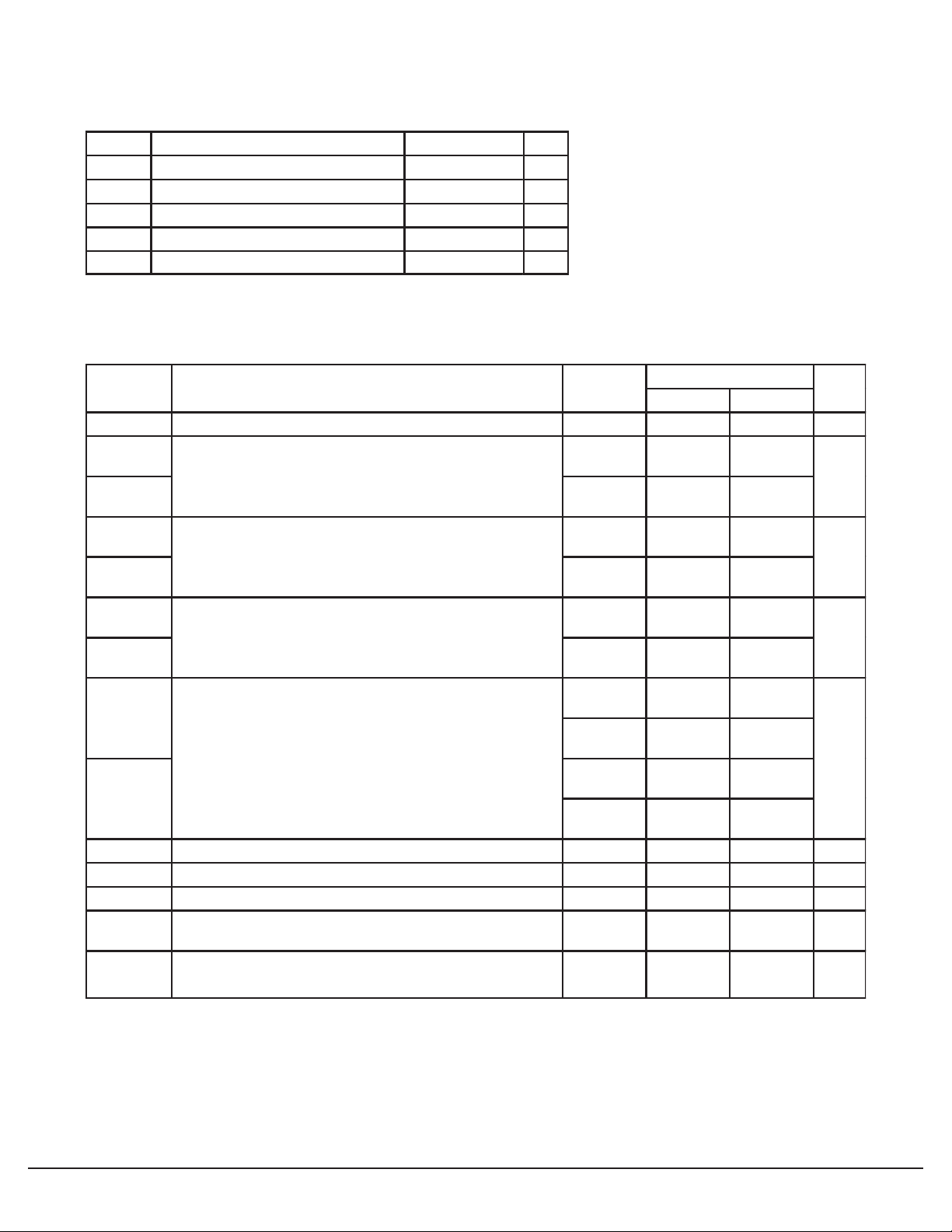
MAXIMUM RATINGS* (Voltages Referenced to V
Symbol Rating Value Unit
V
V
Iin, I
IDD, ISSDC Current Drain VDD or VSS Pins 30 mA
T
* Maximum Ratings are those values beyond which damage to the device may occur.
Functional operation should be restricted to the limits in the Electrical Characteristics
tables or Pin Descriptions section.
DC Supply Voltage – 0.5 to + 6.0 V
DD
Input Voltage, All Inputs – 0.5 to VDD + 0.5 V
in
DC Current Drain Per Pin 10 mA
out
Storage Temperature Range – 65 to + 150 °C
stg
ELECTRICAL CHARACTERISTICS (Voltages Referenced to V
Symbol Characteristic V
V
DD
V
OL
V
OH
V
IL
V
IH
I
OH
I
OL
I
IL
I
IH
I
OZ
C
in
C
out
I
DD(stdby)
I
DD
Power Supply Voltage Range — 2.5 5.5 V
Output Voltage 0 Level
(I
=0)
out
(Vin=VDD or 0) 1 Level 2.5
Input Voltage 0 Level
(V
= 0.5 V or VDD– 0.5 V)
out
Output Current (V
Input Current OSCin, fin–T, fin–R
(Vin=0)
(Vin=VDD– 0.5) OSCin, fin–T, fin–R 2.5
Three–State Leakage Current (V
Input Capacitance — — 8.0 pF
Output Capacitance — — 8.0 pF
Standby Current
(All Counters are in Power–Down Mode with Oscillator On)
Operating Current
ML145162: 200 mV p–p input at fin–T and fin–R = 60 MHz
= 2.2 V) Source
out
(V
= 5.0 V)
out
(V
= 0.3 V) Sink
out
(V
= 0.5 V)
out
)
SS
, TA = 25°C)
SS
1 Level 2.5
ADin, CLK, Din, ENB 2.5
ADin, CLK, Din, ENB 2.5
= 0 V or 5.5 V) 5.5 — ± 100 nA
out
This device contains protection circuitry to
guard against damage due to high static voltages or electric fields. However, precautions
must be taken to avoid application of any voltage
higher than maximum rated voltages to this
high–impedance circuit. For proper operation,
Vin and V
VSS≤ (Vin or V
Unused pins must always be tied to an
appropriate logic voltage level (e.g., either V
or VDD). Unused outputs must be left open.
DD
2.5
5.5
5.5
2.5
5.5
5.5
2.5
5.5
2.5
5.5
2.5
5.5
5.5
5.5
5.5
2.5
5.5
2.5 — 3.0
should be constrained to the range
out
) ≤ VDD.
out
Guaranteed Limit
Min Max
—
—
2.45
5.45
—
—
1.75
3.85
– 0.18
– 0.55
0.18
0.55
—
—
—
—
—
—
—
—
—
—
– 1.0
– 1.0
0.1
0.1
—
—
0.75
1.65
—
—
—
—
—
—
– 30
– 66
30
66
5.0
5.0
0.3
1.5
Unit
mA
mA
mA
SS
V
V
µA
Page 4
www.lansdale.comPage 4 of 24 Issue 0
LANSDALE Semiconductor, Inc.
ML145162
Figure
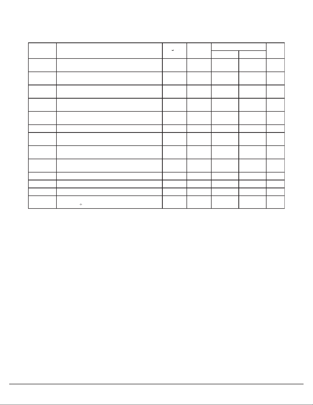
SWITCHING CHARACTERISTICS (T
Symbol Characteristic
t
TLH
t
THL
tr, t
t
w
f
max
t
st
t
su
t
h
t
rec
t
su1
t
h1
f Phase Detector Frequency dc 12.5 kHz
f
MCUCLK
Output Rise Time 1 2.5
Output Fall Time 1 2.5
Input Rise and Fall Time OSC
f
Input Pulse Width CLK and ENB 3 2.5
Input Frequency OSC
Input = Sine Wave @ ≥ 200 mV p–p fin–R, fin–T
Minimum Start–Up Time 10 ms
Setup Time DATA to CLK
Hold Time CLK to DATA 5 3.0
Recovery Time ENB to CLK 5 3.0
Setup Time ENB to CLK 4 2.5 – 5.5 80 — ns
Hold Time CLK to ENB 4 2.5 – 5.5 600 — ns
Output Clock Frequency MCUCLK
(OSCin 3)
= 25°C, CL = 50 pF)
A
ENB to CLK
Figure
No.
in
in
2 2.5
5 2.5
V
DD
5.5
5.5
5.5
5.5
2.5 – 5.5
2.5 – 5.5
5.5
5.0
5.0
Guaranteed Limit
Min Max
—
—
—
—
—
—
80
60
—
—
100
200
80
40
80
40
dc 5.33 MHz
200
100
200
100
5.0
4.0
—
—
16
60
—
—
—
—
—
—
Unit
ns
ns
µs
ns
MHz
ns
ns
ns
Page 5
www.lansdale.comPage 5 of 24 Issue 0
LANSDALE Semiconductor, Inc.
ML145162
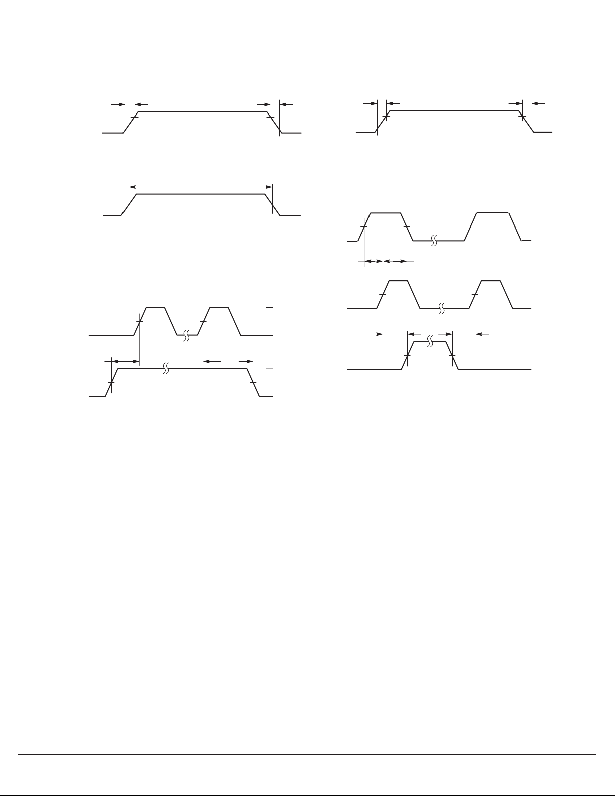
SWITCHING WAVEFORMS
ANY
OUTPUT
ENB, CLK
CLK
ENB
t
su1
t
TLH
10%
50%
t
r
90%
10%
90%
t
THL
CLK, OSCin,
fin–T, fin–R
Figure 1. Figure 2.
t
w
ADin,
D
in
50%
Figure 3.
t
su
FIRST
CLK
LAST
CLK
CLK
V
DD
V
SS
t
h1
V
DD
V
SS
ENB
50%
t
su
LAST
CLK
t
h
50%
PREVIOUS
DATA
LATCHED
FIRST
CLK
t
rec
t
f
V
DD
V
SS
V
DD
V
SS
V
DD
V
SS
Figure 4. ENB High During Serial Transfer
Figure 5. ENB Low During Serial Transfer
Page 6
www.lansdale.comPage 6 of 24 Issue 0
LANSDALE Semiconductor, Inc.
ML145162
PIN DESCRIPTIONS
INPUT PINS
OSCin/OSC
out
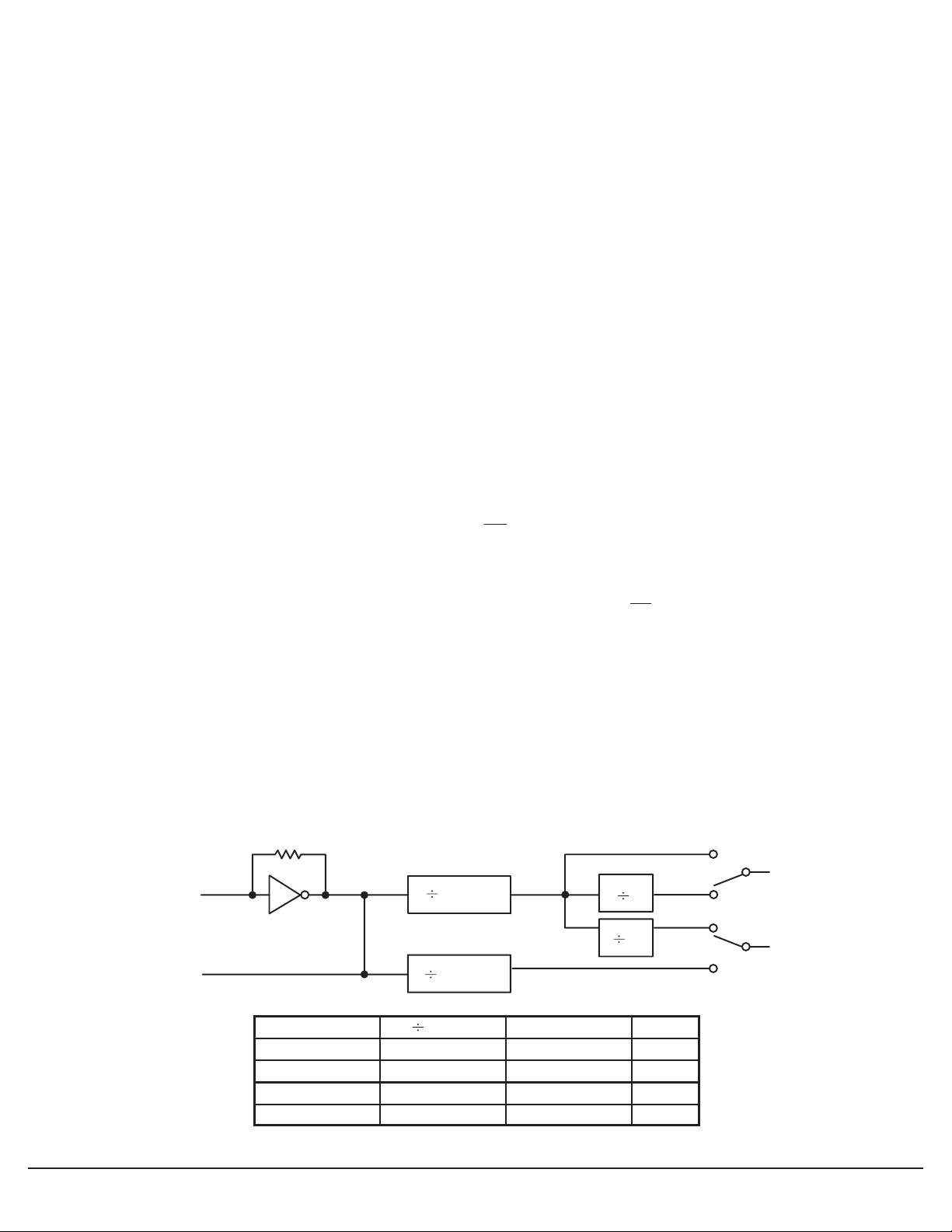
Reference Oscillator Input/Output (Pins 7, 8) These pins
form a reference oscillator when connected to an external parallel–resonant crystal. Figure 6 shows the relationship of different crystal frequencies and reference frequencies for cordless phone applications in various countries. OSCinmay also
serve as input for an externally generated reference signal
which is typically AC coupled.
MCUCLK
System Clock (Pin 5)
This output pin provides a signal of the crystal frequency
(OSC
out
) divided by 3 or 4 that is controlled by a bit in the
control register.
This signal can be a clock source for the MCU or other system clocks.
ADin,Din, CLK, ENB
Auxiliary Data In, Data In, Clock, Enable (Pins 2, 3, 1, 4)
These four pins provide an MCU serial interface for programming the reference counter, the transmit–channel counter, and the receive–channel counter. They also provide various
controls of the PLL including the power saving mode and the
programming format.
TxPS/fTx, RxPS/f
Rx
Transmit Power Save, Receive Power Save (Pins 13, 11)
For a normal application, these output pins provide the status
of the internal power saving mode operation. If the
transmit–channels counter circuitry is in power down mode,
TxPS/fTxoutputs a high state. If the receive–channels counter
circuitry is in power down mode, RxPS/fRxis set high. These
outputs can be applied for controlling the external power
switch for the transmitter and the receiver to save MCU control
pins.
In the Tx/Rx channel counter test mode, the TxPS/fTxand
RxPS/fRxpins output the divided value of the transmit channel
counter (fTx) and the receive channel counter (fRx), respectively. This test mode operation is controlled by the control
register. Details of the counter test mode are in the Tx/Rx
Channel Counter Test section of this data sheet.
fin–T/fin–R
Transmit/Receive Counter Inputs (Pins 14, 9)
fin–T and fin–R are inputs to the transmit and the receive
counters, respectively. These signals are typically driven from
the loop VCO and AC coupled. The minimum input signal
level is 200 mV p–p @ 60.0 MHz.
OUTPUT PINS
TxPD
out
/RxPD
out
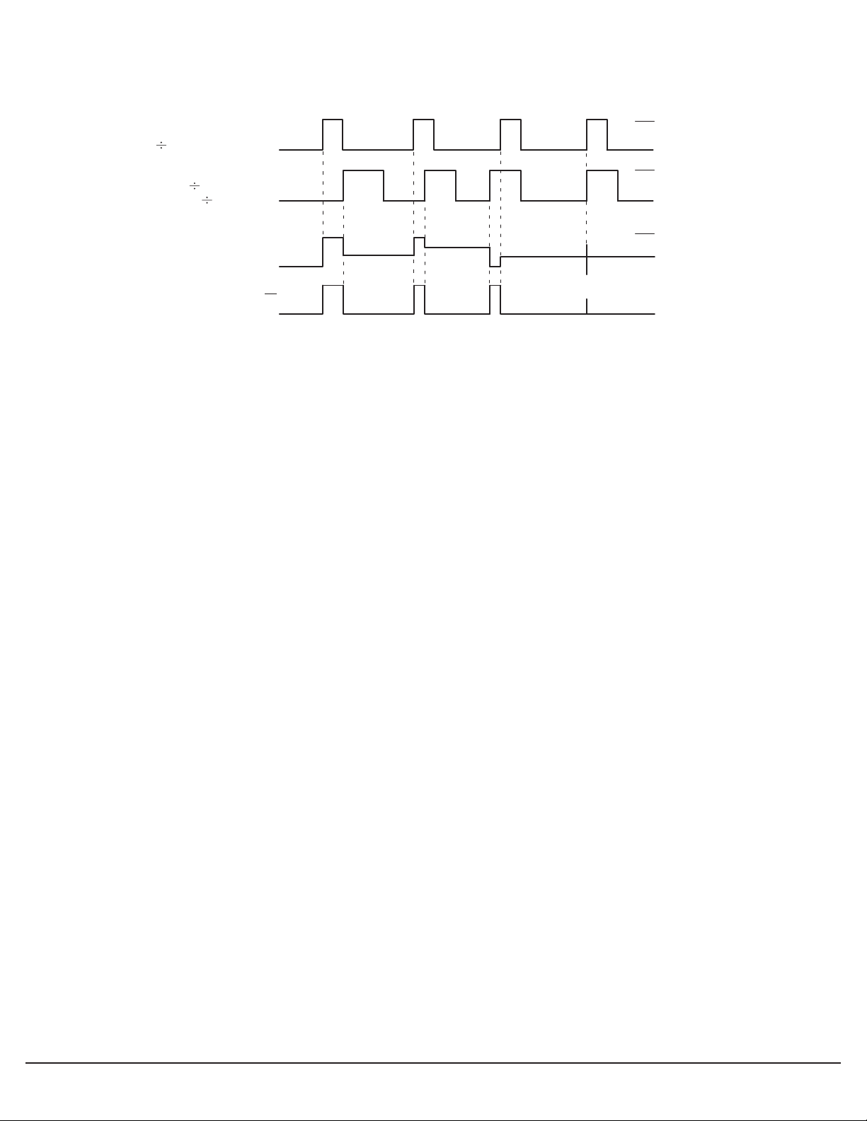
Transmit/Receive Phase Detector Outputs (Pins 15, 10)
These are three–state outputs of the transmit and receive
phase detectors for use as loop error signals (see Figure 7 for
phase detector output wave forms). Phase detector gain
isVDD/4 π volts per radian.
Frequency fV> fRor fVleading: output = negative pulse.
Frequency fV< fRor fVlagging: output = positive pulse.
Frequency fV= fRand phase coincidence: output = high–
impedance state.
NOTE: fRis the divided–down reference frequency at the
phase detector input and fVis the divided–down VCO frequency at the phase detector input.
LD
Lock Detect (Pin 16)
The lock detect signal is associated with the transmit loop.
The output at a high level indicates an out–of–lock condition
(see Figure 7 for the LD output wave form).
POWER SUPPLY
V
DD
Positive Power Supply (Pin 12)
VDDis the most positive power supply potential ranging
from 2.5 to 5.5 V with respect to VSS.
V
SS
Negative Power Supply (Pin 6)
VSSis the most negative supply potential and is usually connected to ground.
OSC
OSC
in
out
N (12 BITS)
M (14 BITS)
A
f
f
R1
R2
4
25
B
C
D
Crystal
11.150 MHz 446 6.25 kHz 1.0 kHz
11.150 MHz 223 12.5 kHz
10.240 MHz 512 5.0 kHz
12.000 MHz 600 5.0 kHz
Figure 6. Reference Frequencies for Cordless Phone Applications of Various Countries
N Value
f
R1→B
f
R2→C
Page 7
www.lansdale.comPage 7 of 24 Issue 0
MCU PROGRAMMING SCHEME
The MCU programming scheme is defined in two formats
controlled by the ENB input. If the enable signal is high during
the serial data transfer, control register/reference frequency
programming is selected. If the ENB is low, programming of
the transmit and receive counters is selected. During programming of the transmit and receive counters, both ADinand D
in
pins can input the data to the transmit and receive counters.
Both counters’ data is clocked into the PLL internal shift register at the leading edge of the CLK signal. It is not necessary to
reprogram the reference frequency counter/control register
when using the enable signal to program the transmit/receive
channels.
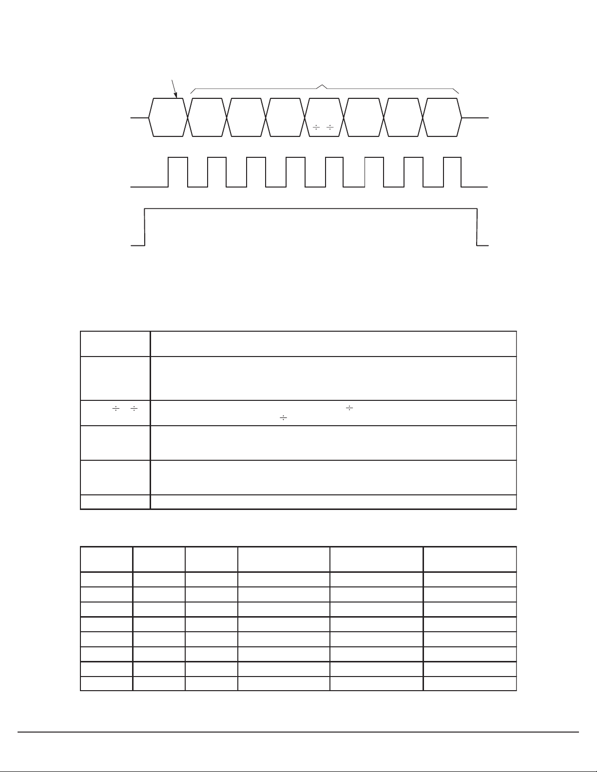
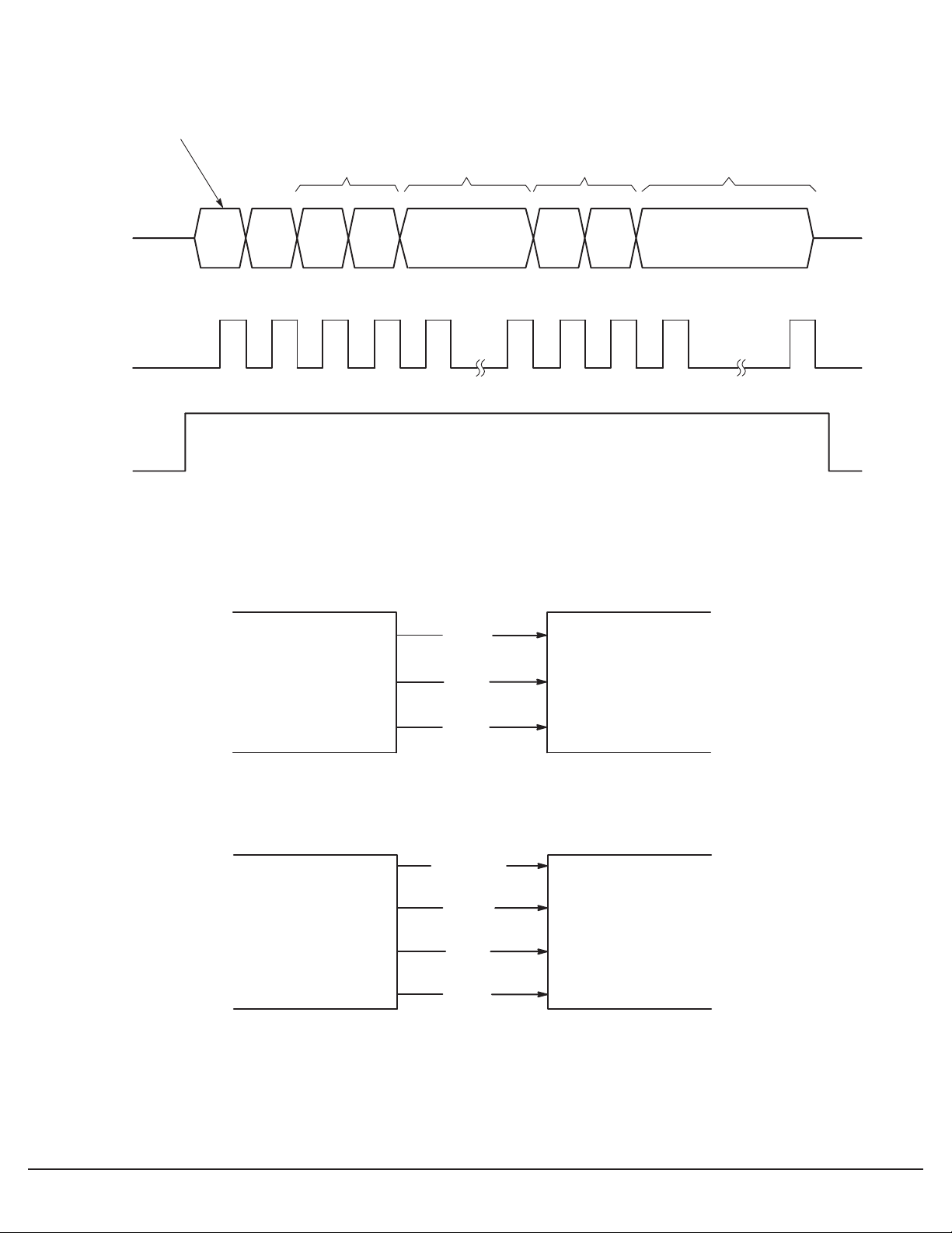
In programming the control register/reference frequency
scheme, the most significant bit (MSB) of the programming
word identifies whether the input data is the control word or
the reference frequency data word. If the MSB is 1, the input
data is the control word (Figure 8). Also see Figure 8 and Table
1 for control register and bit function. If the MSB is 0, the
input data is the reference frequency (Figure 9).
The reference frequency data word is a 32–bit word containing the 12–bit reference frequency data, the 14–bit auxiliary
reference frequency counter information, the reference frequency selection plus, the auxiliary reference frequency counter enable bit (Figure 9).
If the AUX REF ENB bit is high, the 14–bit auxiliary reference frequency counter provides an additional phase reference
frequency output for the loops. If AUX REF ENB bit is low,
the auxiliary reference frequency counter is forced into
power–down mode for current saving. (Other power down
modes are also provided through the control register per Table
2 and Figure 8.) At the falling edge of the ENB signal, the data
is stored in the registers.
There are two interfacing schemes for the universal channel
mode: the three–pin and the four–pin interfacing schemes. The
three–pin interfacing scheme is suited for use with the MCU
SPI (serial peripheral interface) (Figure 10), while the four–pin
interfacing scheme is commonly used for general I/O port connection (Figure 11).
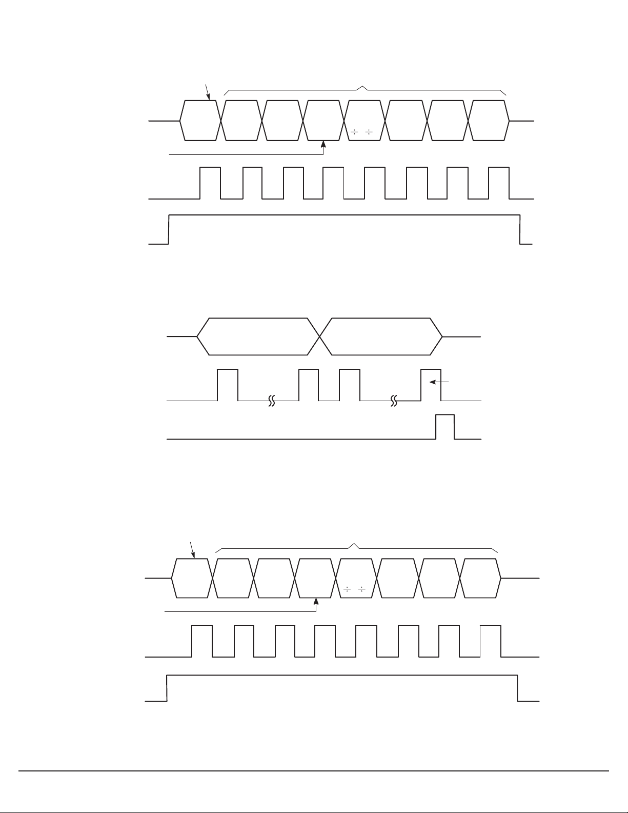
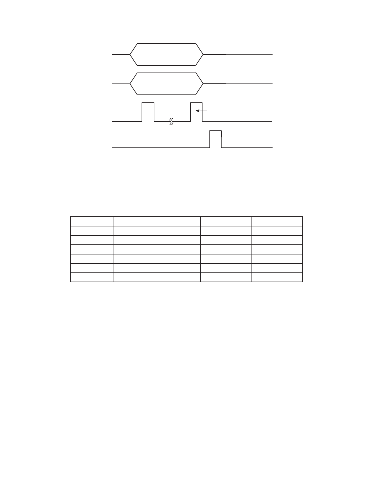
For the three–pin interfacing scheme, the auxiliary data
select bit is set to 0. All 32 bits of data, which define both
the16–bit transmit counter and the 16–bit receive counter, latch
into the PLL internal register through the data in pins at the
leading edge of CLK. See Figures 12 and 13.
For the four–pin interfacing scheme, the auxiliary data select
bit is set to 1. In this scheme, the 16–bit transmit counter’s data
enters into the ADinpin at the same time as the 16–bit receive
counter’s data enters into the Dinpin. This simultaneous entry
of the transmit and receive counters causes the programming
period of the four–pin scheme to be half that of the three–pin
scheme (see Figures 14 and 15).
While programming Tx/Rx Channel Counter, the ENB pin
must be pulsed to provide falling edge to latch the shifted data
after the rising edge of the last clock. Maximum data transfer
rate is 500 kbps.
NOTE
10 ms should be allowed for initial start–up time for
the oscillator to allow all registers to clear and enable
programming of new register values.
LANSDALE Semiconductor, Inc.
ML145162
fR, REFERENCE
(OSC
REFERENCE COUNTER)
in
fV, FEEDBACK
(fin–T
Tx COUNTER OR
fin–R
Rx COUNTER)
TxPD
out
OR
RxPD
out
LD
VH= High voltage level.
VL= Low voltage level.
*At this point, when both fR and fV are in phase, the output is forced to near mid supply.
NOTE: The TxPD
quency, the output is high impedance and the voltage at that pin is determined by the low–pass filter capacitor.
and RxPD
out
Figure 7. Phase Detector/Lock Detector Output Waveforms
generate error pulses during out–of–lock conditions. When locked in phase and fre-
out
V
H
V
L
V
H
V
L
*
V
H
HIGH IMPEDANCE
Page 8
www.lansdale.comPage 8 of 24 Issue 0
LANSDALE Semiconductor, Inc.
ML145162
CONTROL REGISTER IDENTIFIER = 1
D
in
CLK
ENB
NOTE: ENB must be high during the serial transfer.
10
MSB LSB
TEST
BIT
CONTROL REGISTER DATA
AUX
DATA
SELECT
REF
OUT
3/ 4
TxPD
ENABLE
RxPD
ENABLE
REF PD
ENABLE
Figure 8. Programming Format of the Control Register
Table 1. Control Register Function Bits Description
Test Bit Set to 1 for Tx/Rx channel counter test mode
Aux Data Select Set to 1 for both ADin and Din pins inputting the transmit 16–bits data and receive 16–bits data
REF
TxPD Enable If set to 1, the transmit counter, transmit phase detector, and the associated circuitry is in power–
RxPD Enable If set to 1, the receive counter, receive phase detector, and the associated circuitry is in power–
Ref PD Enable If set to 1, both 12–bit and 14–bit reference frequency counters are in power–down mode.
out
3/ 4
Set to 0 for normal application
respectively.
Set to 0 for normal application interfacing with MCU serial peripheral interface. Does not use ADin pin;
tie ADin to VSS.
If set to 1, REF
If set to 0, REF
down mode.
Tx PS/fTx is set “High”.
down mode.
Rx PS/fRx is set “High”.
output frequency is equal to OSC
out
output is OSC
out
out
4.
out
3.
Table 2. Control Register Power Down Bits Function
TxPD
Enable
0 0 0 — — —
0 0 1 — — Power Down
0 1 0 — Power Down —
0 1 1 — Power Down Power Down
1 0 0 Power Down — —
1 0 1 Power Down — Power Down
1 1 0 Power Down Power Down —
1 1 1 Power Down Power Down Power Down
RxPD
Enable
REF PD
Enable
Tx–Channel Counter Rx–Channel Counter
Reference
Frequency Counter
Page 9
www.lansdale.comPage 9 of 24 Issue 0
LANSDALE Semiconductor, Inc.
ML145162
REFERENCE FREQUENCY COUNTER
IDENTIFIER = 0
AUX
D
in
CLK
ENB
NOTE: ENB must be high during the serial transfer.
0
REF
ENABLE
REFERENCE
FREQUENCY
SELECT
Tx–0
SELECT
Figure 9. Programming Format of the Auxiliary/Reference Frequency Counters
Rx–0
SELECT
REFERENCE
FREQUENCY
COUNTER
DIVIDE RATIO
12–BITS REF FREQ
DATA
REFERENCE
FREQUENCY
SELECT
f
R1
S1
f
R1
S2
AUX REFERENCE
FREQUENCY COUNTER
DIVIDE RATIO
14–BITS AUX REF FREQ
DATA
D
in
MCU
USING
SERIAL PERIPHERAL
INTERFACE PORT
CLK
ENB
Figure 10. MCU Interface Using SPI
AD
in
D
MCU
USING
NORMAL I/O PORT
in
CLK
ENB
Figure 11. MCU Interface Using Normal I/O Ports with
Both Din and ADin for Faster Programming Time
UNIVERSAL PLL
AUX DATA BIT = 0
UNIVERSAL PLL
AUX DATA BIT = 1
Page 10
www.lansdale.comPage 10 of 24 Issue 0
LANSDALE Semiconductor, Inc.
ML145162
A
CONTROL REGISTER IDENTIFIER = 1
D
in
AUX DATA SELECT = 0
CLK
ENB
NOTE: ENB must be high during the serial transfer.
10
MSB LSB
Figure 12. Programming Format for Control Register (3–Pin Interfacing Scheme)
D
in
16–BIT Tx COUNTER
DIVIDE RATIO
TEST
BIT
CONTROL REGISTER DATA
AUX
DATA
SELECT
REF
OUT
3/ 4
16–BIT Rx COUNTER
DIVIDE RATIO
TxPD
ENABLE
RxPD
ENABLE
REF PD
ENABLE
CLK
ENB
NOTE: ENB must be low during the serial transfer.
Figure 13. Programming Format for Transmit and Receive Counters
CONTROL REGISTER IDENTIFIER = 1
in
UX DATA SELECT = 1
CLK
LAST
CLOCK
(3–Pin Interfacing Scheme)
CONTROL REGISTER DATA
1D
MSB LSB
0
TEST
BIT
AUX
DATA
SELECT
REF
OUT
3/ 4
TxPD
ENABLE
RxPD
ENABLE
REF PD
ENABLE
ENB
NOTE: ENB must be high during the serial transfer.
Figure 14. Programming Format for Control Register (4–Pin Interfacing Scheme)
Page 11
www.lansdale.comPage 11 of 24 Issue 0
REFERENCE FREQUENCY SELECTION
AND PROGRAMMING
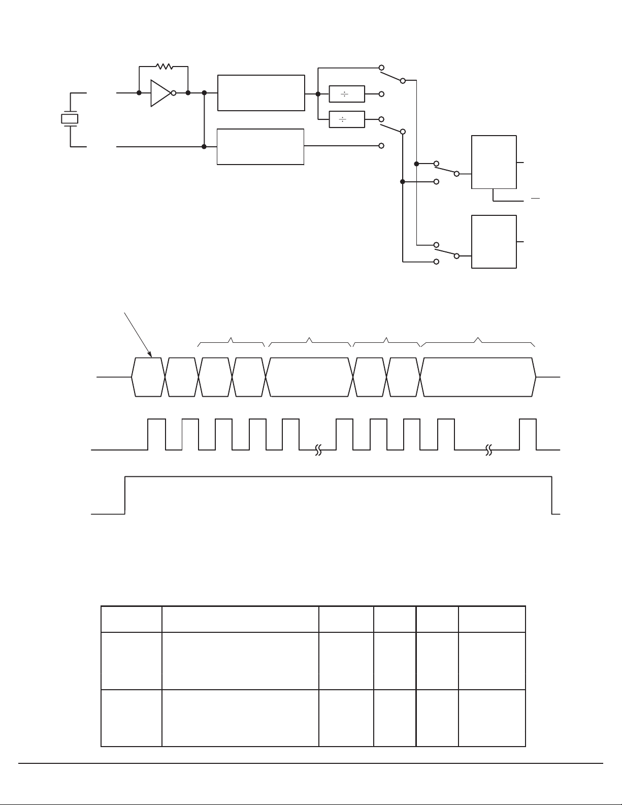
Figure 16 shows the bit function of the reference frequency
programming word. The user can either select the “fixed” reference frequency for all channels accordingly or provide a specific reference frequency for a particular channel by using two
reference frequency counters (e.g., for an application in
France, the base set transmit channel common fixed reference
frequency is 6.25 kHz or 12.5 kHz). (See Table 3 and Figure 6
for reference frequencies for various countries.) However,
transmit channels 6, 8, and 14 can be set to 25 kHz, and channel 8 reference frequency can be set to 50 kHz. But this reference frequency may not be applied to the receiving side; therefore, the receiving side reference frequency must be generated
by another reference frequency counter. The higher the reference frequency, the better the phase noise performance and
faster the lock time, but the PLL consumes more current if
both reference frequency counters are in operation.
In general, the 12–bit reference frequency counter plus the ÷ 4
and ÷ 25 module can offer all the reference frequencies for
global CT–1 transmit and receive channel requirements. Users
can select their own reference frequency by introducing the
additional 14–bit auxiliary reference frequency counter.
Again, the 14–bit auxiliary reference frequency counter can
be shut down by the auxiliary reference enable bit in the reference counter programming word by setting the bit to 0. At this
state, the fR2is automatically connected to point C (the ÷25
block output), and fR1can be connected to point A or B by
setting the fR1–S1 and fR1–S2 bits in the reference counter
program word. The 14–bit auxiliary reference frequency counter data will be in “Don’t Care” state.
If the 14–bit auxiliary reference frequency counter is enabled
(auxiliary reference enable = 1), then fR2is automatically connected to point D (14–bit counter output), and fR1can be
selected to connect to point A, B, or C, depending on the bit
setting of fR1–S1 and fR1–S2. Table 4 and Figure 16 describe
the functions of the auxiliary reference enable bit and the
fR1–S1 and fR1–S2 bits selection.
LANSDALE Semiconductor, Inc.
ML145162
AD
in
D
in
CLK
ENB
NOTE: ENB must be low during the serial transfer.
Figure 15. Programming Format for Transmit and Receive Counters
Table 3. Global CT–1 Reference Frequency Setting vs Channel Frequencies
Country Channels Frequency f
U.S.A. 46/49 MHz (10, 15, 25 Channels) 5.0 kHz —
France 26/41 MHz 6.25 kHz/12.5 kHz —
Spain 31/41 MHz 5.0 kHz —
Australia 30/39 MHz 5.0 kHz —
U.K. 1.7/47 MHz 6.25 kHz 1.0 kHz
New Zealand 1.7/34/40 MHz 6.25 kHz 1.0 kHz
16–BIT Tx COUNTER
DIVDE RATIO
16–BIT Rx COUNTER
DIVIDE RATIO
CLOCK
(4–Pin Interfacing Scheme)
LAST
R1
f
R2
Page 12
www.lansdale.comPage 12 of 24 Issue 0
LANSDALE Semiconductor, Inc.
ML145162
OSC
in
OSC
out
MAXIMUM
CRYSTAL FREQUENCY
16.0 MHz
12–BIT PROGRAMMABLE
REFERENCE COUNTER
14–BIT PROGRAMMABLE
AUXILIARY REFERENCE
COUNTER
25
A
f
R1
B
4
C
f
R2
D
1
0
SELECT
Tx–0
Tx
PHASE
DETECTOR
TxPD
LD
out
REF FREQUENCY
COUNTER IDENTIFIER = 0
D
in
CLK
ENB
0
AUX
REF
ENABLE
REFERENCE
FREQUENCY
SELECT
Tx–0
SELECT
SELECT
Rx–0
REFERENCE
FREQUENCY
COUNTER
12–BITS REF FREQ
DATA
REFERENCE
FREQUENCY
SELECT
f
S1
R1
f
R1
S2
1
Rx–0
0
SELECT
AUXILIARY REFERENCE
FREQUENCY COUNTER
14–BITS AUX REF FREQ
Rx
PHASE
DETECTOR
DATA
RxPD
out
NOTE: ENB must be high during the serial transfer.
Figure 16. Reference Frequency Counter/Selection Programming Mode
Table 4. Bit Function and the Reference Frequency Selection Bit Setting of the
Reference Frequency Counter Programming Word
AUX REF
Enable
0 14–Bit Auxiliary Reference Frequency
1 14–Bit Auxiliary Reference Frequency
N/A = Not Applicable
Auxiliary Reference Frequency
Counter Mode
Counter Disable
Counter Enable
Module
Select
fR2→ C 0
fR2→ D 0
f
R1
S1
0
1 0 fR1→ B
1 1 N/A
0
1 0 fR1→ B
1 1 fR1→ C
f
R1
S2
0
1
0
1
fR1 Routing
N/A
fR1→ A
N/A
fR1→ A
Page 13
www.lansdale.comPage 13 of 24 Issue 0
POWER SAVING OPERATION
This PLL has a programmable power–saving scheme. The
transmit and receive counters and the reference frequency
counter can be powered down individually by setting the TxPD
enable, RxPD enable, and Ref PD enable bits of the control
register. The functions of the power down control bits are
explained in Table 2 and the programming format is in Figure 8.
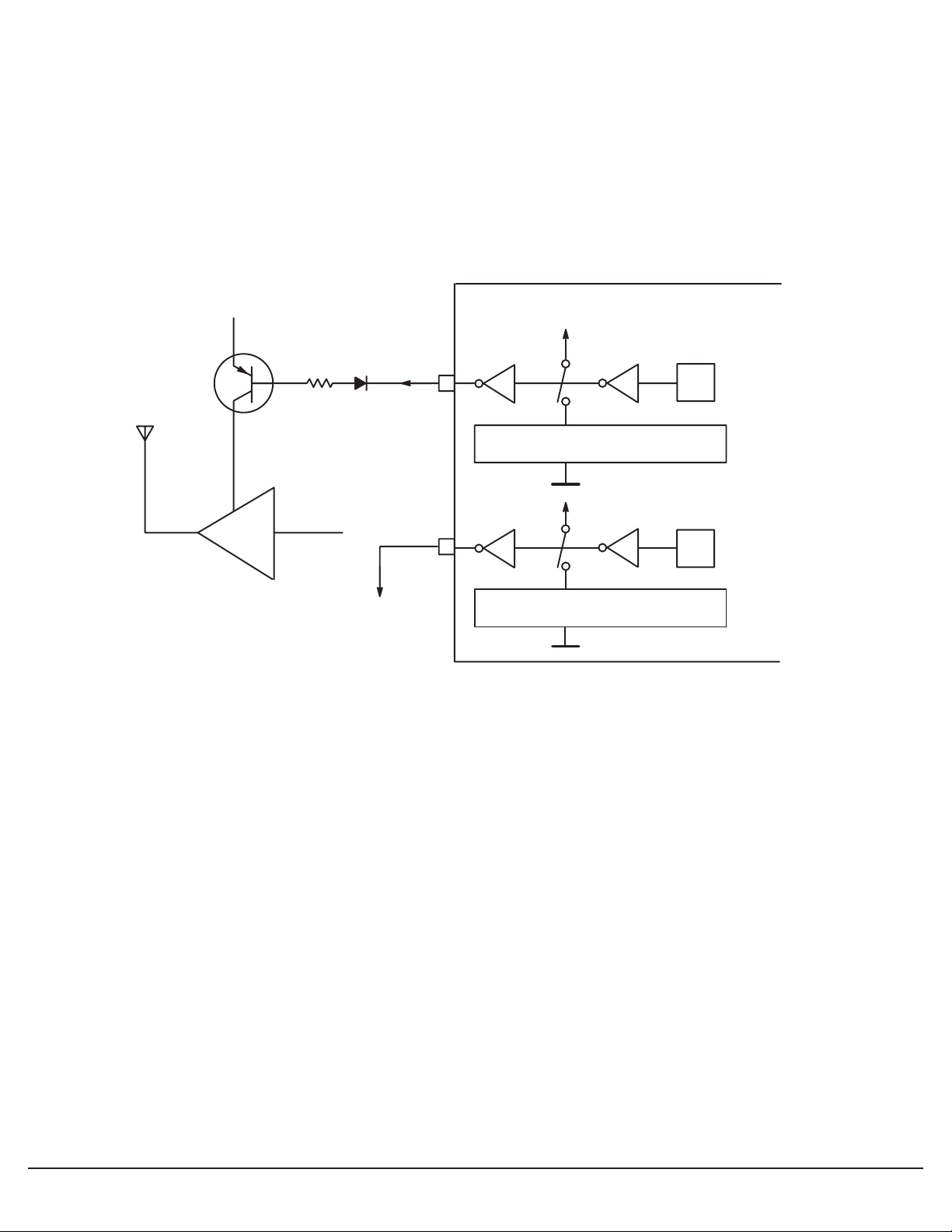
The output pins TxPS/fTxand RxPS/fRxoutput the status of
the internal power saving setting. If the bit TxPD enable is set
“high” (transmit counter is set to power–down mode), then the
TxPS/fTxpin will also output a “high” state. This TxPS/f
Tx
out-put can control an external power switch to switch off the
transmitter, as shown in Figure 17. This scheme can be applied
to the RxPS/fRxoutput to control the receiver power saving
operation as required.
LANSDALE Semiconductor, Inc.
ML145162
POWER SUPPLY
TxPS/f
Tx
POWER SWITCH FOR TRANSMITTER
Tx
POWER
AMP
RxPS/f
Rx
UNIVERSAL DUAL PLL
V
DD
Tx POWER–DOWN
Q
ENABLE FLAG
Tx DIVIDER CHAIN COUNTER, PHASE DETECTOR
V
DD
Rx POWER–DOWN
Q
ENABLE FLAG
TO CONTROL THE RECEIVER
POWER SWITCH
Figure 17. TxPS/fTx and RxPS/fRx Outputs to Control Power Switches
of the Transmitter and the Receiver
Rx DIVIDER CHAIN COUNTER, PHASE DETECTOR
Page 14
www.lansdale.comPage 14 of 24 Issue 0
LANSDALE Semiconductor, Inc.
ML145162
Tx/Rx CHANNEL COUNTER TEST
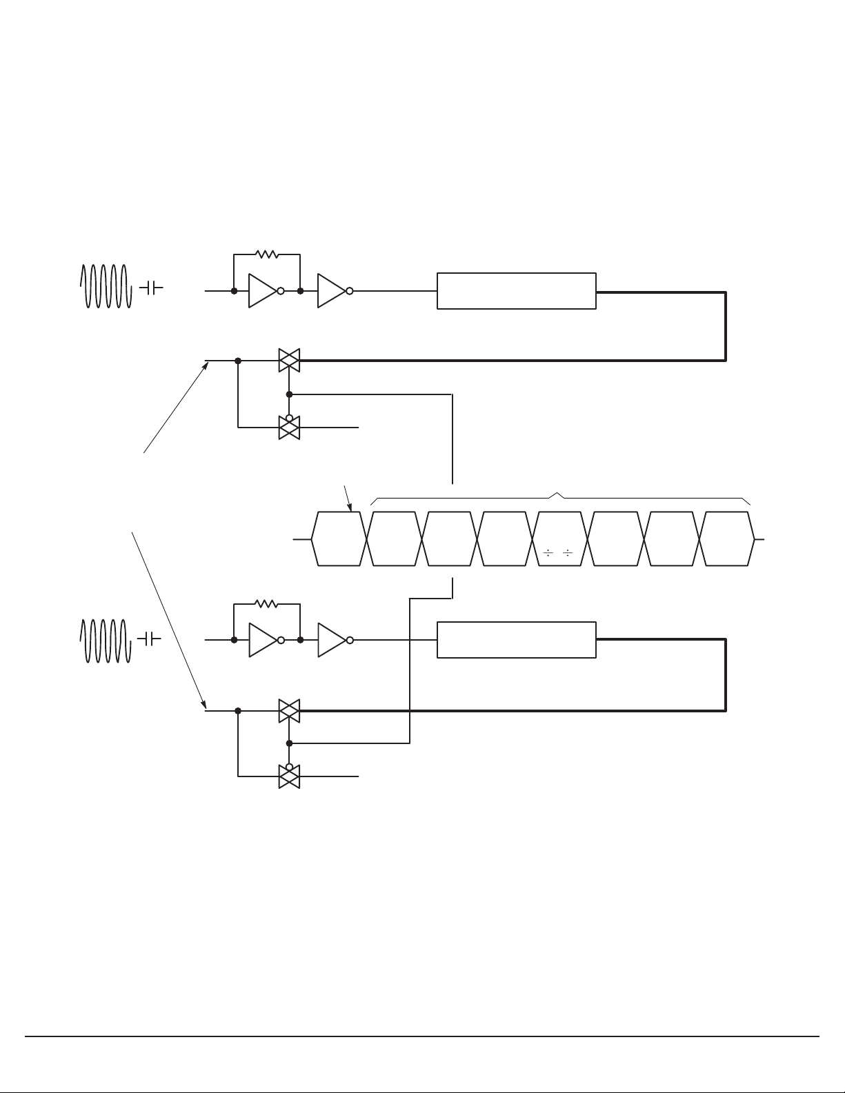
In normal applications, the TxPS/fTxand the RxPS/fRxoutput pins indicate the power saving mode status. However, the
user can examine the Tx and Rx channel counter outputs by
setting the Test bit in the control register to 1. The final value
of the transmit–channel counter and the receive–channel counter multiplex out to TxPS/fTxand RxPS/fRxrespectively. The
user can verify the divided–down output waveform associated
with the RF input level in the PLL circuitry implementation
(Figure 18).
fin–T
f
TxPS / f
Tx
IF TEST BIT IS SET TO 1, THE f
AND fRx ARE MUXED OUT AT PINS
TxPS/fTx AND RxPS/fRx,
RESPECTIVELY, FOR Rx/Tx
CHANNEL COUNTER TEST.
Tx
CONTROL REGISTER IDENTIFIER = 1
D
in
Tx
TxPS
10
16–BIT Tx PROGRAMMABLE
CHANNELS COUNTER
CONTROL REGISTER
TEST
BIT
AUX
DATA
SELECT
REF
OUT
3/ 4
TxPD
ENABLE
RxPD
ENABLE
REF PD
ENABLE
RxPS / f
fin–R
Rx
16–BIT Rx PROGRAMMABLE
CHANNELS COUNTER
f
Rx
RxPS
Figure 18. RF Buffer Sensitivity
Page 15
www.lansdale.comPage 15 of 24 Issue 0
LANSDALE Semiconductor, Inc.
ML145162
Table 5. France CT–1 Base Set Frequency
Channel
Number
1 26.4875 4238 30.7875 4926
2 26.4750 4236 30.7750 4924
3 26.4625 4234 30.7625 4922
4 26.4500 4232 30.7500 4920
5 26.4375 4230 30.7375 4918
6 26.4250 4228 30.7250 4916
7 26.4125 4226 30.7125 4914
8 26.4000 4224 30.7000 4912
9 26.3875 4222 30.6875 4910
10 26.3750 4220 30.6750 4908
11 26.3625 4218 30.6625 4906
12 26.3500 4216 30.6500 4904
13 26.3375 4214 30.6375 4902
14 26.3250 4212 30.6250 4900
15 26.3125 4210 30.6125 4898
Tx Channel
Frequency
(MHz)
Tx Counter Value
(Ref. Freq. =
6.25 kHz)
fin–R Input
Frequency (MHz)
[1st IF = 10.7 MHz]
Rx Counter Value
(Ref. Freq. =
6.25 kHz)
Table 6. France CT–1 Handset Frequency
Channel
Number
1 41.4875 6638 37.1875 5950
2 41.4750 6636 37.1750 5948
3 41.4625 6634 37.1625 5946
4 41.4500 6632 37.1500 5944
5 41.4375 6630 37.1375 5942
6 41.4250 6628 37.1250 5940
7 41.4125 6626 37.1125 5938
8 41.4000 6624 37.1000 5936
9 41.3875 6622 37.0875 5934
10 41.3750 6620 37.0750 5932
11 41.3625 6618 37.0625 5930
12 41.3500 6616 37.0500 5928
13 41.3375 6614 37.0375 5926
14 41.3250 6612 37.0250 5924
15 41.3125 6610 37.0125 5922
Tx Channel
Frequency
(MHz)
Tx Counter Value
(Ref. Freq. =
6.25 kHz)
fin–R Input
Frequency (MHz)
[1st IF = 10.7 MHz]
Rx Counter Value
(Ref. Freq. =
6.25 kHz)
Page 16
www.lansdale.comPage 16 of 24 Issue 0
LANSDALE Semiconductor, Inc.
ML145162
Table 7. Spain CT–1 Base Set Frequency
Channel
Number
1 31.0250 6205 29.2300 5846
2 31.0500 6210 29.2550 5851
3 31.0750 6215 29.2800 5856
4 31.1000 6220 29.3050 5861
5 31.1250 6225 29.3300 5866
6 31.1500 6230 29.3550 5871
7 31.1750 6235 29.3800 5876
8 31.2000 6240 29.4050 5881
9 31.2500 6250 29.4550 5891
10 31.2750 6255 29.4800 5896
11 31.3000 6260 29.5050 5901
12 31.3250 6265 29.5300 5906
Tx Channel
Frequency
(MHz)
Tx Counter Value
(Ref. Freq. =
5.00 kHz)
fin–R Input
Frequency (MHz)
[1st IF = 10.695 MHz]
Rx Counter Value
(Ref. Freq. =
5.00 kHz)
Table 8. Spain CT–1 Handset Frequency
Channel
Number
1 39.9250 7985 20.3300 4066
2 39.9500 7990 20.3550 4071
3 39.9750 7995 20.3800 4076
4 40.0000 8000 20.4050 4081
5 40.0250 8005 20.4300 4086
6 40.0500 8010 20.4550 4091
7 40.0750 8015 20.4800 4096
8 40.1000 8020 20.5050 4101
9 40.1500 8030 20.5550 4111
10 40.1750 8035 20.5800 4116
11 40.2000 8040 20.6050 4121
12 40.2250 8045 20.6300 4126
Tx Channel
Frequency
(MHz)
Tx Counter Value
(Ref. Freq. =
5.00 kHz)
fin–R Input
Frequency (MHz)
[1st IF = 10.7 MHz]
Rx Counter Value
(Ref. Freq. =
5.00 kHz)
Page 17
www.lansdale.comPage 17 of 24 Issue 0
LANSDALE Semiconductor, Inc.
ML145162
Table 9. New Zealand CT–1 Base Set Frequency
Channel
Number
1 1.7820 1782 29.7625 4762
2 1.7620 1762 29.7500 4760
3 1.7420 1742 29.7375 4758
4 1.7220 1722 29.7250 4756
5 1.7020 1702 29.7125 4754
6 34.3500 5496 29.7000 4752
7 34.3625 5498 29.6875 4750
8 34.3750 5500 29.6750 4748
9 34.3875 5502 29.6625 4746
10 34.4000 5504 29.6500 4744
Tx Channel
Frequency
(MHz)
Tx Counter Value
Ref Freq
= 1.0 kHz
Ref Freq
= 6.25 kHz
fin–R Input
Frequency (MHz)
[1st IF = 10.7 MHz]
Rx Counter Value
(Ref. Freq. =
Table 10. New Zealand CT–1 Handset Frequency
Channel
Number
1 40.4625 6474 2.2370 2237
2 40.4500 6472 2.2170 2217
3 40.4375 6470 2.1970 2197
4 40.4250 6468 2.1770 2177
5 40.4125 6466 2.1570 2157
6 40.4000 6464 23.6500 3784
7 40.3875 6462 23.6625 3786
8 40.3750 6460 23.6750 3788
9 40.3625 6458 23.6875 3790
10 40.3500 6456 23.7000 3792
Tx Channel
Frequency
(MHz)
Tx Counter Value
(Ref. Freq. =
6.25 kHz)
fin–R Input
Frequency (MHz)
Ref Freq
= 455 kHz
Ref Freq
= 10.7 kHz
Rx Counter Value
6.25 kHz)
Ref Freq
= 1.0 kHz
Ref Freq
= 6.25 kHz
Page 18
www.lansdale.comPage 18 of 24 Issue 0
LANSDALE Semiconductor, Inc.
ML145162
Table 11. Australia CT–1 Base Set Frequency
Channel
Number
1 30.0750 6015 29.0800 5816
2 30.1250 6025 29.1300 5826
3 30.1750 6035 29.1800 5836
4 30.2250 6045 29.2300 5846
5 30.2750 6055 29.2800 5856
6 30.1000 6020 29.1050 5821
7 30.1500 6030 29.1550 5831
8 30.2000 6040 29.2050 5841
9 30.2500 6050 29.2550 5851
10 30.3000 6060 29.3050 5861
Tx Channel
Frequency
(MHz)
Tx Counter Value
(Ref. Freq. =
5.00 kHz)
fin–R Input
Frequency (MHz)
[1st IF = 10.695 MHz]
Rx Counter Value
(Ref. Freq. =
Table 12. Australia CT–1 Handset Frequency
Channel
Number
1 39.7750 7955 19.3800 3876
2 39.8250 7965 19.4300 3886
3 39.8750 7975 19.4800 3896
4 39.9250 7985 19.5300 3906
5 39.9750 7995 19.5800 3916
6 39.8000 7960 19.4050 3881
7 39.8500 7970 19.4550 3891
8 39.9000 7980 19.5050 3901
9 39.9500 7990 19.5550 3911
10 40.0000 8000 19.6050 3921
Tx Channel
Frequency
(MHz)
Tx Counter Value
(Ref. Freq. =
5.00 kHz)
fin–R Input
Frequency (MHz)
[1st IF = 10.7 MHz]
Rx Counter Value
(Ref. Freq. =
5.00 kHz)
5.00 kHz)
Page 19
www.lansdale.comPage 19 of 24 Issue 0
LANSDALE Semiconductor, Inc.
ML145162
Table 13. U.K. CT–1 Base Set Frequency
Channel
Number
1 1.6420 1642 36.75625 5881
2 1.6620 1662 36.76875 5883
3 1.6820 1682 36.78125 5885
4 1.7020 1702 36.79375 5887
5 1.7220 1722 36.80625 5889
6 1.7420 1742 36.81875 5891
7 1.7620 1762 36.83125 5893
8 1.7820 1782 36.84375 5895
Tx Channel
Frequency
(MHz)
Tx Counter Value
(Ref. Freq. =
1.00 kHz)
fin–R Input
Frequency (MHz)
[1st IF = 10.7 MHz]
Rx Counter Value
Table 14. U.K. CT–1 Handset Frequency
Channel
Number
1 47.45625 7593 2.097 2097
2 47.46875 7595 2.117 2117
3 47.48125 7597 2.137 2137
4 47.49375 7599 2.157 2157
5 47.50625 7601 2.177 2177
6 47.51875 7603 2.197 2197
7 47.53125 7605 2.217 2217
8 47.54375 7607 2.237 2237
Tx Channel
Frequency
(MHz)
Tx Counter Value
(Ref. Freq. =
6.25 kHz)
fin–R Input
Frequency (MHz)
[1st IF = 455 kHz]
Rx Counter Value
(Ref. Freq. =
6.25 kHz)
(Ref. Freq. =
1.00 kHz)
Page 20
www.lansdale.comPage 20 of 24 Issue 0
LANSDALE Semiconductor, Inc.
ML145162
Table 15. U.S.A. (10 Channels) CT–1 Base Set Frequency
Channel
Number
1 46.610 9322 38.975 7795
2 46.630 9326 38.150 7830
3 46.670 9334 38.165 7833
4 46.710 9342 39.075 7815
5 46.730 9346 39.180 7836
6 46.770 9354 39.135 7827
7 46.830 9366 39.195 7839
8 46.870 9374 39.235 7847
9 46.930 9386 39.295 7859
10 46.970 9394 39.275 7855
Tx Channel
Frequency
(MHz)
Tx Counter Value
(Ref. Freq. =
5.00 kHz)
fin–R Input
Frequency (MHz)
[1st IF = 10.695 MHz]
Rx Counter Value
(Ref. Freq. =
Table 16. U.S.A. (10 Channels) CT–1 Handset Frequency
Channel
Number
1 49.670 9934 35.915 7183
2 49.845 9969 35.935 7187
3 49.860 9972 35.975 7195
4 49.770 9954 36.015 7203
5 49.875 9975 36.035 7207
6 49.830 9966 36.075 7215
7 49.890 9978 36.135 7227
8 49.930 9986 36.175 7235
9 49.990 9998 36.235 7247
10 49.970 9994 36.275 7255
Tx Channel
Frequency
(MHz)
Tx Counter Value
(Ref. Freq. =
5.00 kHz)
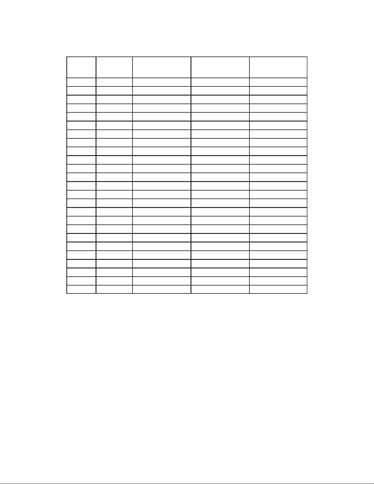
fin–R Input
Frequency (MHz)
[1st IF = 10.7 MHz]
Rx Counter Value
(Ref. Freq. =
5.00 kHz)
5.00 kHz)
Page 21
www.lansdale.comPage 21 of 24 Issue 0
LANSDALE Semiconductor, Inc.
ML145162
Table 17. U.S.A. (25 Channels) CT–1 Base Set Frequency
Channel
Number
1 43.72 8744 38.06 7612
2 43.74 8748 38.14 7628
3 43.82 8764 38.16 7632
4 43.84 8768 38.22 7644
5 43.92 8784 38.32 7664
6 43.96 8788 38.38 7676
7 44.12 8824 38.40 7680
8 44.16 8832 38.46 7692
9 44.18 8836 38.50 7700
10 44.20 8840 38.54 7708
11 44.32 8864 38.58 7716
12 44.36 8872 38.66 7732
13 44.40 8880 38.70 7740
14 44.46 8892 38.76 7752
15 44.48 8896 38.80 7760
16 46.61 9322 38.97 7794
17 46.63 9326 39.145 7829
18 46.67 9334 39.16 7832
19 46.71 9342 39.07 7814
20 46.73 9346 39.175 7835
21 46.77 9354 39.13 7826
22 46.83 9366 39.19 7838
23 46.87 9374 39.23 7846
24 46.93 9386 39.29 7858
25 46.97 9394 39.27 7854
Tx Channel
Frequency
(MHz)
Tx Counter Value
(Ref. Freq. =
5.00 kHz)
fin–R Input
Frequency (MHz)
[1st IF = 10.7 MHz]
Rx Counter Value
(Ref. Freq. =
5.00 kHz)
Page 22
www.lansdale.comPage 22 of 24 Issue 0
LANSDALE Semiconductor, Inc.
ML145162
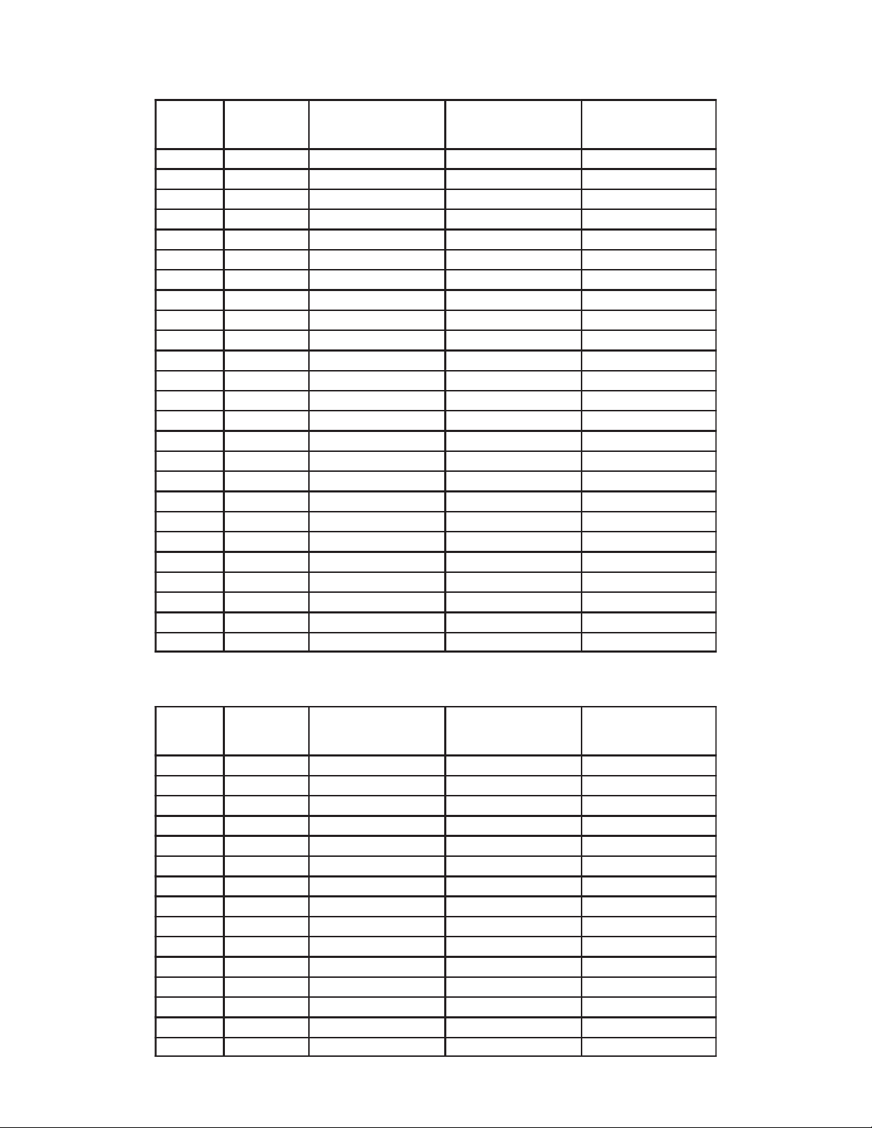
Table 18. U.S.A. (25 Channels) CT–1 Handset Frequency
Channel
Number
1 48.76 9752 33.02 6604
2 48.84 9768 33.04 6608
3 48.86 9772 33.12 6624
4 48.92 9748 33.14 6628
5 49.02 9804 33.22 6644
6 49.08 9816 33.26 6652
7 49.10 9820 33.42 6684
8 49.16 9832 33.46 6692
9 49.20 9840 33.48 6696
10 49.24 9848 33.50 6700
11 49.28 9856 33.62 6724
12 49.36 9872 33.66 6732
13 49.40 9880 33.70 6740
14 49.46 9892 33.76 6752
15 49.50 9900 33.78 6756
16 49.67 9934 33.91 7182
17 49.845 9969 33.93 7186
18 49.86 9972 33.97 7194
19 49.77 9954 36.01 7202
20 49.875 9975 36.03 7206
21 49.83 9966 36.07 7214
22 49.89 9978 36.13 7226
23 49.93 9986 36.17 7234
24 49.99 9998 36.23 7246
25 49.97 9994 36.27 7254
Tx Channel
Frequency
(MHz)
Tx Counter Value
(Ref. Freq. =
5.00 kHz)
fin–R Input
Frequency (MHz)
[1st IF = 10.7 MHz]
Rx Counter Value
(Ref. Freq. =
5.00 kHz)
Table 19. Korea CT–1 Base Set Frequency
Channel
Number
1 46.610 9322 38.975 7795
2 46.630 9326 38.150 7830
3 46.670 9334 38.165 7833
4 46.710 9342 39.075 7815
5 46.730 9346 39.180 7836
6 46.770 9354 39.135 7827
7 46.830 9366 39.195 7839
8 46.870 9374 39.235 7847
9 46.930 9386 39.295 7859
10 46.970 9394 39.275 7855
11 46.510 9302 39.000 7800
12 46.530 9306 39.015 7803
13 46.550 9310 39.030 7806
14 46.570 9314 39.045 7809
15 46.590 9318 39.060 7812
Tx Channel
Frequency
(MHz)
Tx Counter Value
(Ref. Freq. =
5.00 kHz)
fin–R Input
Frequency (MHz)
[1st IF = 10.695 MHz]
Rx Counter Value
(Ref. Freq. =
5.00 kHz)
Page 23
www.lansdale.comPage 23 of 24 Issue 0
LANSDALE Semiconductor, Inc.
ML145162
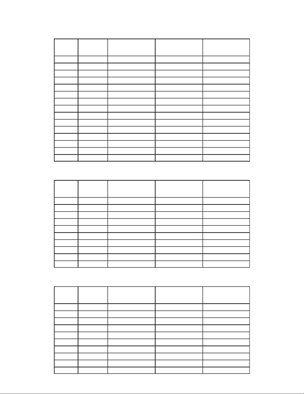
Table 20. Korea CT–1 Handset Frequency
Channel
Number
1 49.670 9934 35.915 7183
2 49.845 9969 35.935 7187
3 49.860 9972 35.975 7195
4 49.770 9954 36.015 7203
5 49.875 9975 36.035 7207
6 49.830 9966 36.075 7215
7 49.890 9978 36.135 7227
8 49.930 9986 36.175 7235
9 49.990 9998 36.235 7247
10 49.970 9994 36.275 7255
11 49.695 9939 35.815 7163
12 49.710 9942 35.835 7167
13 49.725 9945 35.855 7171
14 49.740 9948 35.875 7175
15 49.755 9951 35.895 7179
Tx Channel
Frequency
(MHz)
Tx Counter Value
(Ref. Freq. =
5.00 kHz)
fin–R Input
Frequency (MHz)
[1st IF = 10.7 MHz]
Rx Counter Value
(Ref. Freq. =
5.00 kHz)
Table 21. China CT–1 Base Set Frequency
Channel
Number
1 45.250 9050 37.550 7510
2 45.275 9055 37.575 7515
3 45.300 9060 37.600 7520
4 45.325 9065 37.625 7525
5 45.350 9070 37.650 7530
6 45.375 9075 37.675 7535
7 45.400 9080 37.700 7540
8 45.425 9085 37.725 7545
9 45.450 9090 37.750 7550
10 45.475 9095 37.775 7555
Tx Channel
Frequency
(MHz)
Tx Counter Value
(Ref. Freq. =
5.00 kHz)
fin–R Input
Frequency (MHz)
[1st IF = 10.7 MHz]
Rx Counter Value
(Ref. Freq. =
Table 22. China CT–1 Handset Frequency
Channel
Number
1 48.250 9650 34.550 6910
2 48.275 9655 34.575 6915
3 48.300 9660 34.600 6920
4 48.325 9665 34.625 6925
5 48.350 9670 34.650 6930
6 48.375 9675 34.675 6935
7 48.400 9680 34.700 6940
8 48.425 9685 34.725 6945
9 48.450 9690 34.750 6950
10 48.475 9695 34.775 6955
Tx Channel
Frequency
(MHz)
Tx Counter Value
(Ref. Freq. =
5.00 kHz)
fin–R Input
Frequency (MHz)
[1st IF = 10.7 MHz]
Rx Counter Value
(Ref. Freq. =
5.00 kHz)
5.00 kHz)
Page 24
www.lansdale.comPage 24 of 24 Issue 0
LANSDALE Semiconductor, Inc.
ML145162
Lansdale Semiconductor reserves the right to make changes without further notice to any products herein to improve reliability, function or design. Lansdale does not assume any liability arising out of the application or use of any product or circuit
described herein; neither does it convey any license under its patent rights nor the rights of others. “Typical” parameters which
may be provided in Lansdale data sheets and/or specifications can vary in different applications, and actual performance may
vary over time. All operating parameters, including “Typicals” must be validated for each customer application by the customer’s
technical experts. Lansdale Semiconductor is a registered trademark of Lansdale Semiconductor, Inc.
–A–
916
B
18
F
C
S
–T–
H
G
D
16 PL
0.25 (0.010) T
K
M
A
–A–
16 9
–B–
18
G
K
C
–T–
SEATING
PLANE
D
16 PL
0.25 (0.010) A
M
S
B
T
S
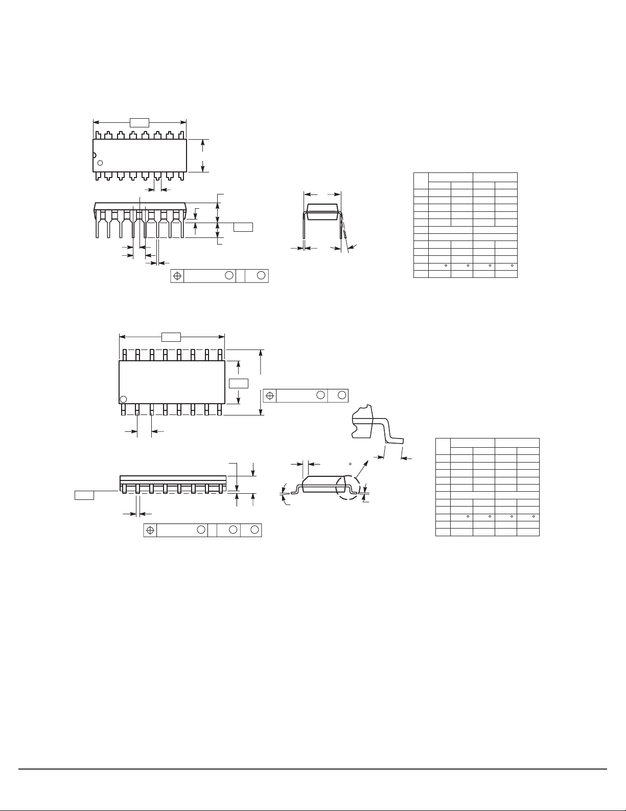
OUTLINE DIMENSIONS
P DIP 16 = EP
(ML145162EP)
PLASTIC DIP
CASE 648–08
L
SEATING
PLANE
J
M
SOG 16 = -5P
(ML145162-5P)
SOG PACKAGE
CASE 751B–05
8 PLP
M
0.25 (0.010) B
M
S
R
X 45
NOTES:
1. DIMENSIONING AND TOLERANCING PER ANSI
Y14.5M, 1982.
2. CONTROLLING DIMENSION: INCH.
3. DIMENSION L TO CENTER OF LEADS WHEN
FORMED PARALLEL.
4. DIMENSION B DOES NOT INCLUDE MOLD FLASH.
5. ROUNDED CORNERS OPTIONAL.
DIM MIN MAX MIN MAX
A 0.740 0.770 18.8019.55
B 0.250 0.270 6.356.85
C 0.145 0.175 3.69 4.44
D 0.015 0.021 0.39 0.53
F 0.040 0.70 1.02 1.77
G 0.100 BSC2.54 BSC
M
J
H 0.050 BSC1.27 BSC
J 0.008 0.015 0.21 0.38
K 0.110 0.1302.80 3.30
L 0.295 0.305 7.50 7.74
M 0 10 0 10
S 0.020 0.040 0.51 1.01
NOTES:
1. DIMENSIONING AND TOLERANCING PER ANSI
Y14.5M, 1982.
2. CONTROLLING DIMENSION: MILLIMETER.
3. DIMENSIONS A AND B DO NOT INCLUDE
MOLD PROTRUSION.
4. MAXIMUM MOLD PROTRUSION 0.15 (0.006)
PER SIDE.
5. DIMENSION D DOES NOT INCLUDE DAMBAR
PROTRUSION. ALLOWABLE DAMBAR
PROTRUSION SHALL BE 0.127 (0.005) TOTAL
IN EXCESS OF THE D DIMENSION AT
MAXIMUM MATERIAL CONDITION.
DIM MIN MAX MIN MAX
F
A 9.80 10.00 0.386 0.393
B 3.80 4.00 0.150 0.157
C 1.35 1.75 0.054 0.068
D 0.35 0.49 0.014 0.019
F 0.40 1.25 0.016 0.049
G 1.27 BSC 0.050 BSC
J 0.19 0.25 0.008 0.009
K 0.10 0.25 0.004 0.009
M 0 7 0 7
P 5.80 6.20 0.229 0.244
R 0.25 0.50 0.010 0.019
MILLIMETERSINCHES
INCHESMILLIMETERS
 Loading...