

Page 1
Legacy Device: Motorola MC1350
The ML1350 is an integrated circuit featuring wide range
AGC for use as a linear IF amplifier in AM radio, shortwave,
TV and instrumentation.
• Power Gain: 50 dB Typ at 45 MHz
50 dB Typ at 58 MHz
• AGC Range: 60 dB Min, DC to 45 MHz
• Nearly Constant Input & Output Admittance over the
Entire AGC Range
•
• Low Reverse Transfer Admittance: << 1.0 µmho Typical
• 12 V Operation, Single–Polarity Power Supply
• Operating Temperature Range TA= 0° to +75° C
Note: See ML1490 Similar Function
Constant (–3.0 dB) to 90 MHz
Y21
MAXIMUM RATINGS
Power Supply Voltage V
Output Supply Voltage V1, V
AGC Supply Voltage V
Differential Input Voltage V
Power Dissipation (Package Limitation)
Plastic Package
Derate above
Operating Temperature Range T
(TA = +25°C, unless otherwise noted.)
Rating
25°C
Symbol Value Unit
+
AGC
in
P
D
A
8
0 to +75 °C
+18 Vdc
+18 Vdc
+
V
5.0 Vdc
625
5.0
ML1350
Monolithic IF Amplifier
P DIP = PP
8
1
SO 8 = -5P
PLASTIC PACKAGE
CASE 751
(SO–8)
CROSS REFERENCE/ORDERING INFORMATION
P DIP 8 MC1350P ML1350PP
SO 8 MC1350D ML1350-5P
Note: Lansdale lead free (Pb) product, as it
becomes available, will be identified by a part
number prefix change from ML to MLE.
Vdc
mW
mW/°C
PLASTIC PACKAGE
CASE 626
8
MOTOROLA
1
LANSDALEPACKAGE
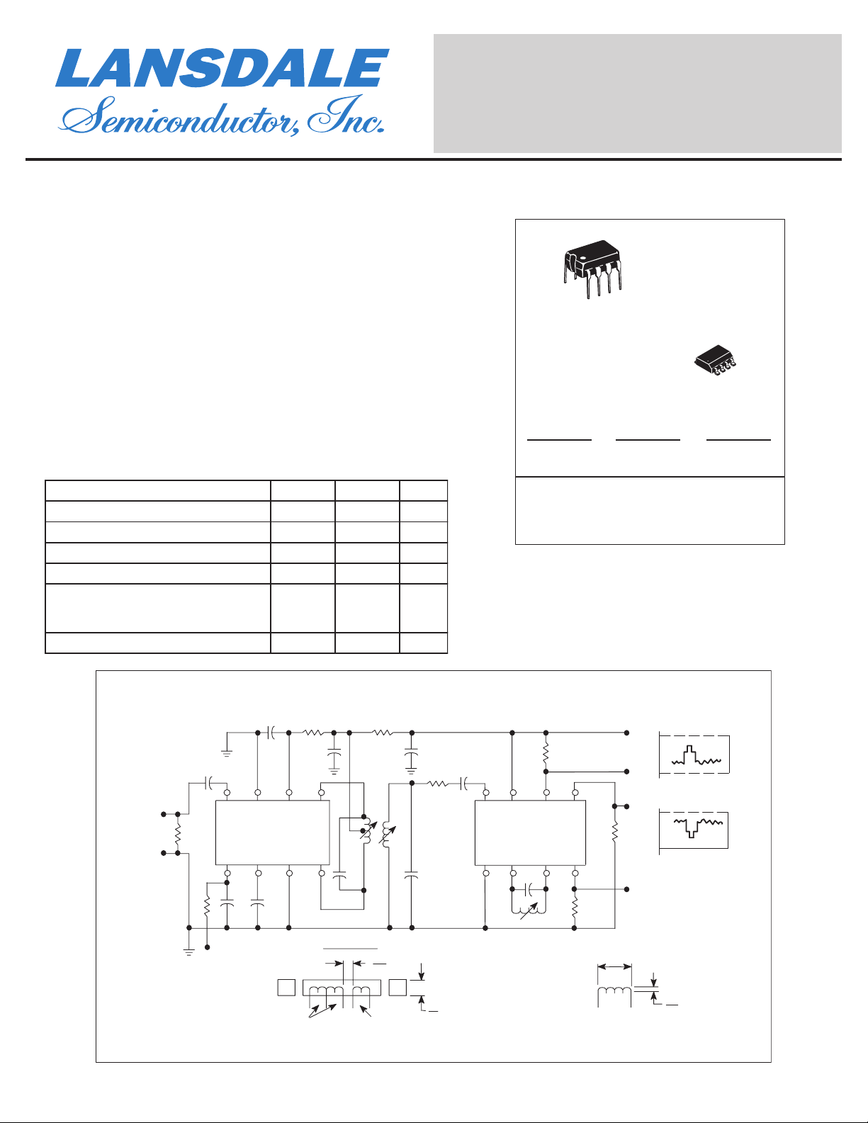
Figure 1. Typical ML1350 Video IF Amplifier and MC1330 Low–Level Video Detector Circuit
45MHz
Input
0.001µF
4
50
567
5.0k
AGC
0.002µF
ML1350
F
µ
0.002
470 220
µ
F
0.002
32 1
T1
8
F
µ
0.002
5
Turns
All windings #30 AWG tinned nylon acetate
wire tuned with Carbonyl E or J slugs.
T1
20pF
5
≈
16
Turns
0.1
12pF
"
6
+18Vdc
µ
F
68pF
22
1
"
4
76 5 4
83 2 1
3.3k
MC1330AP
33pF
L1
Auxiliary Video
Output
3.9k
3
16
10
Turns
L1 wound with #26 AWG tinned nylon
acetate wire tuned by distorting winding.
www.lansdale.comPage 1 of 6 Issue A
18V
10V
Primary Video
and Sound Output
7.7V
3.9k
0
AFT Output
"
3
16
"
Page 2
ML1350
LANSDALE Semiconductor, Inc.
ELECTRICAL CHARACTERISTICS
Characteristics
AGC Range, 45 MHz (5.0 V to 7.0 V) (Figure 1) 60 68 – dB
Power Gain (Pin 5 grounded via a 5.1 kΩ resistor)
f = 58 MHz, BW = 4.5 MHz See Figure 6(a)
f = 45 MHz, BW = 4.5 MHz See Figure 6(a), (b)
f = 10.7 MHz, BW = 350 kHz See Figure 7
f = 455 kHz, BW = 20 kHz
Maximum Differential Voltage Swing
0 dB AGC
–30 dB AGC
Output Stage Current (Pins 1 and 8) I1 + I
Total Supply Current (Pins 1, 2 and 8) I
Power Dissipation P
DESIGN PARAMETERS, Typical Values (V
Parameter Symbol 455 kHz 10.7 MHz 45 MHz 58 MHz Unit
Single–Ended Input Admittance g
Input Admittance Variations with AGC
(0 dB to 60 dB)
Differential Output Admittance g
Output Admittance Variations with AGC
(0 dB to 60 dB)
Reverse Transfer Admittance (Magnitude) |y12| < < 1.0 < < 1.0 < < 1.0 < < 1.0 µmho
Forward Transfer Admittance
Magnitude
Angle (0 dB AGC)
Angle (–30 dB AGC)
Single–Ended Input Capacitance C
Differential Output Capacitance C
(V+ = +12 Vdc, TA = +25°C, unless otherwise noted.)
Symbol Min Typ Max Unit
A
p
V
O
8
S
D
+
= +12 Vdc, TA = +25°C, unless otherwise noted.)
11
b
11
∆g
∆b
22
b
22
∆g
∆b
|y21|
< y
< y
11
11
22
22
21
21
in
O
0.31
0.022
–
–
4.0
3.0
–
–
160
–5.0
–3.0
7.2 7.2 7.4 7.6 pF
1.2 1.2 1.3 1.6 pF
–
46
–
–
–
–
– 5.6 – mA
– 14 17 mAdc
– 168 204 mW
Frequency
0.36
0.50
–
–
4.4
110
–
–
160
–20
–18
0.39
2.30
60
0
30
390
4.0
90
200
–80
–69
48
50
58
62
20
8.0
–
–
–
–
–
–
0.5
2.75
–
–
60
510
–
–
180
–105
–90
mmho
µmho
µmho
µmho
mmho
Degrees
Degrees
dB
V
pp
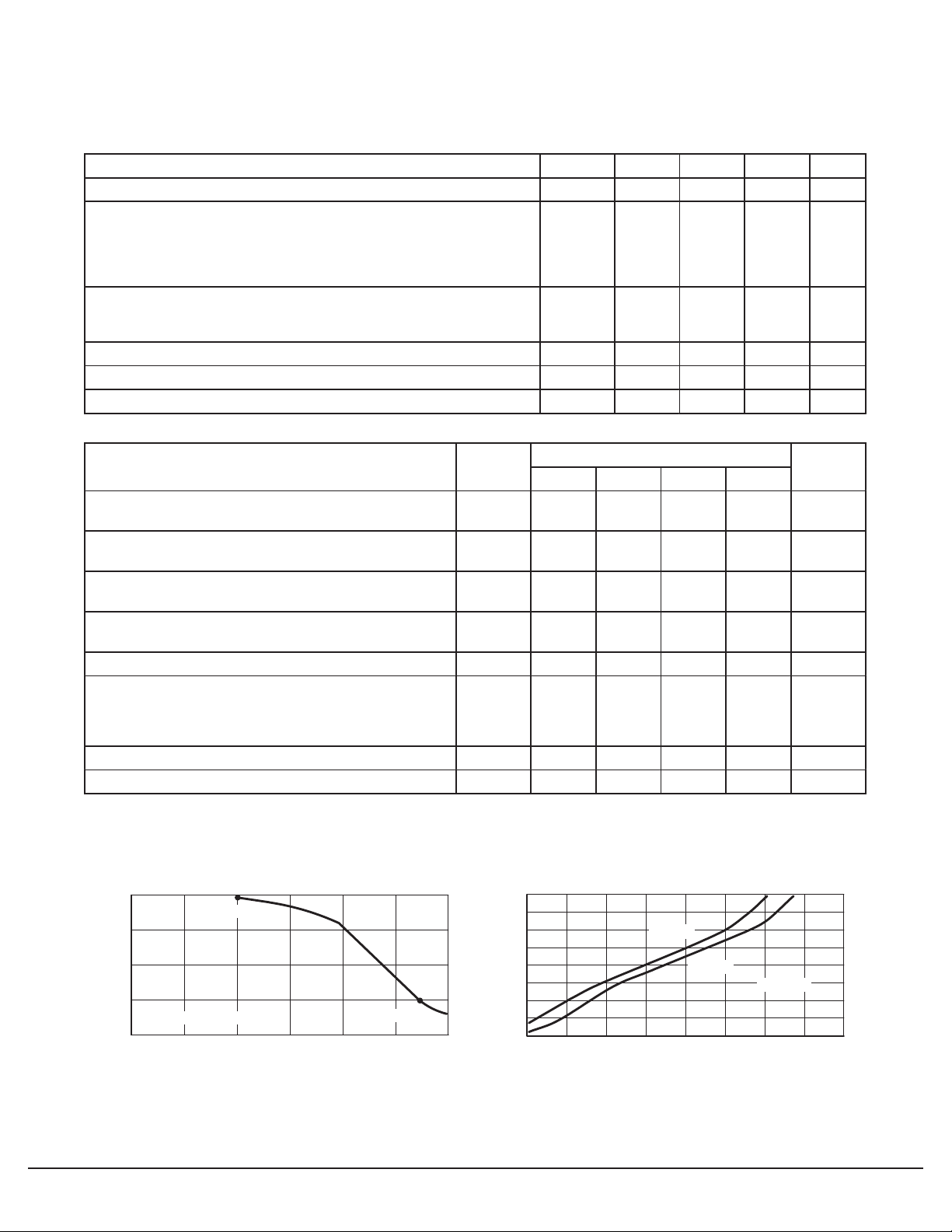
Figure 2. Typical Gain Reduction Figure 3. Noise Figure versus Gain Reduction
0
I
= 0.1 mA
20
40
60
GAIN REDUCTION (dB)
80
4.0 5.0 6.0 7.0
AGC
(Figures 6 and 7)
V
, SUPPLY VOLTAGE (V)
AGC
I
AGC
= 0.2 mA
22
20
18
16
14
12
10
NOISE FIGURE (dB)
8.0
6.0
0 10203040
58 MHz
45 MHz
(Figure 6)
GAIN REDUCTION (dB)
www.lansdale.comPage 2 of 6 Issue A
Page 3
ML1350
LANSDALE Semiconductor, Inc.
GENERAL OPERATING INFORMATION
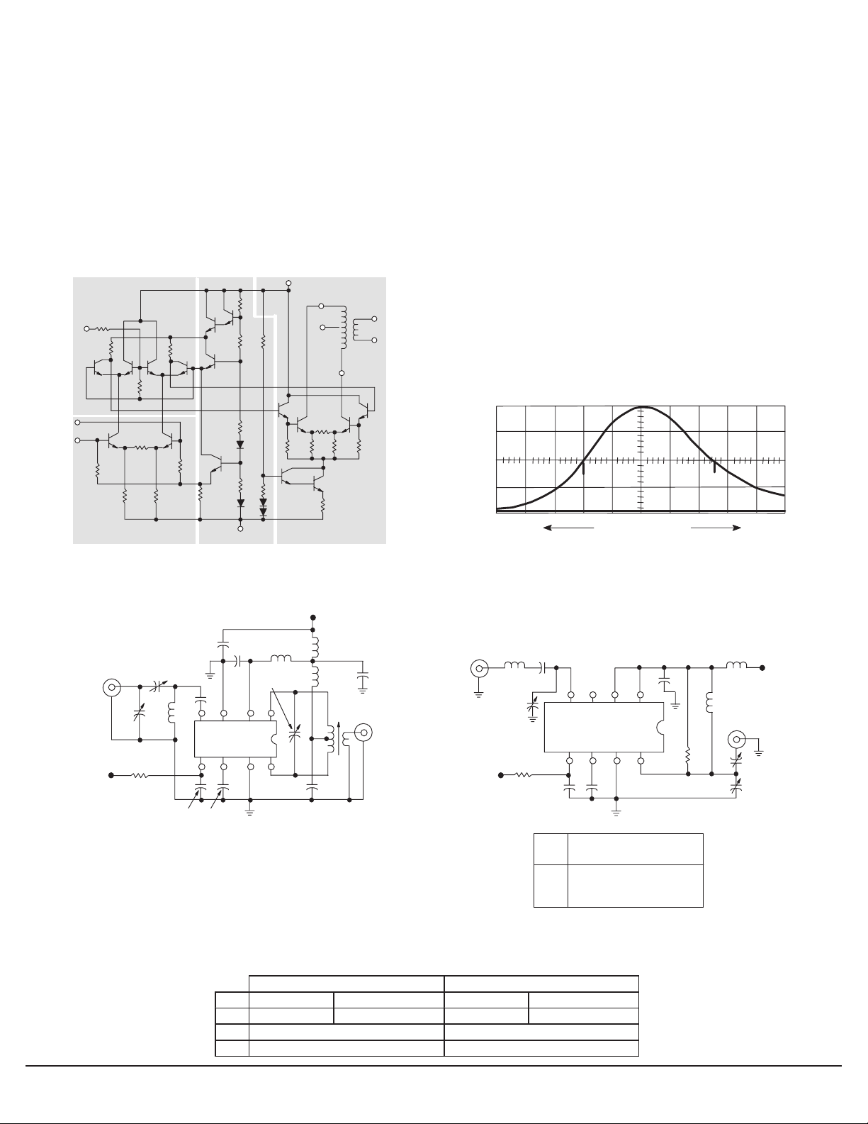
The input amplifiers (Q1 and Q2) operate at constant emitter
currents so that input impedance remains independent of AGC
action. Input signals may be applied single–ended or differentially (for AC) with identical results. Terminals 4 and 6 may be
driven from a transformer, but a DC path from either terminal
to ground is not permitted.
Figure 4. Circuit Schematic
AGC Amplifier Section
AGC
70
Input
5
4 ( – )
6 ( + )
5.0k
470
Inputs
Q1 Q266
1.1k
2.0k
1.1k
5.53k
470
Q6Q5Q3 Q4
1.4k
5.0k
5.6k
8.4k
7
Gnd
Input Amplifier Section Bias Supplies Output Amplifier Section
1.47k
12.1
1.9k
V+
k
Q7
2
(+)
8
V + +
Q845Q9
2.8k 200 200 2.8k
Output
1 ( – )
Q10
200
AGC action occurs as a result of an increasing voltage on the
base of Q4 and Q5 causing these transistors to conduct more
heavily thereby shunting signal current from the interstage
amplifiers Q3 and Q6. The output amplifiers are supplied from
an active current source to maintain constant quiescent bias
thereby holding output admittance nearly constant. Collector
voltage for the output amplifier must be supplied through a
center–tapped tuning coil to Pins 1 and 8. The 12 V supply
(V+) at Pin 2 may be used for this purpose, but output admittance remains more nearly constant if a separate 15 V supply
(V+ +) is used, because the base voltage on the output amplifier varies with AGC bias.
Figure 5. Frequency Response Curve
(45 MHz and 58 MHz)
Scale: 1.0 MHz/cm
Figure 6. Power Gain, AGC and Noise Figure Test Circuits
(a) 45 MHz and 58 MHz
0.001
µ
Input
RS = 50
V
AGC
F
Ω
C2
0.001
µ
F
L1
C1
*
43 21
ML1350
56 785.1k
µ
F0.001µF
0.001
0.001µF
L
1.5–20pF
*Connect to ground for maximum power gain test.
All power supply chokes (Lp), are self–resonant at input frequency. LP
See Figure 5 for Frequency Response Curve.
"
L1 @ 45 MHz = 7 1/4 Turns on a 1/4
L1 @ 58 MHz = 6 Turns on a 1/4
T1 Primary Winding
Secondary Winding
= 18 Turns on a 1/4" coil form, center–tapped, #25 AWG
= 2 Turns centered over Primary Winding @ 45 MHz
coil form
"
coil form
= 1 Turn @ 58 MHz
Slug
= Carbonyl E or J
L1 0.4 µH Q ≥ 100 0.3 µH Q ≥ 100
T1 1.3 µH to 3.4 µH Q ≥ 100 @ 2.0 µH 1.2 µH to 3.8 µH Q ≥ 100 @ 2.0 µH
C1 50 pF to 160 pF 8.0 pF to 60 pF
C2 8.0 pF to 60 pF 3.0 pF to 35 pF
P
0.001
+12V
L
P
L
P
T1
RL = 50
µ
F
45 MHz
Output
(b) Alternate 45 MHz
Input
Ω
≥
20 kΩ.
RS = 50
V
AGC
µ
H .001
0.68
0.1
Ω
C1
5.1k
58 MHz
43 2 1
ML1350
56 7 8
0.001
0.001
L1
C1
C2
C3
14 Turns 28 S.W.G.
5.1k
Ferrite Core
5–25 pF
5–25 pF
5–25 pF
0.33
L1
µ
H
RL = 50
C2
C3
+12V
Ω
Output
www.lansdale.comPage 3 of 6 Issue A
Page 4
ML1350
Legacy Applications Information
LANSDALE Semiconductor, Inc.
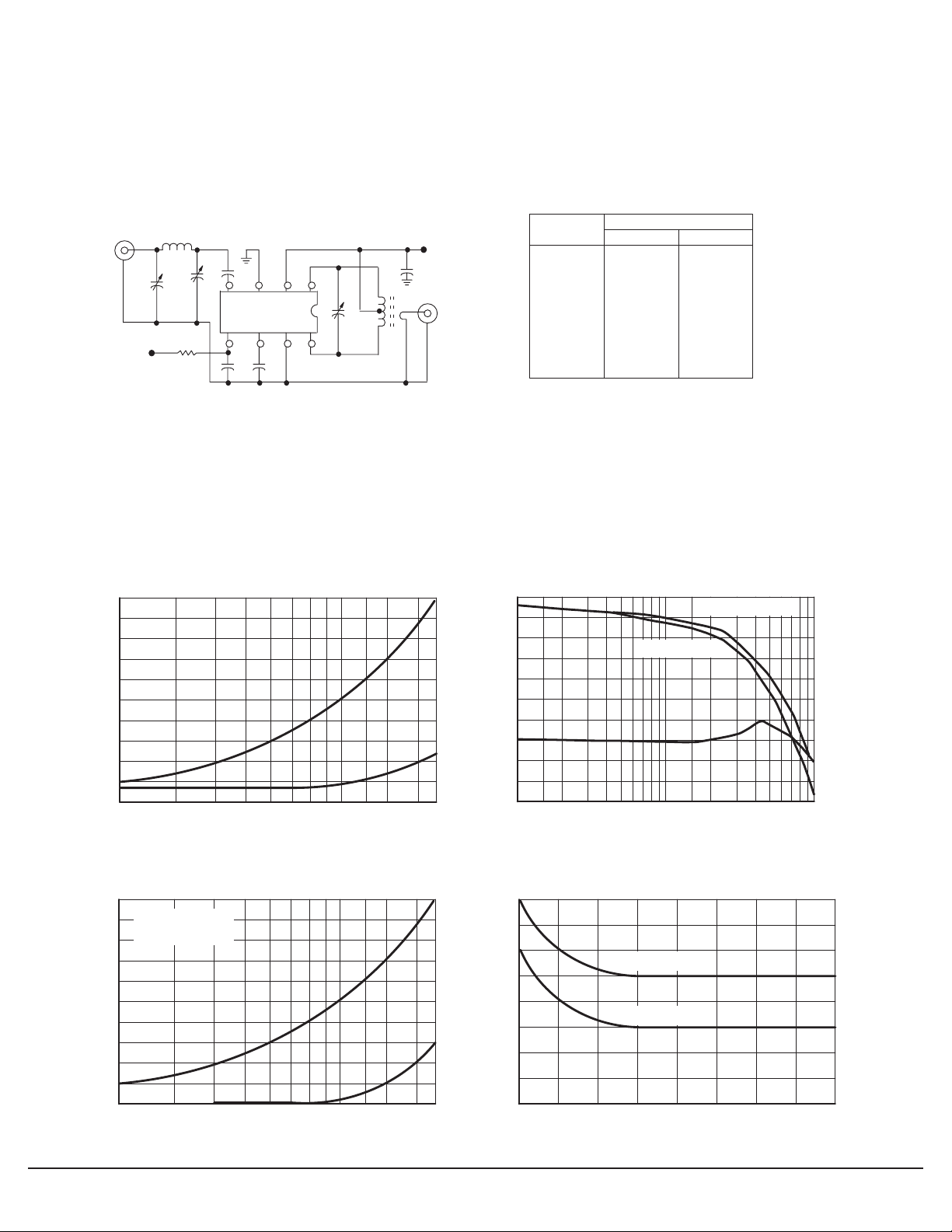
Figure 7. Power Gain and AGC Test Circuit
(455 kHz and 10.7 MHz)
Input
RS = 50
V
AGC
*Grounded for
maximum power gain.
5.0
4.0
3.0
(mmhos),b
2.0
11 11
g
1.0
Ω
L1
C3
C2
C1
*
4321
MC1350
5.1k
5678
C7 C6
C5
12 V
C4
T1
Output
Ω
RS = 50
Component
C1
C2
C3
C4
C5
C8
C7
L1
T1
NOTES: 1. Primary: 120 µH (center–tapped)
NOTES: 1. Qu = 140 at 455 kHz
NOTES: 1. Primary: Secondary turns ratio ≈ 13
NOTES: 2. Primary: 6.0 µH
NOTES: 2. Primary winding = 24 turns #36 AWG
NOTES: 2. (close–wound on 1/4" dia. form)
NOTES: 2. Core = Carbonyl E or J
NOTES: 2. Secondary winding = 1–1/2 turns #36 AWG, 1/4" dia.
NOTES: 2. (wound over center–tap)
Frequency
455 kHz 10.7 MHz
–
–
0.05 µF
0.05 µF
0.001 µF
0.05 µF
0.05 µF
–
Note 1
80–450 pF
5.0–80 pF
0.001 µF
0.05 µF
36 pF
0.05 µF
0.05 µF
4.6 µF
Note 2
Figure 8. Single–Ended Input Admittance Figure 9. Forward Transfer Admittance
500
400
b
11
300
<
Y21 (max gain)
| (mmhos)| Y
21
200
g
11
100
<
Y21 (–30 dB gain)
Y21
0
–40
–80
–120
–160
(DEGREES)Y
21
<
0
10 20 30 40 50 70 100
f, FREQUENCY (MHz)
Figure 10. Differential Output Admittance
1.0
(Single–ended output
admittance exhibits
0.8
twice these values.)
b
0.6
(mmho)
2222
, bg
0.4
0.2
0
10 20 30 40 50 70 100
f, FREQUENCY (MHz)
22
g
22
0
1.0 2.0 5.0 10 20 30 50 1003.0
–200
f, FREQUENCY (MHz)
Figure 11. Differential Output Voltage
8.0
7.0
6.0
5.0
V + + = 14 V
4.0
3.0
V + + = 12 V
2.0
1.0
DIFFERENTIAL OUTPUT VOLTAGE (V)
0
0 1020304050 607080
GAIN REDUCTION (dB)
www.lansdale.comPage 4 of 6 Issue A
Page 5
ML1350
LANSDALE Semiconductor, Inc.
R3
10k 40%
AGC
Figure 12.
RF input
V2
10V
+V
R1
5.1k
MOD input
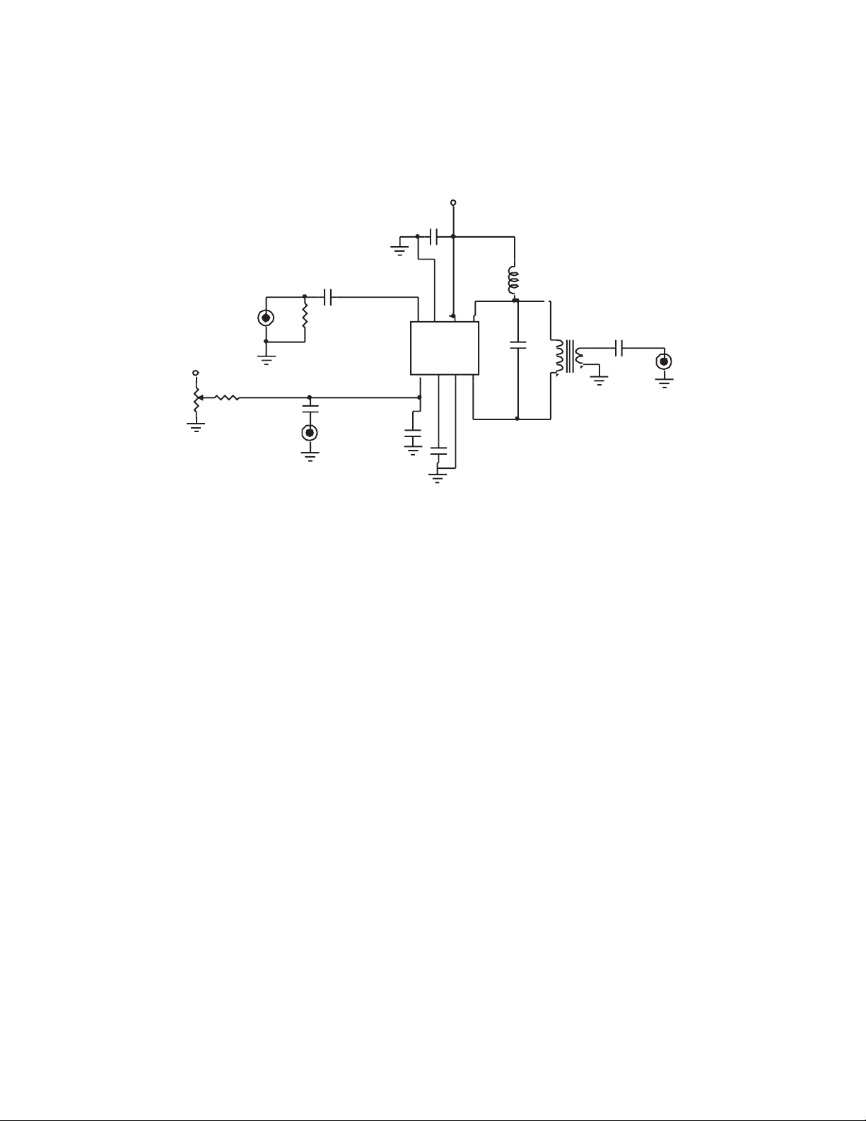
Typical application of a AM
Modulator using ML1350
V1
12V
+V
C4
.1uF
C1
220pF
C2
.1uF
nifr
dng
3
4
ML1350
6
5
cga
C3
.1uF
ccv
2
7
nifr
dng
P1
R2
50
C7
1uF
P2
L2
U2
1uH
C5
47pF
T1
C6
470pF
RF out
P3
tuof
r
1
8
t
u
ofr
www.lansdale.comPage 5 of 6 Issue A
Page 6
ML1350
NOTE 2
–T–
SEATING
PLANE
H
58
–B–
14
F
–A–
C
N
D
K
G
0.13 (0.005) B
M
T
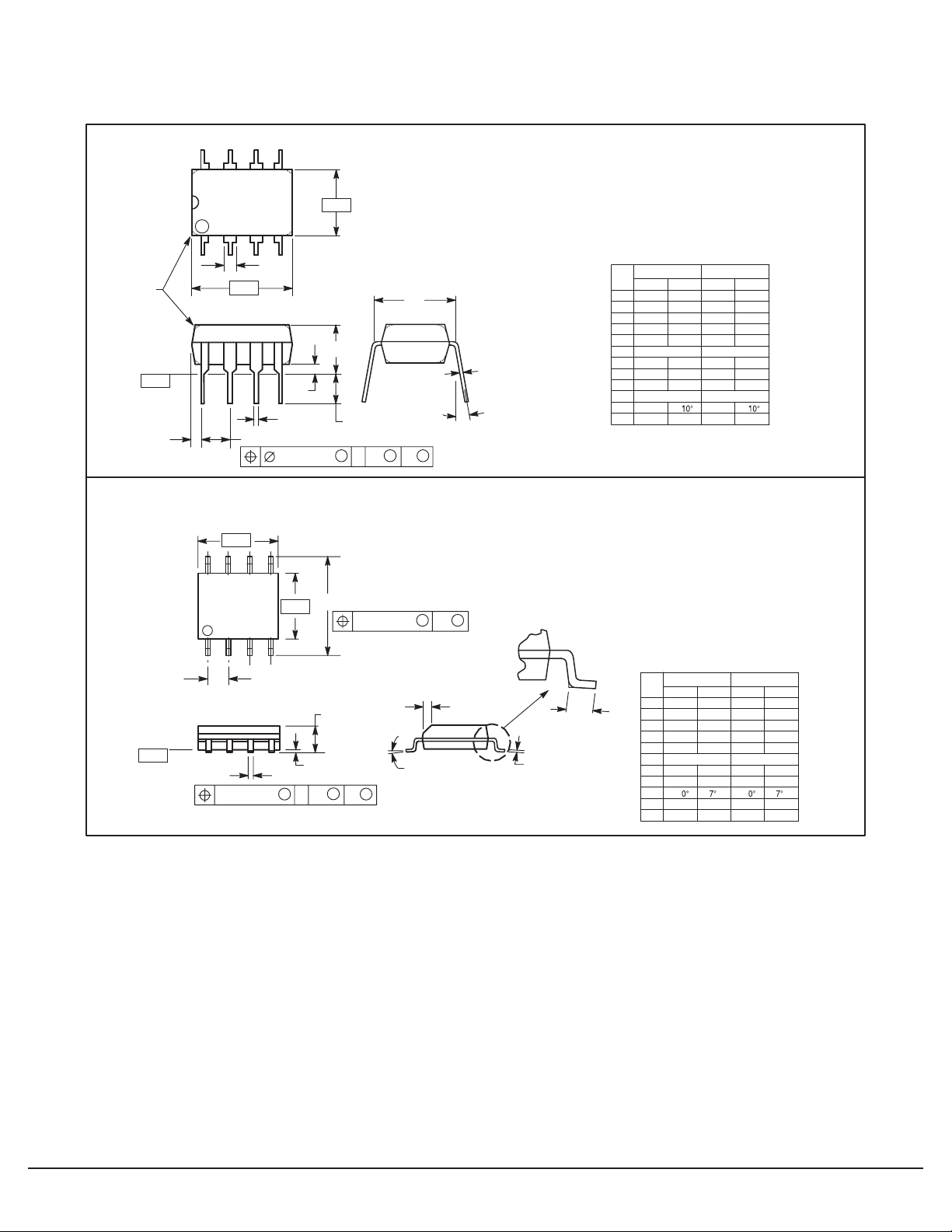
OUTLINE DIMENSIONS
P DIP 8 = PP
(ML1350PP)
PLASTIC PACKAGE
CASE 626–05
ISSUE K
L
J
M
M
A
M
LANSDALE Semiconductor, Inc.
NOTES:
1. DIMENSION L TO CENTER OF LEAD WHEN
FORMED PARALLEL.
2. PACKAGE CONTOUR OPTIONAL (ROUND OR
SQUARE CORNERS).
3. DIMENSIONING AND TOLERANCING PER ANSI
Y14.5M, 1982.
DIM MIN MAX MIN MAX
A 9.40 10.16 0.370 0.400
B 6.10 6.60 0.240 0.260
C 3.94 4.45 0.155 0.175
D 0.38 0.51 0.015 0.020
F 1.02 1.78 0.040 0.070
G 2.54 BSC 0.100 BSC
H 0.76 1.27 0.030 0.050
J 0.20 0.30 0.008 0.012
K 2.92 3.43 0.115 0.135
L 7.62 BSC 0.300 BSC
M ––– –––
N 0.76 1.01 0.030 0.040
INCHESMILLIMETERS
–T–
–A–
58
4X P
–B–
14
G
C
SEATING
PLANE
8X D
K
0.25 (0.010)MB
SS
A0.25 (0.010)MTB
SO 8 = -5P
(ML1350-5P)
PLASTIC PACKAGE
CASE 751–05
(SO–8)
ISSUE N
M
R
X 45°
M
NOTES:
1. DIMENSIONING AND TOLERANCING PER
ANSI Y14.5M, 1982.
2. CONTROLLING DIMENSION: MILLIMETER.
3. DIMENSIONS A AND B DO NOT INCLUDE
MOLD PROTRUSION.
4. MAXIMUM MOLD PROTRUSION 0.15 (0.006)
PER SIDE.
5. DIMENSION D DOES NOT INCLUDE DAMBAR
PROTRUSION. ALLOWABLE DAMBAR
PROTRUSION SHALL BE 0.127 (0.005) TOTAL
IN EXCESS OF THE D DIMENSION AT
MAXIMUM MATERIAL CONDITION.
DIM MIN MAX MIN MAX
F
J
A 4.80 5.00 0.189 0.196
B 3.80 4.00 0.150 0.157
C 1.35 1.75 0.054 0.068
D 0.35 0.49 0.014 0.019
F 0.40 1.25 0.016 0.049
G 1.27 BSC 0.050 BSC
J 0.18 0.25 0.007 0.009
K 0.10 0.25 0.004 0.009
M
P 5.80 6.20 0.229 0.244
R 0.25 0.50 0.010 0.019
INCHESMILLIMETERS
Lansdale Semiconductor reserves the right to make changes without further notice to any products herein to improve reliability, function or design. Lansdale does not assume any liability arising out of the application or use of any product or circuit
described herein; neither does it convey any license under its patent rights nor the rights of others. “Typical” parameters which
may be provided in Lansdale data sheets and/or specifications can vary in different applications, and actual performance may
vary over time. All operating parameters, including “Typicals” must be validated for each customer application by the customer’s
technical experts. Lansdale Semiconductor is a registered trademark of Lansdale Semiconductor, Inc.
www.lansdale.comPage 6 of 6 Issue A
 Loading...