

Page 1
www.lansdale.comPage 1 of 11 Issue 0
ML13135
FM Communications
Receiver; Dual Conversion
Narrowband FM Receiver
Legacy Device: Motorola MC13135
The ML13135 is the second generation of single chip, dual conversion
FM communications receivers developed by Motorola. Major
improvements in signal handling, RSSI and first oscillator operation
have been made. In addition, recovered audio distortion and audio
drive have improved. These receivers offer low noise, high gain and
stability over a wide operating voltage range, and Lansdale is pleased
to continue to offer them.
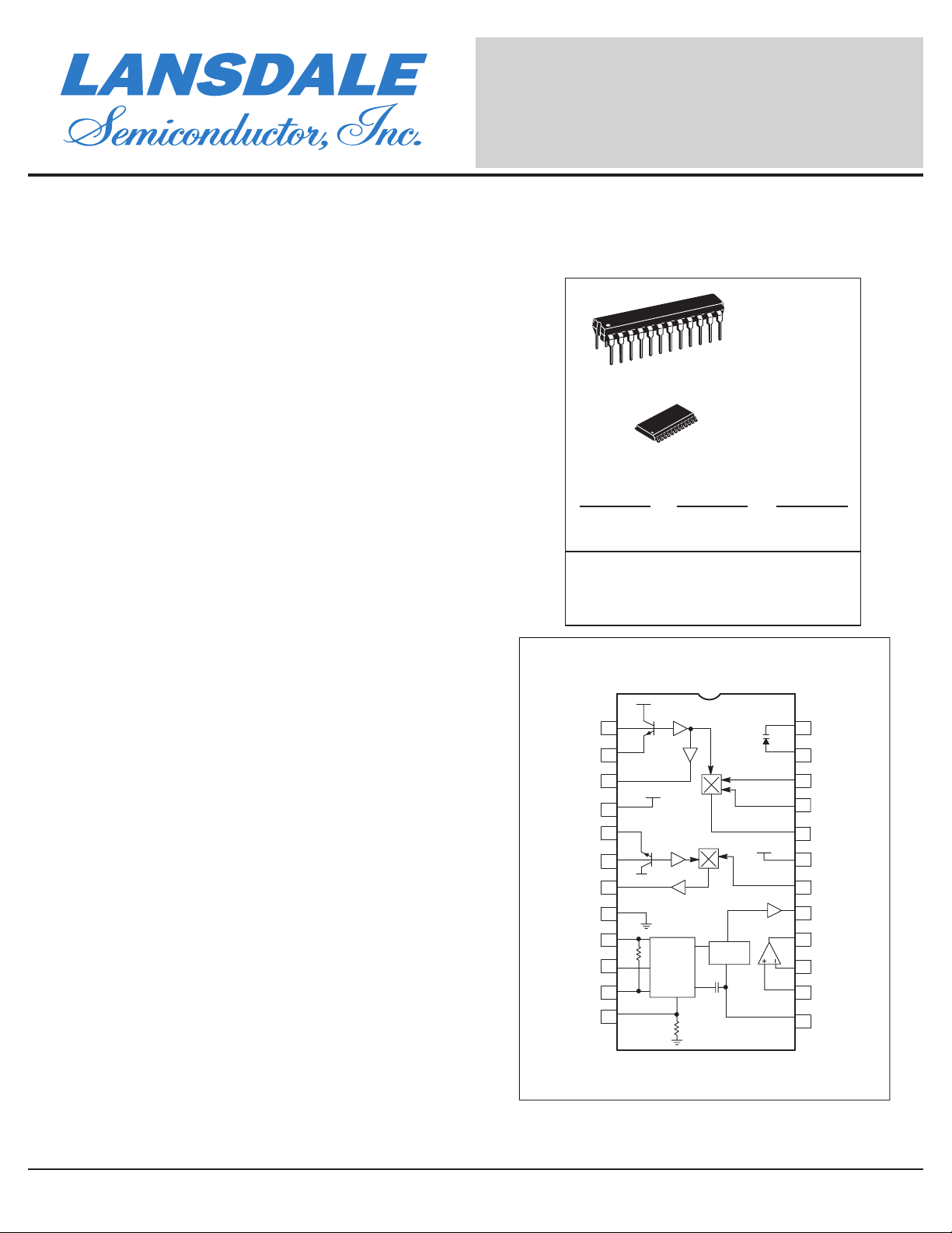
The ML13135 includes a Colpitts oscillator, VCO tuning diode, low
noise first and second mixer and LO, high gain limiting IF, and RSSI.
The ML13135 is designed for use with an LC quadrature detector and
has an uncommitted op amp that can be used either for an RSSI buffer
or as a data comparator.
This device can be used as a stand–alone VHF receiver or as the
lower IF of a triple conversion system. Applications include cordless
telephones, short range data links, walkie–talkies, low cost land
mobile, amateur radio receivers, baby monitors and scanners.
OPERATING FEATURES
• Complete Dual Conversion FM Receiver – Antenna to Audio Output
• Input Frequency Range – 200 MHz
• Voltage Buffered RSSI with 70 dB of Usable Range
• Low Voltage Operation – 2.0 to 6.0 Vdc (2 Cell NiCad Supply)
• Low Current Drain – 3.5 mA Typ
• Low Impedance Audio Output < 25 Ω
• VHF Colpitts First LO for Crystal or VCO Operation
• Isolated Tuning Diode
• Buffered First LO Output to Drive CMOS PLL Synthesizer
• Operating Temperature Range TA= –40° to +85°C
P DIP 24 = LP
24
1
24
1
CROSS REFERENCE/ORDERING INFORMATION
MOTOROLA
P DIP 24 MC13135P ML13135LP
SO 24 MC13135DW ML13135-6P
PLASTIC PACKAGE
CASE 724
SO 24 = -6P
CASE 751E
(SO–24L)
LANSDALEPACKAGE
Note: Lansdale lead free (Pb) product, as it
becomes available, will be identified by a part
number prefix change from ML to MLE.
1st LO Base
1st LO Emitter
1st LO Out
VCC1
2nd LO Emitter
2nd LO Base
2nd Mixer Out
V
EE
Limiter In
Decouple 1
Decouple 2
RSSI
The device contains 142 active transistors.
PIN CONNECTIONS
1st LO
1
2
3
VCC1
4
5
2nd LO
6
7
8
9
10
11
12
Limiter
Varicap
Demod
VCC2
AF
24
Varicap C
23
Varicap A
22
1st Mixer In 1
21
1st Mixer In 2
20
1st Mixer Out
VCC2
19
18
2nd Mixer In
17
Audio Out
16
Op Amp Out
15
Op Amp In –
14
Op Amp In +
13
Quad Coil
Page 2
www.lansdale.com
LANSDALE Semiconductor, Inc.
ML13135
Page 2 of 11 Issue 0
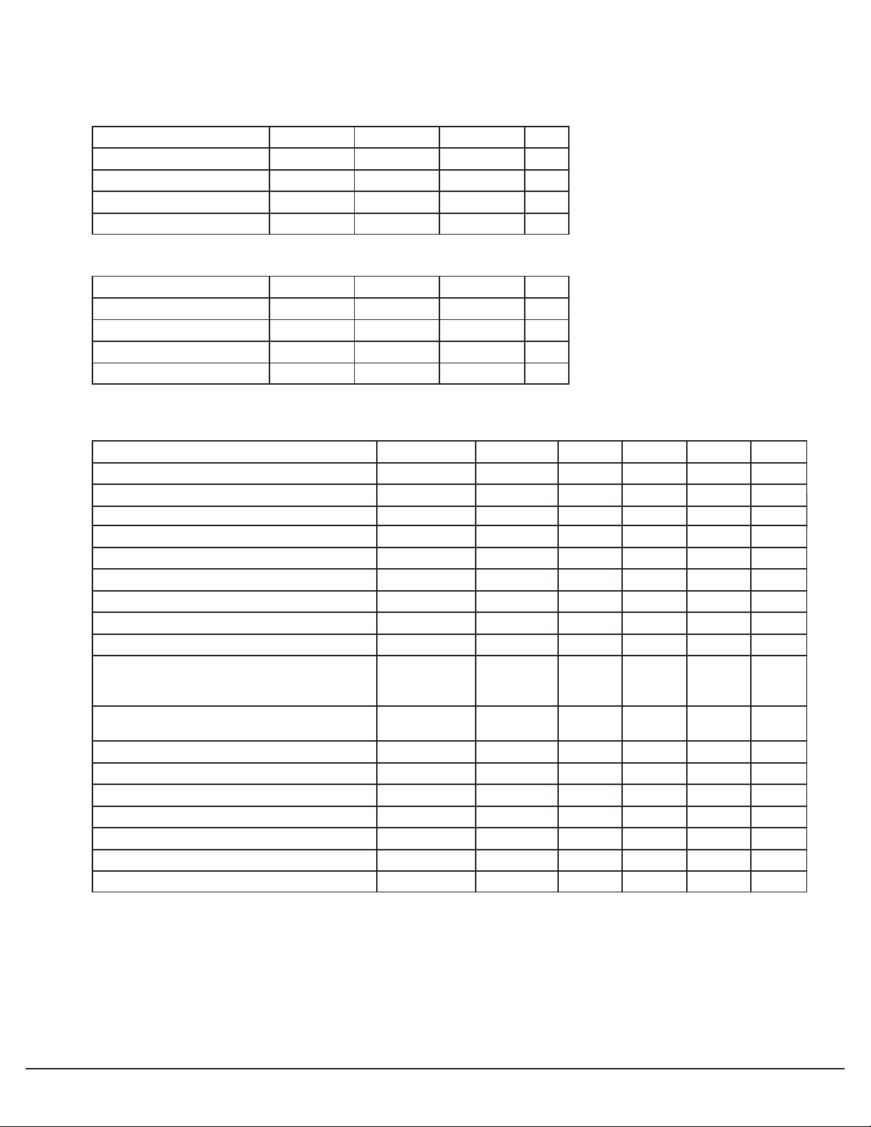
MAXIMUM RATINGS
Rating Pin Symbol Value Unit
Power Supply Voltage 4, 19 VCC (max) 6.5 Vdc
RF Input Voltage 22 RF
Junction Temperature – T
Storage Temperature Range – T
in
J
stg
1.0 Vrms
+150 °C
– 65 to +150 °C
RECOMMENDED OPERATING CONDITIONS
Rating Pin Symbol Value Unit
Power Supply Voltage 4, 19 V
Maximum 1st IF – f
Maximum 2nd IF – f
Ambient Temperature Range – T
CC
IF1
IF2
A
2.0 to 6.0 Vdc
21 MHz
3.0 MHz
– 40 to + 85 °C
ELECTRICAL CHARACTERISTICS (T
LO = 10.245 MHz, IF1 = 10.7 MHz, IF2 = 455 kHz, unless otherwise noted. All measurements performed in the test circuit of Figure 1.)
Characteristic
To tal Drain Current No Input Signal I
Sensitivity (Input for 12 dB SINAD) Matched Input V
Recovered Audio VRF = 1.0 mV AF
1st Mixer Conversion Gain VRF = – 40 dBm MX
2nd Mixer Conversion Gain VRF = – 40 dBm MX
First LO Buffered Output – V
To tal Harmonic Distortion VRF = – 30 dBm THD – 1.2 3.0 %
Demodulator Bandwidth – BW – 50 – kHz
RSSI Dynamic Range – RSSI – 70 – dB
First Mixer 3rd Order Intercept TOI
(Input) Matched – –17 –
Second Mixer 3rd Order Matched TOI
Intercept (RF Input) Input – –27 –
First LO Buffer Output Resistance – R
First Mixer Parallel Input Resistance – R – 722 – Ω
First Mixer Parallel Input Capacitance – C – 3.3 – pF
First Mixer Output Impedance – ZO – 330 – Ω
Second Mixer Input Impedance – Z
Second Mixer Output Impedance – ZO – 1.8 – kΩ
Detector Output Impedance – ZO – 25 – Ω
= 25°C, VCC = 4.0 Vdc, fo = 49.7 MHz, f
A
Condition Symbol Min Typ Max Unit
Unmatched – –11 –
= 1.0 kHz, Deviation = ±3.0 kHz, f
MOD
CC
SIN
O
gain1
gain2
LO
Mix1
Mix2
LO
I
– 4.0 6.0 mAdc
– 1.0 – µVrms
170 220 300
– 12 – dB
– 13 – dB
– 100 – mVrms
– – – Ω
– 4.0 – kΩ
1stLO
= 39 MHz, f
mVrms
2nd
dBm
dBm
Page 3
www.lansdale.comPage 3 of 11 Issue 0
LANSDALE Semiconductor, Inc.
ML13135
The recovered audio measurements for the ML13135 are
made with an LC quadrature detector. The typical recovered
audio will depend on the external circuit; either the Q of the
quad coil, or the RC matching network for the ceramic discriminator. See Figures 10 and 11 for additional information.
Since adding a matching circuit to the RF input increases the
signal level to the mixer, the third order intercept (TOI) point
is better with an unmatched input (50 Ω from Pin 21 to Pin
22). Typical values for both have been included in the
Electrical Characterization Table. TOI measurements were
taken at the pins with a high impedance probe/spectrum analyzer system. The first mixer input impedance was measured at
the pin with a network analyzer.
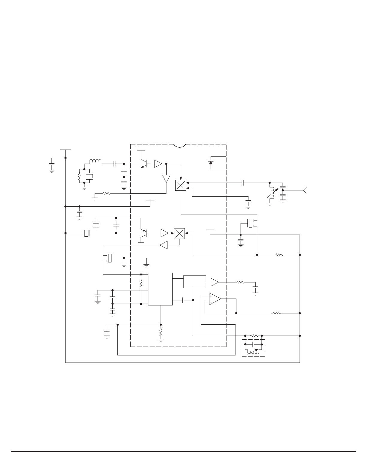
TEST CIRCUIT INFORMATION
Figure 1a. ML13135 Test Circuit
V
CC
µ
H
0.1
1.0 k
0.84
0.1
10.245
MHz Xtal
Ceramic
455 kHz
0.1
39.0
MHz
Filter
0.1
Xtal
5.0 k
120 p
0.1
0.01
20 p
5.0 p
50 p
0.1
12
1
2
3
4
5
6
7
8
9
10
11
1st LO
VCC1
2nd LO
Limiter
VCC2
AF
15
14
13
24
23
22
21
20
19
18
17
16
0.001
8.2 k
0.1
0.1
0.2
0.01
39 k
Figure 1.
µ
H
Ceramic
Filter
10.7 MHz
39 k
360
62 pF
180 p
RF
Input
Varicap
Demod
455 kHz
Quad
Coil
Page 4
www.lansdale.comPage 4 of 11 Issue 0
LANSDALE Semiconductor, Inc.
ML13135
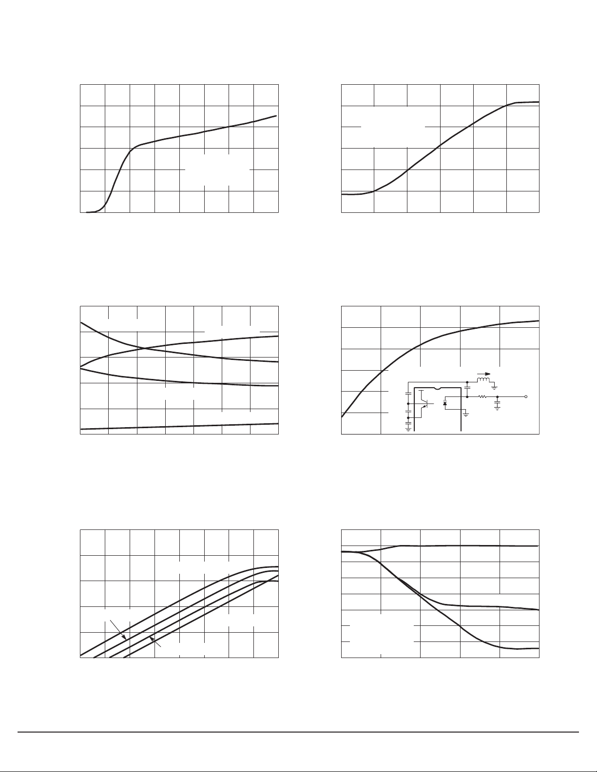
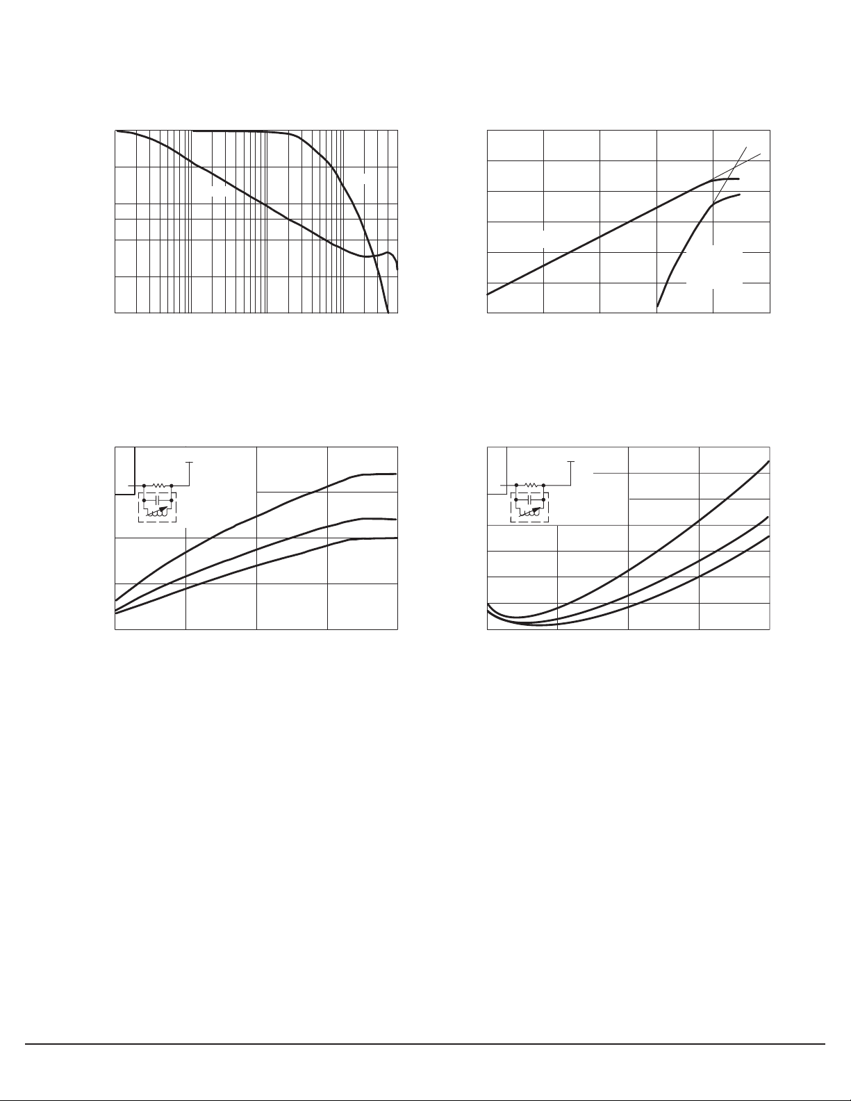
Figure 2. Supply Current versus Supply Voltage Figure 3. RSSI Output versus RF Input
6.0
1400
)Am( TNERRUC YLPPUS ,
5.0
4.0
3.0
RFin = 49.7 MHz
2.0
CC
1.0
I
0
0
1.0 2.0 3.0 4.0 5.0 6.0 7.0 8.0
f
MOD
f
DEV
VCC, SUPPLY VOLTAGE (V)
Figure 4. Varactor Capacitance, Resistance
)Fp( ECNATICAPAC LELLARAP TNE
25
CP, f = 150 MHz
20
15
10
LAV
5.0
I
U
Q
E
,
0
P
C
1.0 1.5 2.0 2.5 3.0 3.5 4.0
0.5
VB, VARACTOR BIAS VOLTAGE, V
versus Bias Voltage
CP, f = 50 MHz
Pin24
= 1.0 kHz
±
3.0 kHz
=
RP, f = 50 MHz
RP, f = 150 MHz
to V
Pin 23
(Vdc)
10
8.0
6.0
4.0
2.0
0
1200
)21
n
i
P ,
1000
c
dV
m
( TUPTU
O
ISSR
800
600
VCC = 4.0 V
RFin = 49.67 MHz
f
= 1.0 kHz
MOD
±
3.0 kHz
f
=
DEV
400
200
–140
–120 –100 – 80 – 60 – 40 – 20
RF INPUT (dBm)
Figure 5. Oscillator Frequency
) k( ECNATSISER LELLARAP TNELAVIUQE ,
Ω
48.0
47.5
)
z
47.0
HM( YCNE
46.5
U
QERF
46.0
,
f
45.5
45.0
P
R
1.0
versus Varactor Bias
0.61
µ
H
500 p
500 p
1
27 p
2
5.0 p
2.0 3.0 4.0 5.0 6.0
VB, VARACTOR BIAS VOLTAGE (Vdc)
1st LO
Varicap
24
1.0 M
23
Ω
0.2µF
V
B
30
10
)mBd( R
–10
E
WOP
–30
First Mixer Output
–50
–70
–100
Figure 6. Signal Levels versus RF Input
Second Mixer Output
First Mixer Input
Second Mixer Input
–90 –80 –70 –60 –50 –40 –30 –20
RFin, RF INPUT (dBm)
)
Bd(
R
M
A
D
N
A
,N
,N+
S
10
–10
–20
–30
–40
–50
–60
–70
–130
Figure 7. Signal + Noise, Noise, and
0
VCC = 4.0 Vdc
RFin = 49.67 MHz
f
MOD
f
DEV
AM Rejection versus Input Power
S + N
S + N 30% AM
= 1.0 kHz
±
3.0 kHz
=
–110 – 90 – 70 – 50 – 30
RFin, RF INPUT (dBm)
N
Page 5
www.lansdale.comPage 5 of 11 Issue 0
LANSDALE Semiconductor, Inc.
ML13135
)Bd( NIAG ,
V
A
2000
) Vm( OIDUA DEREVOCER ,AR
pp
1500
1000
50
30
10
–10
–30
–50
0
10 k
Figure 8. Op Amp Gain and Phase
versus Frequency
Gain
100 k 1.0 M 10 M
f, FREQUENCY (Hz)
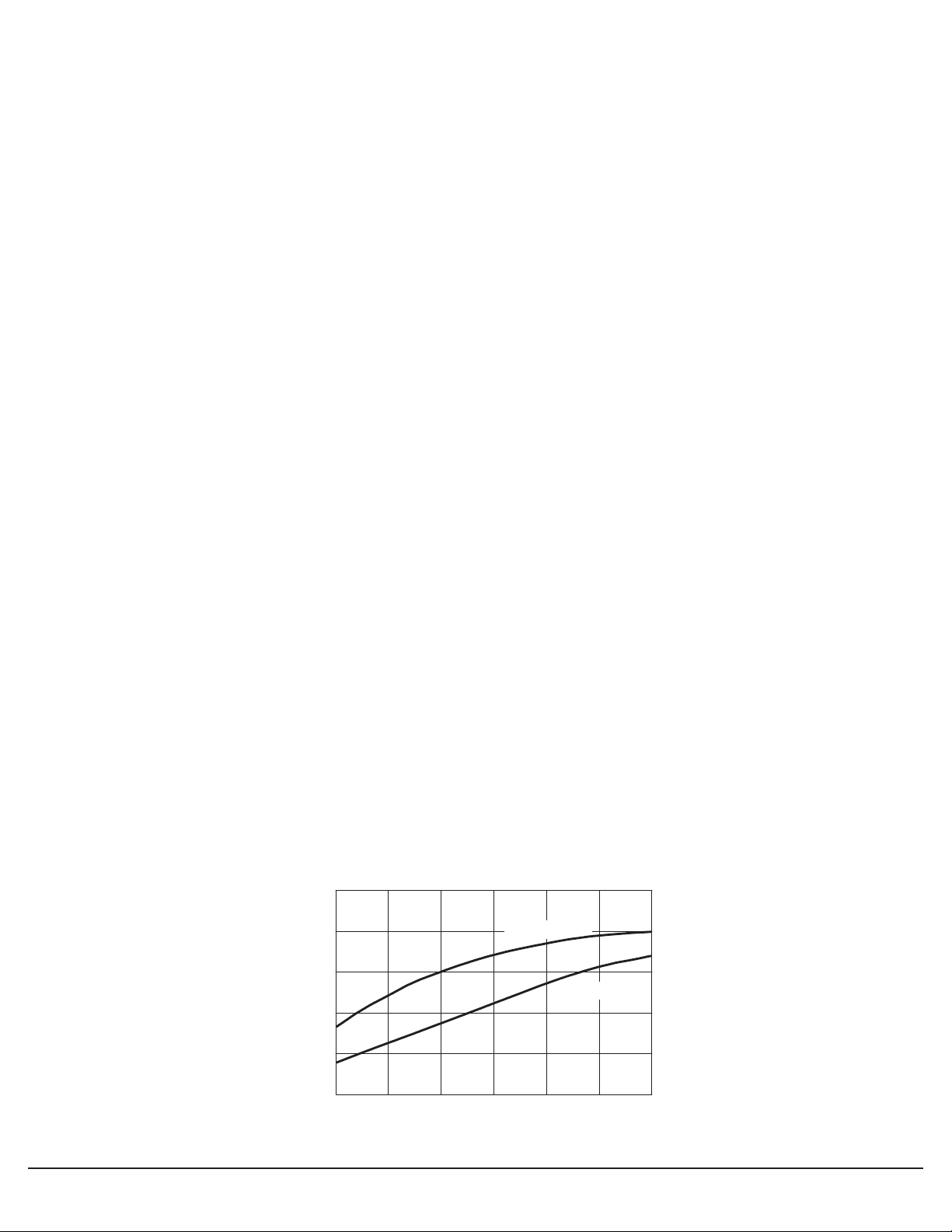
Figure 10. Recovered Audio versus
Deviation for ML13135
V
CC
R
13
455 kHz
Quad Coil
Toko 7MC–8128Z
Phase
R = 68 k
R = 47 k
R = 39 k
Figure 9. First Mixer Third Order Intermodulation
(Unmatched Input)
80
120
160
200
240
280
20
)SEERGED( ESAHP SSECXE ,
φ
)
Bd
(
–20
T
UP
TUO
–40
REX
–60
I
M
–80
–100
0
Desired Products
–100
3rd Order
Intermod
Products
–80 –60 –40 –20 0
RF INPUT (dBm)
Figure 11. Distortion versus
Deviation for ML13135
8.0
)%( NOITROTSID CINOMRAH L
Ω
Ω
Ω
7.0
6.0
5.0
4.0
13
V
CC
R
455 kHz
Quad Coil
Toko 7MC–8128Z
R = 68 k
R = 47 k
Ω
Ω
500
3.0
A
TOT ,DHT
2.0
0
±
1.0
±
3.0
±
5.0
f
, DEVIATION (kHz)
DEV
±
7.0
±
9.0
1.0
1.0
±
±
3.0
f
DEV
R = 39 k
Ω
±
5.0
, DEVIATION (kHz)
±
7.0
±
9.0
Page 6
www.lansdale.comPage 6 of 11 Issue 0
LANSDALE Semiconductor, Inc.
ML13135
The ML13135 is a complete dual conversion receiver. This
includes two local oscillators, two mixers, a limiting IF amplifier and detector, and an op amp. It will provide a voltage
buffered RSSI with 70 dB of usable range, isolated tuning
diode and buffered LO output for PLL operation, and a separate VCCpin for the first mixer and LO. Improvements have
been made in the temperature performance of both the recovered audio and the RSSI.
V
CC
Two separate VCClines enable the first LO and mixer to
continue running while the rest of the circuit is powered down.
They also isolate the RF from the rest of the internal circuit.
Local Oscillators
The local oscillators are grounded collector Colpitts, which
can be easily crystal–controlled or VCO controlled with the
on–board varactor and external PLL. The first LO transistor is
internally biased, but the emitter is pinned–out and IQ can be
increased for high frequency or VCO operation. The collector
is not pinned out, so for crystal operation, the LO is generally
limited to 3rd overtone crystal frequencies; typically around 60
MHz. For higher frequency operation, the LO can be provided
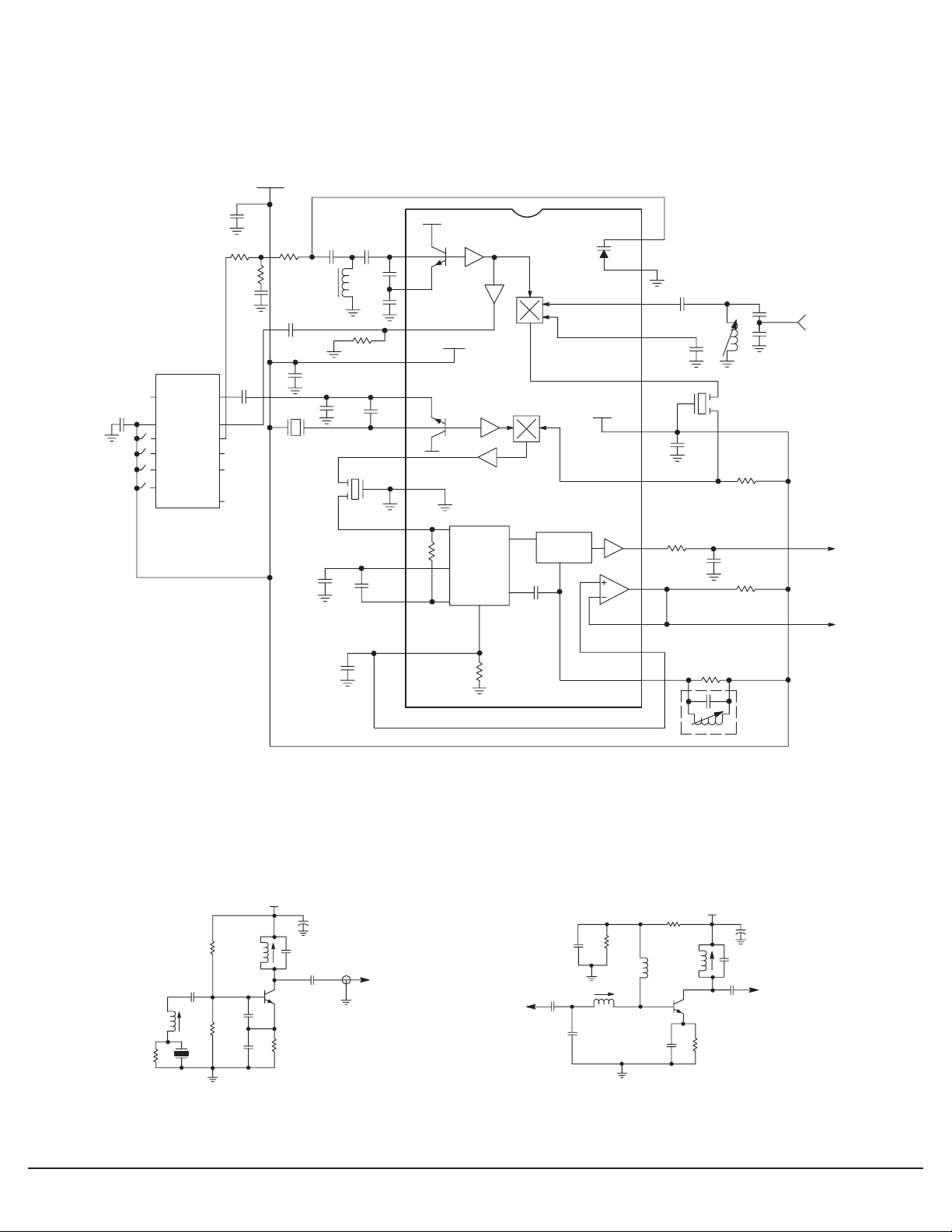
externally as shown in Figure 16.
Buffer
An amplifier on the 1st LO output converts the single–ended
LO output to a differential signal to drive the mixer. Capacitive
coupling between the LO and the amplifier minimizes the
effects of the change in oscillator current on the mixer.
Buffered LO output is pinned–out at Pin 3 for use with a PLL,
with a typical output voltage of 320 mVpp at VCC= 4.0 V and
with a 5.1 k resistor from Pin 3 to ground. As seen in Figure
14, the buffered LO output varies with the supply voltage and
a smaller external resistor may be needed for low voltage operation. The LO buffer operates up to 60 MHz, typically. Above
60 MHz, the output at Pin 3 rolls off at approximately 6.0 dB
per octave. Since most PLLs require about 200 mVpp drive, an
external amplifier may be required.
Mixers
The first and second mixer are of similar design. Both are
double balanced to suppress the LO and input frequencies to
give only the sum and difference frequencies out. This configuration typically provides 40 to 60 dB of LO suppression. New
design techniques provide improved mixer linearity and third
order intercept without increased noise. The gain on the output
of the 1st mixer starts to roll off at about 20 MHz, so this
receiver could be used with a 21 MHz first IF. It is designed
for use with a ceramic filter, with an output impedance of 330
Ω. A series resistor can be used to raise the impedance for use
with a crystal filter, which typically has an input impedance of
4.0 kΩ. The second mixer input impedance is approximately
4.0 kΩ; it requires an external 360 Ω parallel resistor for use
with a standard ceramic filter.
Limiting IF Amplifier and Detector
The limiter has approximately 110 dB of gain, which starts
rolling off at 2.0 MHz. Although not designed for wideband
operation, the bandwidth of the audio frequency amplifier has
been widened to 50 kHz, which gives less phase shift and
enables the receiver to run at higher data rates. However, care
should be taken not to exceed the bandwidth allowed by local
regulations.
The ML13135 is designed for use with an LC quadrature
detector, and does not have sufficient drive to be used with a
ceramic discriminator. The discriminators and the external
matching circuit will affect the distortion and recovered audio.
RSSI/Op Amp
The Received Signal Strength Indicator (RSSI) on the
ML13135 has about 70 dB of range. The resistor needed to
translate the RSSI current to a voltage output has been included on the internal circuit, which gives it a tighter tolerance. A
temperature compensated reference current also improves the
RSSI accuracy over temperature. On the ML13135, the op amp
is not connected internally and can be used for the RSSI or as
a data slicer (see Figure 17c).
CIRCUIT DESCRIPTION
Figure 14. Buffered LO Output Voltage
versus Supply Voltage
600
500
)
pp
Vm( TUP
400
TU
300
O
200
100
2.5
3.0 3.5 4.0 4.5 5.0 5.5
VCC, SUPPLY VOLTAGE (Vdc)
R
Pin3
= 3.0 k
R
Pin3
Ω
= 5.1 k
Ω
Page 7
www.lansdale.comPage 7 of 11 Issue 0
LANSDALE Semiconductor, Inc.
ML13135
Figure 15. PLL Controlled Narrowband FM Receiver at 46/49 MHz
0.1
OSC
OSC
Out
Fin1
VDD
D0
PD1
D1
PD2
D2
LD
D3
VSS
Fin2
ML145168
1
2
3
4
5
6
7
8
9
10
11
ML13135
1st LO
VCC1
2nd LO
Limiter
Varicap
Demod
VCC2
AF
24
23
22
21
20
19
18
17
16
15
0.001
0.01
1.0 k
0.1
0.15
0.2
µ
H
Ceramic
10.7 MHz
10 k
Filter
360
62 pF
150 pF
Recovered
RF
Input
Audio
RSSI
Output
V
CC
0.1
500 p
0.1
Filter
µ
H
500 p
5.1 k
120 p
27 p
5.0 p
50 p
0.1
47 k
1.0
3.0 p
100 k
0.68
0.01
10.245
MHz Xtal
Ceramic
455 kHz
0.1
2.7 k
In
0.82
1.0 k
12
0.1
14
13
68 k
455 kHz
Quad Coil
Figure 16. 144 MHz Single Channel Application Circuit
1st LO
External Oscillator Circuit
V
CC
+
1.0µF
15 k
100 p
µ
5.6 k
X1
L1
68 p
43 p
Q1
470
15 p
1000p
f
=
osc
133.755 MHz
MPS5179
Q1 –
44.585 MHz 3rd Overtone
X1 –
Series Resonant Crystal
µ
L1 –
H Inductor
0.078
(Coilcraft Part # 146–02J08)
RF Input
Preamp for ML13135 at 144.455 MHz
V
15 k
L2
5.1 k
1.0
3300 p
L3
µ
Q1
3300 p
470 p
12 p
CC
470
39 p
+
12 p
1.0µF
To Mixer
Q1 –
L2 –
L3 –
MPS5179
µ
H
0.05
µ
H
0.07
Page 8
www.lansdale.comPage 8 of 11 Issue 0
LANSDALE Semiconductor, Inc.
ML13135
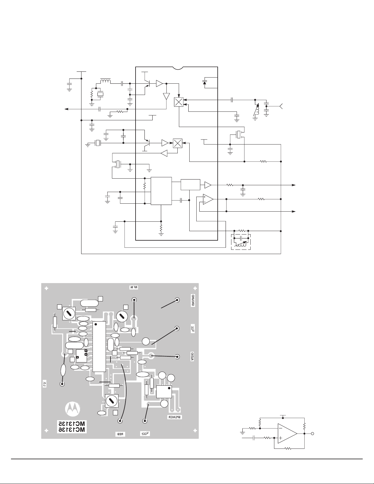
Legacy Applications Information
Figure 17a. Single Channel Narrowband FM Receiver at 49.7 MHz
1.0
Buffered LO
Output
ML13135
V
CC
+
1.0 k
µ
H
1.0
39 MHz
Xtal
0.01
0.1
10.245 MHz
Xtal
Ceramic
2200 p
5.1 k
120 p
27 p
5.0 p
50 p
1
2
3
4
5
6
7
8
1st LO
VCC1
2nd LO
Varicap
VCC2
24
23
22
21
20
19
18
0.001
0.01
0.2
0.1
µ
H
Ceramic
Filter
10.7 MHz
62 pF
150 p
360
Figure 17.
RF Input
Ω
Source
50
Filter
455 kHz
0.1
0.1
0.1
9
10
11
12
Limiter
Demod
AF
17
16
15
14
13
1.0 k
0.15
Recovered
Audio
10 k
RSSI
Output
39 k
455 kHz
Quad Coil
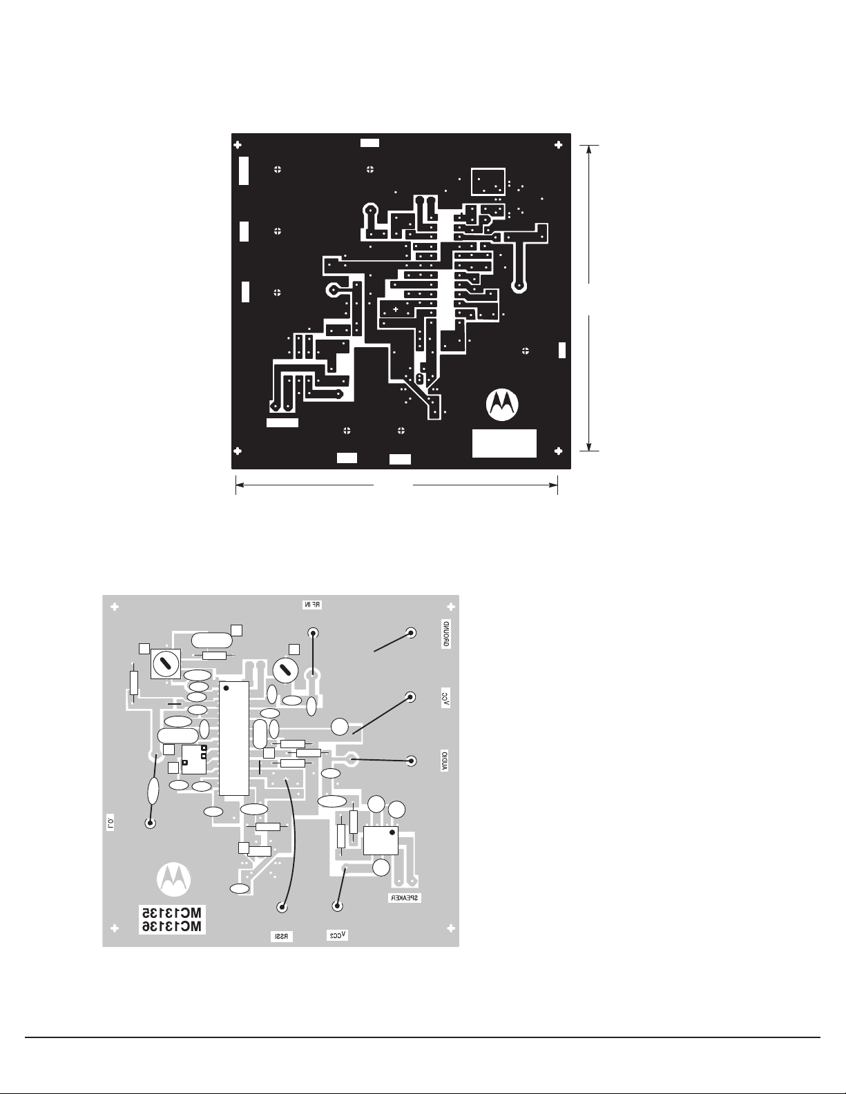
Figure 17b. PC Board Component View
2
39 MHz
120p
XT
5
0.1
2200p
27p
5p
0.1
CF
455 KHz
0.1
p0
5
XT
1.0 k
0.1
1
1
0
0.
62p
p
05
0.01
z
531
H
M
F
C
3
7.
1CM
01
7
39K
0.1
6
1
1
.0
360
1.0k
10k
3
k
1
.
5
10.245 MHz
4
10
.
0
0.15
0.22
NOTES: 1. 0.2 µH tunable (unshielded) inductor
2. 39 MHz Series mode resonant
3rd Overtone Crystal
3. 1.5 µH tunable (shielded) inductor
4. 10.245 MHz Fundamental mode crystal,
32 pF load
5. 455 kHz ceramic filter, muRata CFU 455B
or equivalent
6. Quadrature coil, Toko 7MC–8128Z (7mm)
1.0
+
or Toko RMC–2A6597HM (10mm)
7. 10.7 MHz ceramic filter, muRata SFE10.7MJ–A
or equivalent
10
+
+4.7
k
01
K
1
5
MC34119
+10
Figure 17c. Optional Data Slicer Circuit
(Using Internal Op Amp)
V
CC
20 k
V
in
(Pin 17)
20 k
0.001
10 k
14
15
16
10 k
FSK Data
Output
1.0 M
Page 9
www.lansdale.comPage 9 of 11 Issue 0
LANSDALE Semiconductor, Inc.
ML13135
Legacy Applications Information
Figure 18. PC Board Solder Side View
RF IN
DNUORG
CC
V
OIDUA
SPEAKER
″
52.3
.O.L
MC13135
V
CC2
RSSI
3.375
″
(Circuit Side View)
Figure 19. PC Board Component View
2
39 MHz
120p
XT
5
0.1
2200p
27p
5p
0.1
CF
455 KHz
0.1
p05
XT
1.0 k
0.1
1
100.
62p
0.01
z
6
H
31
M
FC
7.01
31
CM
7
270p
2.7k
6
0.1
p051
1.0k
0.15
0.22
1.0
+
10
+
+4.7
k0
1
K15
MC34119
+10
1.
0
360
10k
3
k1
.5
10.245 MHz
4
10
.
0
MC13136
NOTES: 1. 0.2 µH tunable (unshielded) inductor
2. 39 MHz Series mode resonant
3rd Overtone Crystal
3. 1.5 µH tunable (shielded) inductor
4. 10.245 MHz Fundamental mode crystal,
32 pF load
5. 455 kHz ceramic filter, muRata CFU 455B
or equivalent
6. Ceramic discriminator, muRata CDB455C34
or equivalent
7. 10.7 MHz ceramic filter, muRata SFE10.7MJ–A
or equivalent
Page 10
www.lansdale.comPage 10 of 11 Issue 0
LANSDALE Semiconductor, Inc.
ML13135
2
CC
V
k 0.4
81
k 0.4k 0.6
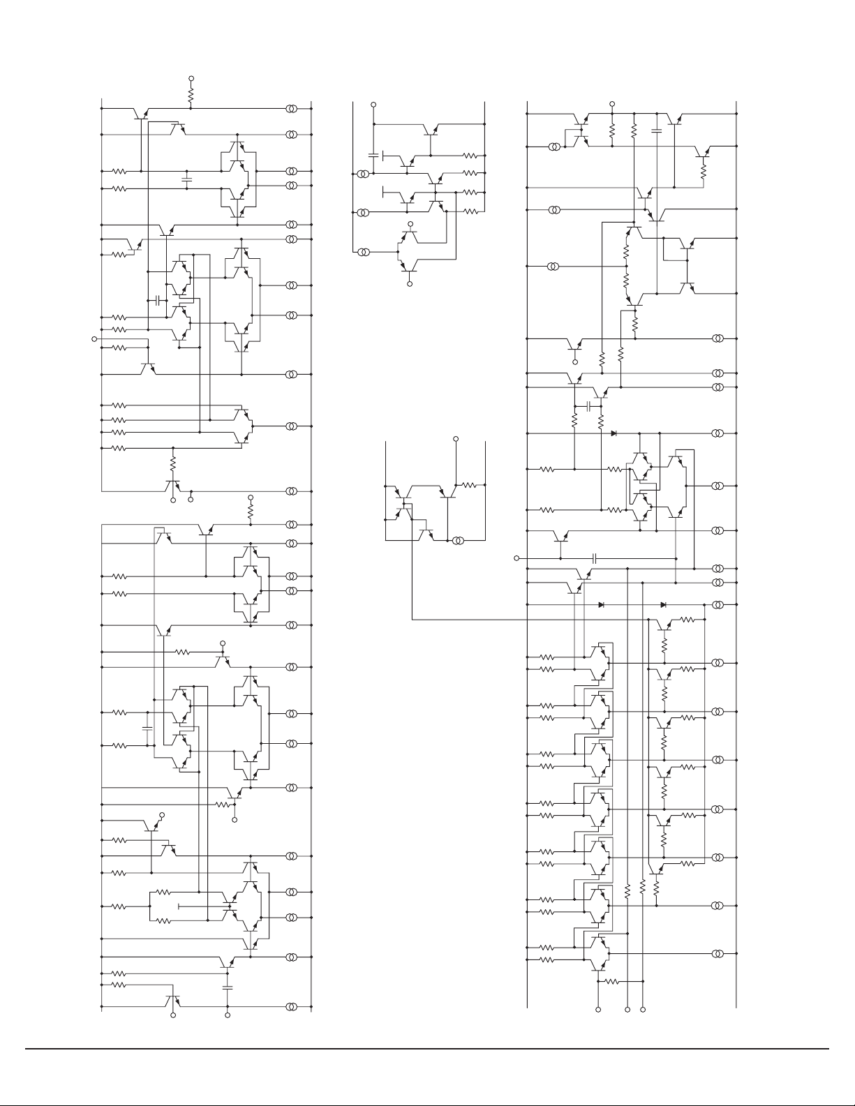
citamehcS lanretnI 53131LM .12 er
7
k 6.1
k 21
0
2
6
5
001
V
2
E
E
CC
61
V
rexiM dnoceSOL dnoceS
51
41
2
C
C
V
V
21
k 001
2
EE
V
C
C
V
pmA pO
saiB
EE
7
1
E
E
V
rei
f
i
l
p
m
A
oid
uA dn
a
rotcete
D
.sr
o
tsisnart evitc
p 0.5
31
u
gi
F
k
0
.
8
k 0.1
3
12
re
x
i
M
tsriFOL t
k
0
.
2
1
2
k 05
k 25
s
riF
a 2
41
s
n
ia
t
noc
ec
ive
d
s
ihT
re
i
fil
p
mA
FI g
n
itim
i
L
p
k 5
1
1
C
C
V
1
0.5
2
E
E
V
Figure 21.
k
0.2
2
CC
V
01
9
11
E
E
V
Page 11
www.lansdale.comPage 11 of 11 Issue 0
LANSDALE Semiconductor, Inc.
ML13135
Lansdale Semiconductor reserves the right to make changes without further notice to any products herein to improve reliability, function or design. Lansdale does not assume any liability arising out of the application or use of any product or circuit
described herein; neither does it convey any license under its patent rights nor the rights of others. “Typical” parameters which
may be provided in Lansdale data sheets and/or specifications can vary in different applications, and actual performance may
vary over time. All operating parameters, including “Typicals” must be validated for each customer application by the customer’s
technical experts. Lansdale Semiconductor is a registered trademark of Lansdale Semiconductor, Inc.
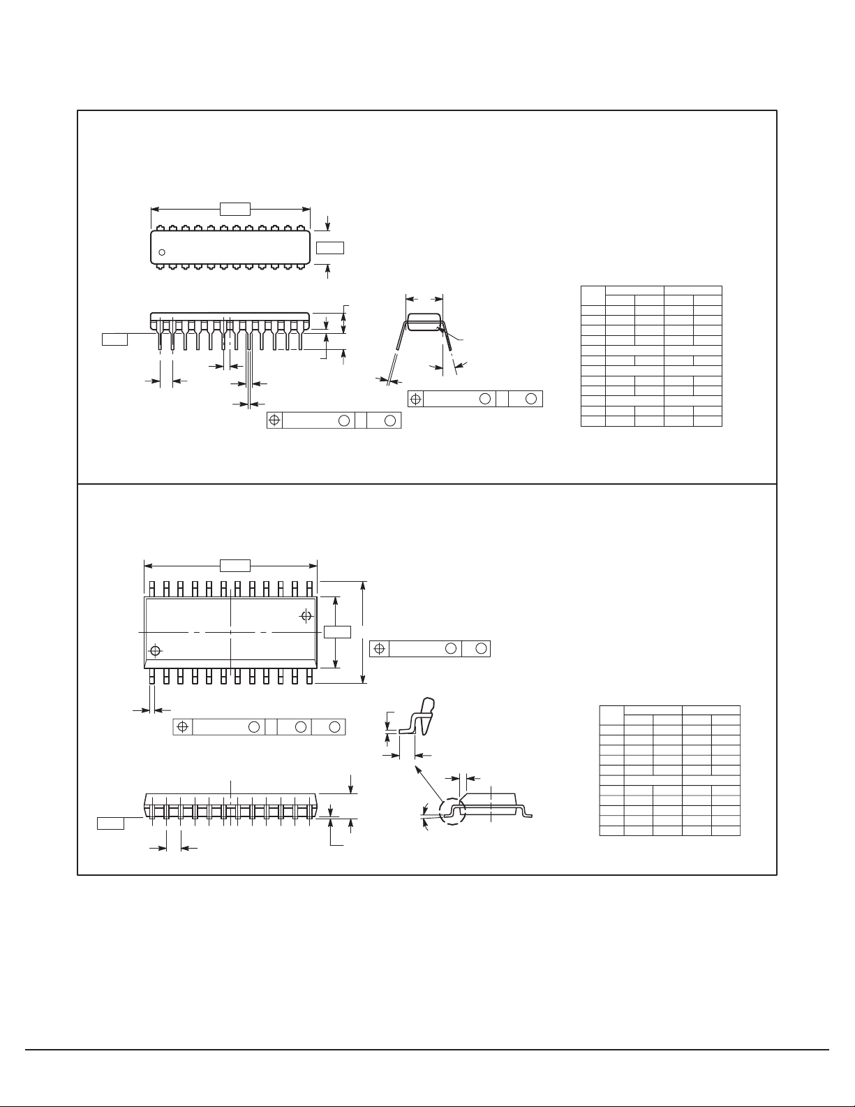
OUTLINE DIMENSIONS
P DIP 24 = LP
PLASTIC PACKAGE
(ML13135LP)
CASE 724–03
ISSUE D
–T–
SEATING
PLANE
–T–
SEATING
PLANE
–A–
1324
112
E
G
F
D
–B–
C
K
N
24 PL
0.25 (0.010) T A
M M
L
NOTE 1
M
J 24 PL
0.25 (0.010) T B
SO 24 = -6P
(ML13135-6P)
PLASTIC PACKAGE
CASE 751E–04
ISSUE E
–A–
24 13
–B–
P 12 PL
0.010 (0.25)
112
D 24 PL
0.010 (0.25) A B
M
T
S S
J
M M
B
F
C
G 22 PL
K
M
M M
R X 45°
NOTES:
1. CHAMFERED CONTOUR OPTIONAL.
2. DIMENSION L TO CENTER OF LEADS WHEN
FORMED PARALLEL.
3. DIMENSIONING AND TOLERANCING PER ANSI
Y14.5M, 1982.
4. CONTROLLING DIMENSION: INCH.
INCHES MILLIMETERS
MIN MINMAX MAX
DIM
A
1.230
B
0.250
C
0.145
D
0.015
E
0.050 BSC
F
0.040
0.100 BSC
G
J
0.007
K
0.110
0.300 BSC
L
M
0
°
N
0.020
NOTES:
1. DIMENSIONING AND TOLERANCING PER ANSI
Y14.5M, 1982.
2. CONTROLLING DIMENSION: MILLIMETER.
3. DIMENSIONS A AND B DO NOT INCLUDE
MOLD PROTRUSION.
4. MAXIMUM MOLD PROTRUSION 0.15 (0.006)
PER SIDE.
5. DIMENSION D DOES NOT INCLUDE DAMBAR
PROTRUSION. ALLOWABLE DAMBAR
PROTRUSION SHALL BE 0.13 (0.005) TOTAL IN
EXCESS OF D DIMENSION AT MAXIMUM
MATERIAL CONDITION.
DIM
A
B
C
D
F
G
J
K
M
P
R
31.25
15.54
7.60
2.65
0.49
0.90
0.32
0.29
8
10.55
0.75
6.35
3.69
0.38
1.27 BSC
1.02
2.54 BSC
0.18
2.80
7.62 BSC
0
°
0.51
°
32.13
0.601
0.292
0.093
0.014
0.016
0.009
0.005
0
°
0.395
0.010
6.85
4.44
0.51
1.52
0.30
3.55
15
1.01
°
1.265
0.270
0.175
0.020
0.060
0.012
0.140
15
°
0.040
MILLIMETERS INCHES
MIN MINMAX MAX
15.25
7.40
2.35
0.35
0.41
1.27 BSC 0.050 BSC
0.23
0.13
0
°
10.05
0.25
0.612
0.299
0.104
0.019
0.035
0.013
0.011
8
0.415
0.029
°
 Loading...