

Page 1
512 bit (64b x8) Serial Access TIMEKEEP ER® SRAM
COUNTERS for SECONDS, MINUTES,
HOURS, DAY, DATE, MONTH and YEARS
SOFTWARE CLOCK CALIBRATION
AUTOMATIC POWER-F AIL DETECT and
SWITCH CIRCUITRY
I2C BUS COMPATIB LE
56 BYTES of GENERAL PURPOSE RAM
ULTRA-LOW BATTERY SUPPLY CURRENT of
500nA
OPERATING TEMPERATURE:
– MK41T56: 0 to 70°C
– MKI41T56: –40 to 85°C
AUTOMATIC LEAP YEAR COMPENSATION
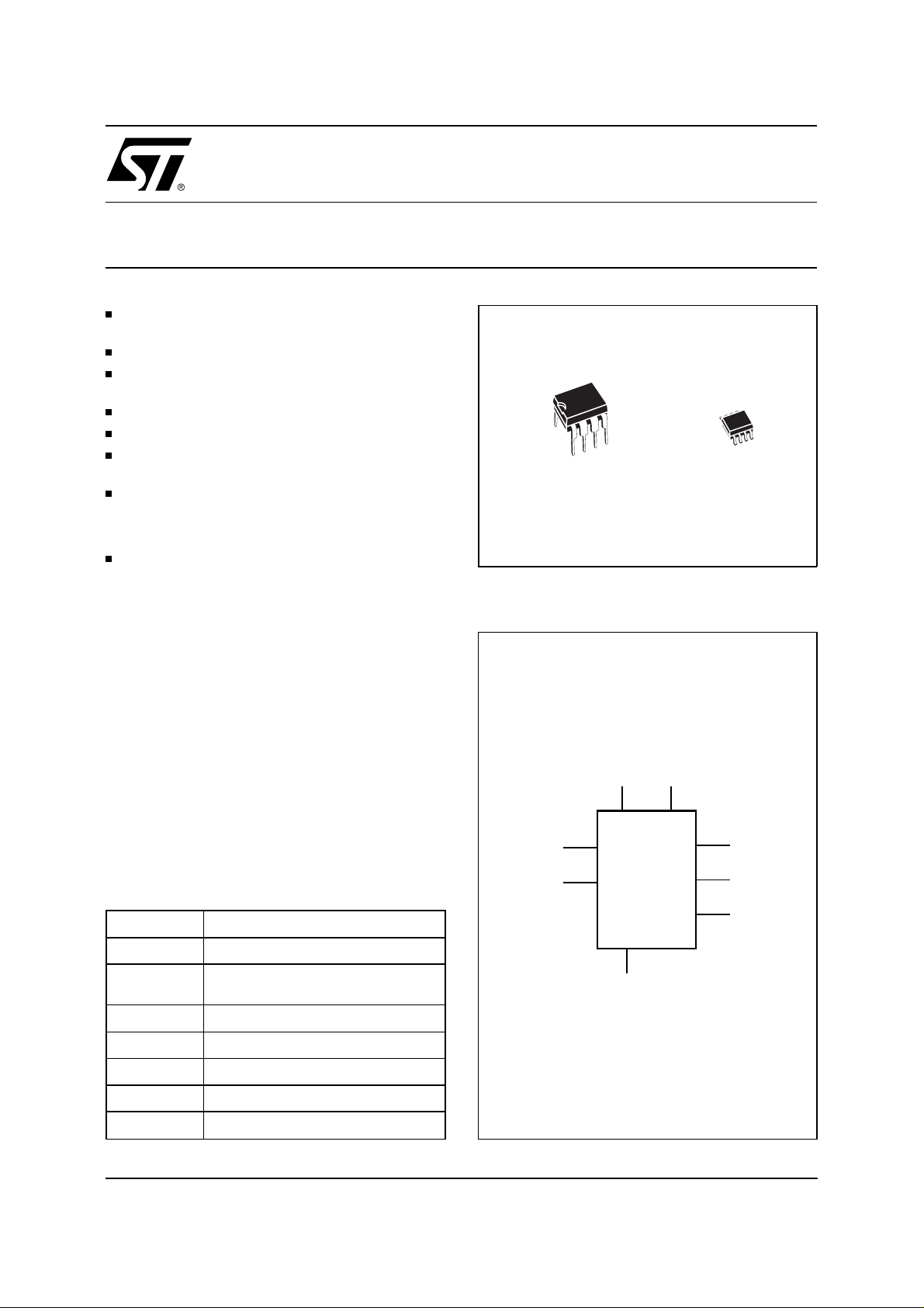
8
1
PSDIP8 (N)
0.4mm Frame
MK41T56
MKI41T56
8
1
SO8 (S)
150mil Width
DESCRIPTION
The MK41T56 TIME KEE PE R
®
is a low power 512
bit static CMOS RAM organized as 64 words by 8
bits. A built-in 32.768 kHz oscillator (external crystal
controlled) and the first 8 bytes of the RAM are used
for the clock/calendar function and are configured
in binary coded decimal (BCD) format. Addresses
and data are transferred serially via a two-line
bi-directional bus. The built-in addres s register is
incremented automatically after each write or read
data byte. The MK41T56 clock has a built-in power
sense circuit which detects power failures and
automatically switches to the battery supply during
power failures. The energy needed to sustain the
RAM and clock operations can be supplied from a
small lithium button cell.
T ab le 1. Signal Names
OSCI Oscillator Input
OCSO Oscillator Output
FT/OUT
SDA Serial Data Address Input / Output
SCL Serial Clock
Frequency Test / Output Driver
(Open Drain)
Figure 1. Logic Diagram
V
CC
OSCI
SCL
MK41T56
MKI41T56
V
SS
V
BAT
OSCO
SDA
FT/OUT
AI02304
V
BAT
V
CC
V
SS
March 1999 1/15
Battery Supply Voltage
Supply Voltage
Ground
Page 2
MK41T56, MKI41T56
Figure 2A. DIP Pin Connections
MK41T56
MKI41T56
OSCI V
1
2
BAT
SS
3
4
V
8
7
6
5
AI02305
FT/OUTOSCO
SCL
SDAV
CC
Figure 2B. SOIC Pin Connections
MK41T56
MKI41T56
OSCI V
1
2
V
BAT
SS
3
4
8
7
6
5
AI02306
FT/OUTOSCO
SCL
SDAV
CC
T ab le 2. Absolute Maximum Ratings
Symbol Parameter Value Unit
T
A
T
STG
V
IO
V
CC
I
O
P
D
Note:
Stresses greater than those listed under "Absolute Maximum Ratings" may cause permanent damage to the device. This is a stress
rating only and functional operation of the device at these or any other conditions above those indicated in the operational section of
this specification is not implied. Exposure to the absolute maximum rating conditions for extended periods of time may affect
reliability.
CAUTION: Negat i ve undershoots below –0.3 volts are not allowed on any pin while in the Battery Back-up mode.
Ambient Operating Temperature MK41T56
MKI41T56
0 to 70
–40 to 85
Storage T emper ature (VCC Off, Oscillator Off) –55 to 125 °C
Input or Output Voltages –0.3 to 7 V
Supply Voltage –0.3 to 7 V
Output Current 20 mA
Power Dissipation 0.25 W
°C
T ab le 3. Register Map
Address
D7 D6 D5 D4 D3 D2 D1 D0
0 ST 10 Seconds Seconds Seconds 00-59
1 X 10 Minutes Minutes Minutes 00-59
2 X X 10 Hours Hours Hour 00-23
3 X X X X X Day Day 01-07
4 X X 10 Date Date Date 01-31
5 X X X 10 M. Month Month 01-12
6 10 Years Years Y ear 00-99
7 OUT FT S Calibration Control
Keys: S
= SIGN Bit; FT = FREQUENCY TEST Bi t; ST = STOP Bi t;
2/15
Data
OUT
= Output level; X = Don’t care.
Function/Range
BCD Format
Page 3
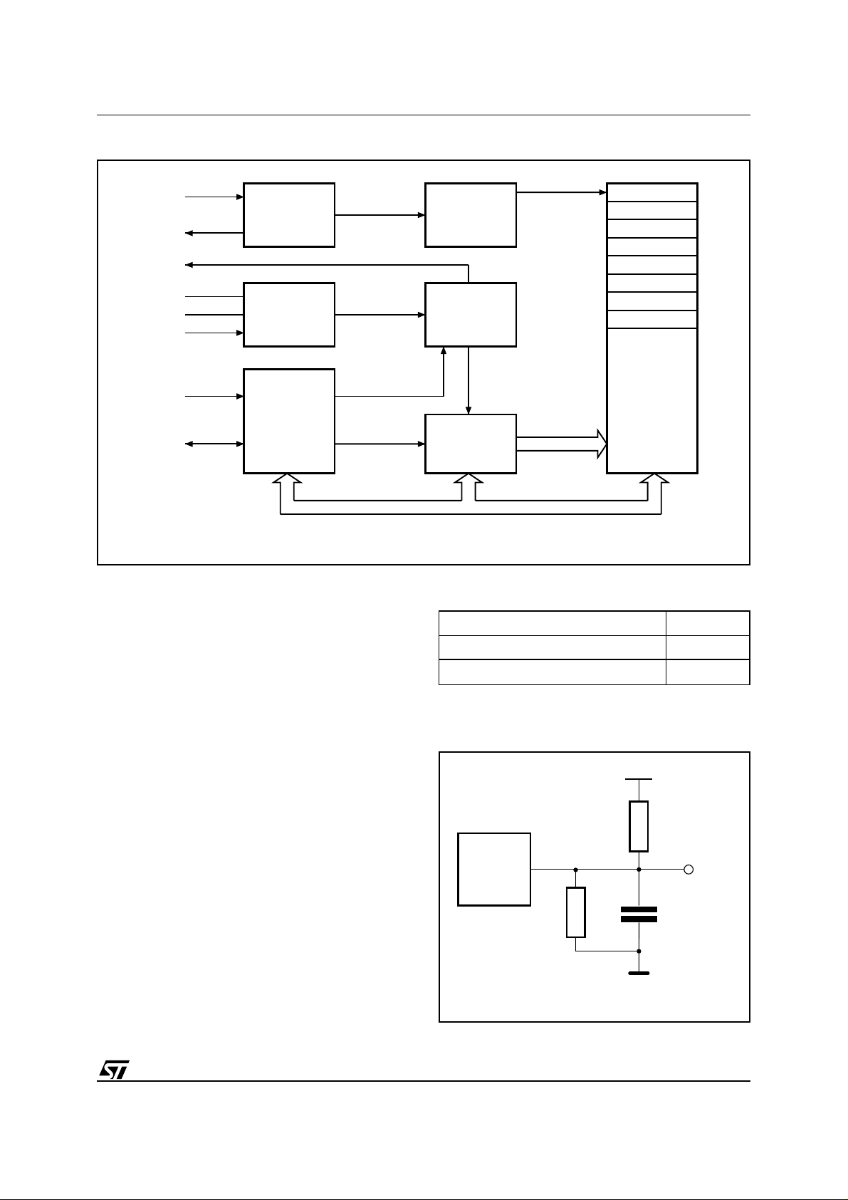
Figure 3. Block Diagram
MK41T56, MKI41T56
OSCI
OSCO
FT/OUT
V
CC
V
SS
V
BAT
SCL
SDA
DESCRIPTION
(cont’d)
OSCILLATOR
32.768 kHz
VOLTAGE
SENSE
and
SWITCH
CIRCUITRY
SERIAL
BUS
INTERFACE
1 Hz
DIVIDER
CONTROL
LOGIC
ADDRESS
REGISTER
SECONDS
MINUTES
HOURS
DAY
DATE
MONTH
YEAR
CONTROL
RAM
(56 x 8)
AI00586C
Table 4. AC Measurement Conditions
Data retention time is in excess of 10 years with a
50mAh 3V lithium cell. The MK41T56 is supplied in
8 pin Plastic Dual-in-Line and 8 lead Plastic SOIC
packages.
OPERATION
The MK41T56 clock operates as a slave dev ice on
the serial bus. Access is obtained by implementing
a start condition followed by the correct slave address (11010000). The 64 bytes contained in the
device can then be ac cessed sequentially in the
following order:
1. Seconds Register
2. Minutes Register
3. Hours Register
4. Day Register
5. Date Register
6. Month Register
7. Years Register
8. Control Register
9 to 64. RAM
Input Rise and Fall Times ≤ 5ns
Input Pulse Voltages 0 to 3V
Input and Output Timing Ref. Voltages 1.5V
Note that Output Hi-Z is defined as the point where data is no
longer driven.
Figure 4. AC Testing Load Circuit
5V
1.8kΩ
DEVICE
UNDER
TEST
1kΩ
CL includes JIG capacitance
OUT
CL = 100pF
AI01019
3/15
Page 4
MK41T56, MKI41T56
(1,2)
T ab le 5. Capacitance
= 25 °C, f = 1 MHz )
(T
A
Symbol Parameter Min Max Unit
C
IN
(2)
C
OUT
Notes:
1. Effective capacitance measured with power supply at 5V.
2. Sampled, not 100% tested.
3. Outputs deselected.
T ab le 6. DC Characteristics
= 0 to 70°C or –40 to 85°C; VCC = 4.5V to 5.5V)
(T
A
Input Capacitance (SCL) 7 pF
Output Capacitance (SDA, FT/OUT) 10 pF
Symbol Parameter Test Condition Min Typ Max Unit
I
LI
I
LO
I
CC1
I
CC2
V
IL
V
IH
V
OL
V
BAT
I
BAT
Note:
1. The RAYOV AC BR1225 or equivalent is recommended as the battery supply.
Input Leakage Current 0V ≤ VIN ≤ V
Output Leakage Current 0V ≤ V
OUT
≤ V
CC
CC
Supply Current SCL/SDA = VCC–0.3V 1 mA
Supply Current (Standby) 1 mA
Input Low Voltage –0.3 1.5 V
Input High Voltage 3 VCC + 0.8 V
Output Low Voltage IOL = 5mA, VCC = 4.5V 0.4 V
(1)
Battery Supply Voltage 2.6 3 3.5 V
T
= 25°C, VCC = 0V,
Battery Supply Current
A
Oscillator ON, V
BAT
= 3V
450 500 nA
±10 µA
±10 µA
T able 7. Power Down/Up Trip Points DC Characteristics
= 0 to 70°C or –40 to 85°C)
(T
A
(1)
Symbol Parameter Min Typ Max Unit
V
PFD
V
SO
Note:
1. All voltages referenced to V
T ab le 8. Crystal Electrical Characteristics
Power-fail Deselect Voltage 1.2 V
BAT
1.25 V
Battery Back-up Switchover Voltage V
.
SS
BAT
BAT
1.285 V
BAT
(Externally Supplied)
Symbol Parameter Min Typ Max Unit
f
O
R
S
C
Notes:
Load capacitors are integrated within the MK41T56. Cir cuit board layout considerations for the 32.768 kHz crystal of
Resonant Frequency 32.768 kHz
Series Resistance 35 kΩ
Load Capacitance 12.5 pF
L
minimum trace lengths and isolation from RF generating signals should be taken into account.
STMicroelectronics recommends the ECS-.327-12.5-8SP-2 quartz crystal is recommended for industrial temperature operations.
ESC Inc. can be contacted at 800-237-1041 or 913-782-7787 for further information on this crystal type.
V
V
4/15
Page 5
MK41T56, MKI41T56
T able 9. Power Down/Up Mode AC Characteristics
= 0 to 70°C or –40 to 85°C)
(T
A
Symbol Parameter Min Max Unit
t
t
t
t
REC
PD
FB
RB
SCL and SDA at VIH before Power Down 0 ns
V
(min) to VSO VCC Fall Time 300 µs
PFD
VSO to V
SCL and SDA at VIH after Power Up 200 µs
(min) VCC Rise Time 100 µs
PFD
Figure 5. Power Down/Up Mode AC Waveforms
V
CC
V
PFD
VSO
SDA
SCL
I
BAT
tPD
tFB
tRB
tREC
DATA RETENTION TIME
OPERATION
The clock continually monitors V
tolerance condition. Should V
(cont’d)
for an out of
CC
fall below V
CC
PFD
the device terminates an access in progress and
resets the device address counter. Inputs to the
device will not be recognized at this time to prevent
erroneous data from being written to the device
from an out of t olerance system. When V
below V
, the device automatically switches over
BAT
CC
falls
to the battery and powers down into an ultra low
current mode of operation to conserve battery life.
Upon power-up, the device switches from battery
to V
at V
CC
goes above V
and recognizes inputs when V
BAT
volts.
PFD
CC
AI00595
2-WIRE BUS CHARACTERISTICS
This bus is intended for communication between
different ICs. It consists of two lines: one bi-direc-
,
tional for data signals (SDA) and one for clock
signals (SCL). Both the SDA and the SCL lines
must be connected to a positive supply voltage via
a pull-up resistor.
The following protocol has been defined:
– Data transfer may be initiated only when the
bus is not busy.
– During data transfer, the data line must remain
stable whenever the clock line is High.
– Changes in the data line while the clock line is
High will be interpreted as control signals.
5/15
Page 6

MK41T56, MKI41T56
T ab le 10. AC Characteristics
= 0 to 70°C or –40 to 85°C; VCC = 4.5V to 5.5V)
(T
A
Symbol Parameter Min Max Unit
f
SCL
t
LOW
t
HIGH
t
R
t
F
t
HD:STA
t
SU:STA
t
SU:DAT
t
HD:DAT
t
SU:STO
t
BUF
t
Note:
1. Transmitter must internally provide a hold time to bridge the undefined region (300ns max.) of the falling edge of SCL.
SCL Clock Frequency 0 100 kHz
Clock Low Period 4.7 µs
Clock High Period 4 µs
SDA and SCL Rise Time 1 µs
SDA and SCL Fall Time 300 ns
START Condition Hold Time
(after this period the first clock pulse is generated)
START Condition Setup Time
(only relevant for a repeated start condition)
(1)
Data Setup Time 250 ns
Data Hold Time 0 µs
STOP Condition Setup Time 4.7 µs
Time the bus must be free before a new transmission can start 4.7 µs
Noise suppression time constant at SCL and SDA input 0.25 1 µs
I
4 µs
4.7 µs
2-WIRE BUS CHARACTERISTICS
(cont’d)
Accordingly, the following bus conditions have
been defined:
Bus not busy.
Both data and clo ck lines remain
High.
Start data transfer.
A change in the state of the
data line, from High to Low, while the clock is High,
defines the START condition.
Stop data transfer.
A change in the state of the
data line, from Low to High, while the clock is High,
defines the STOP condition.
Data valid.
The state of the data line represents
valid data when after a start condition, the data line
is stable for the duration of t he High period of the
clock signal. The data on the line may be c hanged
during the Low period of the clock signal. There is
one clock pulse per bit of data.
Each data transfer is initiated with a start condition
and terminated with a stop condition. The number
of data bytes transferred between the start and stop
conditions is not limited. The information is transmitted byte-wide and each receiver acknowledges
with a ninth bit.
By definition, a device that gives out a message is
called "transmitter", the receiving device that gets
the message is called "receiver". The device that
controls the message is called "master". The devices that are controlled by the master are called
"slaves".
Acknowledge.
Each byte of eight bits is followed
by one acknowledge bit. This acknowledge bit is a
low level put on the bus by the receiver, whereas
the master generates an extra acknowledge related clock pulse.
A slave receiver which is addressed is obliged to
generate an acknowledge after the reception of
each byte. Also, a master receiver must generate
an acknowledge after the reception of each byte
that has been clocked out of the slave transmitter.
The device that acknowledges has to pull down the
SDA line during the acknowledge clock pulse in
such a way that the SDA line is a stable Low during
the High period of the acknowledge related clock
pulse. Of course, setup and hold times must be
taken into account. A master receiver must signal
an end-of-data to the slave transmitter by not generating an acknowledge on the last byte that has
been clocked out of the slave. In this case, the
transmitter must leave the data line H igh t o enable
the master to generate the STOP condition.
6/15
Page 7

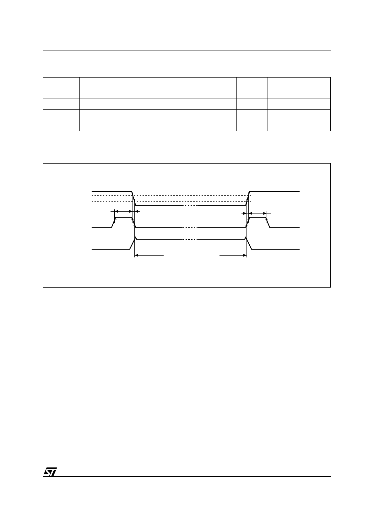
Figure 6. Serial Bus Data Transfer Sequence
DATA LINE
STABLE
DATA VALID
CLOCK
DATA
MK41T56, MKI41T56
START
CONDITION
DATA ALLOWED
Figure 7. Acknowledgement Sequence
START
SCLK FROM
MASTER
DATA OUTPUT
BY TRANSMITTER
DATA OUTPUT
BY RECEIVER
12 89
DATA 1 DATA 2 DATA 8
Figure 8. Bus Timing Requirements Sequence
CHANGE OF
STOP
CONDITION
AI00587
CLOCK PULSE FOR
ACKNOWLEDGEMENT
AI00588
SDA
SCL
tHD:STAtBUF
tR
SP
tHIGH
tLOW
tF
tSU:DAT
tHD:DAT
SR
tHD:STA
tSU:STOtSU:STA
P
AI00589
7/15
Page 8

MK41T56, MKI41T56
WRITE MODE
In this mode the master transmitter transmits to the
MK41T56 slave receiver. Bus protocol is shown in
Figure 10. Following the START condition and
slave address, a logic ’0’ (R/
W = 0) is placed on the
bus and indicates to the addressed device that
word address A
will follow and is to be written to
n
the on-chip address pointer. The data word to be
written to the memory is strobed in next and the
internal address pointer is incremented to the next
memory location within the RAM on the reception
of an acknowledge clock. The MK41T56 slave
receiver will send an acknowledge clock to the
master transmitter after it has received the slave
address and again after it has received the word
address and each data byte (see Figure 9).
READ MODE
In this mode, the master reads the MK41T56 slave
after setting the slave address (see Figure 11).
Following the write mode control bit (R/
the acknowledge bit, the word addr ess A
W = 0) and
is written
n
to the on-chip address pointer. Next the START
condition and slave address are repeated, followed
by the READ mode control bit (R/
W = 1). At this
point, the master transmitter becomes the master
receiver. The data byte which was addressed will
be transmitted and the master receiver will s end an
acknowledge bit to the slave transmitter. The address pointer is only incremented on reception of
an acknowledge bit. The MK41T56 slave transmitter will now place the data by te at address An + 1
on the bus. The master receiver reads and acknow-
Figure 9. Slave Address Location
R/W
ledges the new byte and the address pointer is
incremented to An + 2.
This cycle of reading consecutive addresses will
continue until the master receiver sends a STOP
condition to the slave transmitter.
An alternate READ mode may also be implemented, whereby the master reads the MK41T56
slave without first writing to the (volatile) address
pointer. The first address that is read is the last one
stored in the pointer, see Figure 12.
CLOCK CALIBRATION
The MK41T56 is driven by a quartz controlled
oscillator with a nominal frequency of 32,768 Hz. A
typical MK41T56 is accurate within ± 1 minute per
month at 25°C without calibration. The devices are
tested not to exceed 35 ppm (parts per million)
oscillator frequency error at 25°C, which equates
to about ± 1.53 minutes per month. The oscillation
rate of any crystal changes with temperature ( see
Figure 14).
Most clock chips compens ate for crystal frequency
and temperature shift error wit h c umbersome trim
capacitors. The MK41T56 design, however, employs periodic counter correction. The calibration
circuit adds or subtracts counts from the oscillator
divider circuit at the divide by 256 stage, as shown
in Figure 13. The number of times pulses are
blanked (subtracted, negative calibration) or split
(added, positive calibration) depends upon the
value loaded into the five bit Calibration byte found
in the Control Register. Adding counts speeds the
clock up, subtracting counts slows the clock down.
The Calibration byte occupies the five lower order
bits in the Control register. This byte can be set to
represent any value between 0 and 31 in binary
form. The sixth bit is a sign bit; ’1’ indicates positive
calibration, ’0’ indicates negative calibration. Calibration occurs within a 64 minute cycle. The first
62 minutes in the cycle may, once per minute, have
one second either shortened by 128 or lengthened
by 256 oscillator cycles. If a binary ’1’ is loaded into
the register, only the first 2 minutes in the 64
minutes cycle will be modified; if a binary 6 is
loaded, the first 12 will be affected, and so on.
START A
8/15
SLAVE ADDRESS
0100011
AI00590
Page 9

Figure 10. Write Mode Sequence
MK41T56, MKI41T56
BUS ACTIVITY:
MASTER
BUS ACTIVITY:
START
S
SLAVE
ADDRESS
Figure 11. Read Mode Sequence
BUS ACTIVITY:
MASTER
SDA LINE
BUS ACTIVITY:
START
S
SLAVE
ADDRESS
R/W
WORD
ADDRESS (n)
ACK
R/W
WORD
ADDRESS (n)
ACK
DATA n DATA n+1 DATA n+X
ACK
START
S
ACK
ADDRESS
SLAVE
ACK
R/W
DATA n DATA n+1
ACK
ACK
ACK
STOP
PSDA LINE
ACK
AI00591
ACK
DATA n+X
Figure 12. Alternate Read Mode Sequence
BUS ACTIVITY:
MASTER
BUS ACTIVITY:
START
S
SLAVE
ADDRESS
R/W
DATA n DATA n+1 DATA n+X
ACK
STOP
P
NO ACK
ACK
ACK
ACK
AI00592B
STOP
PSDA LINE
ACK
AI00593
9/15
Page 10

MK41T56, MKI41T56
Figure 13. Clock Calibration
NORMAL
POSITIVE
CALIBRATION
NEGATIVE
CALIBRATION
AI00594B
CLOCK CALIBRATION
(cont’d)
Therefore, each calibration step has the effect of
adding 512 or subtracting 256 oscillator cycles for
every 125,829,120 actual oscillator cycles, that is
+ 4.068 or –2.034 ppm of adjustment pe r calibration step in the calibration register. Assuming that
the oscillator is in fact running at exactly 32,768 Hz,
each of the 31 inc rements in the Calibration byt e
would represent 10.7 seconds per month.
Two methods are available for ascertaining how
much calibration a given MK41T56 may require.
The first involves simply setting the clock, letting it
run for a month and comparing it to a known
accurate reference (like WWV broadcasts). While
that may seem crude, it allows the des igner to give
the end user the ability to calibrate his clock as his
environment may require, even after the final product is packaged in a non-user serviceable enclosure. All the designer has to do is provide a simple
utility that accessed the Calibration byte.
The second approach is better suited to a manufacturing environment, and involves the use of
some test equipment. When the Frequency Test
(FT) bit, the seventh-most significant bit in the
Control Register, is set to a ’1’, and the oscillator is
running at 32,768 Hz, the FT/OUT pin of t he device
will toggle at 512 Hz. Any deviation fro m 512 Hz
indicates the degree and direction of oscillator frequency shift at the test temperature.
For example, a reading of 512.01024 Hz would
indicate a +20 ppm oscillator frequency error, requiring a –10(XX001010) to be loaded into the
Calibration Byte for correction. Note that setting or
changing the Calibration Byte does not affect the
Frequency test output frequency.
OUTPUT DRIVER PIN
When the FT bit is not set, the FT/OUT pin becomes
an output driver that reflects the contents of D7 of
the control register. In other words, when D6 of
location 7 is a zero and D7 of location 7 is a zero
and then the FT/OUT pin will be driven low.
Note:
The FT/OUT pin is open drain whic h requires
an external pull-up resistor.
10/15
Page 11

Figure 14. Crystal Accuracy Across Temperature
ppm
20
0
-20
-40
MK41T56, MKI41T56
∆F
= -0.038 (T - T
-60
-80
-100
0 5 10 15 20 25 30 35 40 45 50 55 60 65 70
F
ppm
2
C
T0 = 25 °C
)2 ± 10%
0
°C
AI02124
11/15
Page 12

MK41T56, MKI41T56
ORDERING INFORMATION SCHEME
Example: MKI41T56 N 00 TR
Operating Temp.
blank 0 to 70°C
I –40 to 85°C
Package
N PSDIP8
0.4mm Frame
S SO8
0.15mm Frame
Speed
00 No Speed Options
Shipping Method for SO
blank Tubes
TR Tape & Reel
For a list of available options or for further information or any aspect of this device, please contact the
STMicroelectronics Sales Office nearest to you.
12/15
Page 13

MK41T56, MKI41T56
PSDIP8 - 8 pin Plastic Skinny DIP, 0.4mm lead frame
Symb
Typ Min Max Typ Min Max
A 4.80 0.189
A1 0.70 – 0.028 –
A2 3.10 3.60 0.122 0.142
B 0.38 0.58 0.015 0.023
B1 1.15 1.65 0.045 0.065
C 0.38 0.52 0.015 0.020
D 9.20 9.90 0.362 0.390
E 7.62 – – 0.300 – –
E1 6.30 7.10 0.248 0.280
e1 2.54 – – 0.100 – –
eA 8.40 – 0.331 –
eB 9.20 0.362
L 3.00 3.80 0.118 0.150
N8 8
mm inches
Drawing is not to scale.
A2
A1AL
B
e1
B1
D
N
C
eA
eB
E1 E
1
PSDIP-a
13/15
Page 14

MK41T56, MKI41T56
SO8 - 8 lead Plastic Small Outline, 150 mils body width
Symb
Typ Min Max Typ Min Max
A 1.35 1.75 0.053 0.069
A1 0.10 0.25 0.004 0.010
B 0.33 0.51 0.013 0.020
C 0.19 0.25 0.007 0.010
D 4.80 5.00 0.189 0.197
E 3.80 4.00 0.150 0.157
e1.27– –0.050– –
H 5.80 6.20 0.228 0.244
h 0.25 0.50 0.010 0.020
L 0.40 0.90 0.016 0.035
α 0° 8° 0° 8°
N8 8
CP 0.10 0.004
mm inches
Drawing is not to scale.
14/15
B
SO-a
h x 45˚
A
C
e
CP
D
N
E
H
1
LA1 α
Page 15

MK41T56, MKI41T56
Information furnished is believed to be accurate a nd rel i abl e. However, STMicroelectronics assumes no responsibility for the consequences
of use of such information nor for any infringement of patents or other rights of third parties which may result from its use. No license is granted
by implication or otherwise under any patent or patent rights of STMicroelectronics. Specifications mentioned in this publication are subject to
change without notice. This publication supersedes and repl aces all information previously supplied. STMicroelectron ics products are not
authorized for use as critical components in life support devices or systems without express written approval of STMicroelectronics.
The ST logo is a registered trademark of STMicroelect roni cs
© 1999 STMicroelectronics - All Rights Reserved
All other names are the property of their respective owners
Australia - Brazil - Canada - China - France - Germany - Italy - Japan - Korea - Malaysia - Malta - Mexico - Morocco - The Netherlands -
Singapore - Spain - Sweden - Switzerland - Taiwan - Thailand - United Kingdom - U.S.A.
STMicroelectronics GROUP OF COMPANIES
http://www.st.com
15/15
 Loading...