

Page 1
MK1491-06
CS5530 Geode™ Clock Source
Description
The MK1491-06 is a low cost, low jitter, high
performance clock synthesizer for National
Semiconductor CS5530 based computer and
portable appliance applications. Using patented
analog Phase-Locked Loop (PLL) techniques,
the device accepts a 14.318 MHz crystal input to
produce multiple output clocks. It provides
selectable PCI local bus and AC97 audio clocks,
24 MHz and 48 MHz clocks for Super I/O and
USB, as well as multiple Reference outputs.
The device has multiple power down modes to
reduce power consumption.
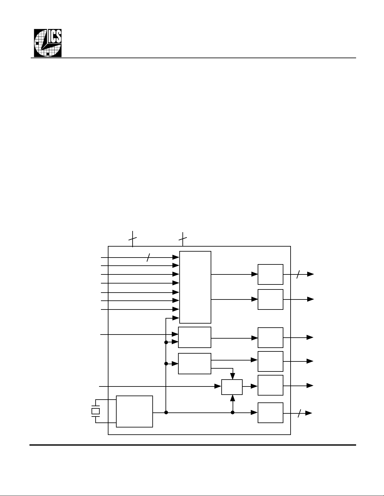
Block Diagram
PCI Frequency Select
Low EMI Enable
PCIF Function Enable
Early PCI Enable
SLOW#
PCISTP#
PWRDWN#
VDD GND
2
Features
• Packaged in 28 pin, 300 mil wide SOIC or in
28 pin, 150 mil wide SSOP
• Provides all critical timing for the National
Semiconductor CS5530 Geode companion chip
• Four PCI clocks
• Selectable PCIF on up to 2 outputs
• Early PCI clock selectability
• Up to 4 Reference clocks
• 48 MHz USB and 24MHz SIO support
• AC97 audio clock
• Multiple power down modes
• Low EMI Enable pin reduces EMI radiation on
PCI clocks (patented)
• 3.3 V ±5% operation
56
3
PCI
EPCI/PCI
PCI
Clocks
Output
Buffers
Output
Buffer
Audio Select
14.3M/24M Select
XI
14.31818 MHz
crystal
XO
MDS 1491-06 F 1 Revision 101700 Printed 11/15/00
Crystal
Oscillator
Audio
Clock
Fixed
Clocks
MUX
Output
Buffer
Output
Buffer
Output
Buffer
Output
Buffers
3
16.934 MHz or
24.576 MHz or
49.152 MHz
48 MHz
14.318 MHz or
24 MHz
14.318 MHz
Integrated Circuit Systems, Inc. • 525 Race Street • San Jose • CA • 95126 • (408)295-9800tel • www.icst.com
Page 2

MK1491-06
CS5530 Geode™ Clock Source
Pin Assignment
VDD
XI
XO
GND
14.3M(TS)
14.3M
GND
14.3M(SEL AUDIO)
VDD
SLOW#
GND
FS
SEL24
VDD
1
2
3
4
5
6
7
8
9
10
11
12
13
14
AC97 AUDIO(PEN)
28
PCI
27
VDD
26
PCI
25
PCI
24
23
GND
22
PCI(EPCI#)
21
48M(LE#)
20
VDD
19
24M/14.3M
18
VDD
17
GND
16
PCISTP#
15
PWRDWN#
24M/14.3M Frequency
Select Table
SEL24 24M/14.3M
0 14.31818 MHz
1 24.0 MHz
PCIF Enable Control
PEN Pin 25 Pin 24
0 PCI PCI
M PCI PCIF
1 PCIF PCIF
PCIF continues to run in PCI STOP
mode. See table on page 4.
PCI Frequency Select Table
TS FS PCI
0 0 Tristate all clocks
0 1 Reserved
M 0 30 MHz
M 1 33.3 MHz
1 0 25 MHz
1 1 37.5 MHz
Early PCI Control Table
EPCI# PCI (Pin 22)
0
1
1 ns early
Normal
EMI Control
AC97 Audio Frequency Select
SEL AUDIO AC97 AUDIO
0 16.9344 MHz
M 24.576 MHz
1 49.152 MHz
LE# PCI Low EMI
0 ON
1 OFF
Spread direction is DOWN..
Pin Descriptions
Pin # Name Type Description
1, 9, 14 VDD P Connect to +3.3V. Must be same voltage on all pins.
2 XI I Crystal connection. Connect to a 14.31818 MHz crystal or input clock.
3 XO O Crystal connection. Connect to a 14.31818 MHz crystal, or leave unconnected for clock.
4, 7, 11, 17, 23 GND P Connect to Ground.
5 14.3M(TS) TI/O 14.318 MHz output. Input control for all clocks per table above.
6 14.3M O 14.318 MHz buffered reference clock output.
8 14.3M(SEL AUDIO) TI/O 14.318 MHz output and audio frequency select input per table above.
10 SLOW# I PCI normal or slow mode select input per table on page 4.
12 FS I Frequency Select for PCI clocks per table above.
13 SEL24 I Fixed frequency select input per table above. Selects frequency on pin 19.
15 PWRDWN# I Power down control; defined in table on page 4.
16 PCISTP# I PCI Stop power down control; defined in table on page 4.
18, 20, 26 VDD P Connect to +3.3V. Must be same voltage on all pins.
19 24M/14.3M O Fixed frequency clock output per table above.
21 48(LE#) I/O Fixed frequency clock output and low EMI (spread spectrum) enable input per table above.
22 PCI(EPCI#) I/O PCI Output clock that can be early. Input control for Early PCI per table above.
24 PCI O PCI Output clock. PCI/PCIF control set by PEN per table above.
25 PCI O PCI Output clock. PCI/PCIF control set by PEN per table above.
27 PCI O PCI Output clock.
28 AC97 AUDIO(PEN) TI/O Audio clock output and PCIF Function Enable per table above.
Key: I = Input, TI = tri-level input, O = Output, P = Power supply connection, (T)I/O = Input on power up, becomes an Output after 10ms.
Weak internal pull-up resistors are present on SEL24, EPCI#, FS, LE#, PCISTP#, and SLOW#. These pins should be tied to VDD or GND,
and not be left floating. Internal resistors on PEN, SEL AUDIO, and TS pull to a mid-level (M).
MDS 1491-06 F 2 Revision 101700 Printed 11/15/00
Integrated Circuit Systems, Inc. • 525 Race Street • San Jose • CA • 95126 • (408)295-9800tel • www.icst.com
Page 3

MK1491-06
ABSOLUTE MAXIMUM RATINGS (note 2)
DC CHARACTERISTICS (VDD = 3.3V unless noted)
AC CHARACTERISTICS (VDD = 3.3V unless noted)
CS5530 Geode™ Clock Source
Electrical Specifications
Parameter Conditions Minimum Typical Maximum Units
Supply voltage, VDD Referenced to GND 7 V
Inputs and Clock Outputs Referenced to GND -0.5 VDD+0.5 V
Ambient Operating Temperature 0 70 °C
Soldering Temperature Max of 10 seconds 260 °C
Storage temperature -65 150 °C
Operating Voltage, VDD 3.1 3.3 3.45 V
Input High Voltage, VIH 2 V
Input Mid-Level Voltage, VIM 1.2 1.4 1.6 V
Input Low Voltage, VIL 0.8 V
Output High Voltage, VOH IOH=-8mA 2.4 V
Output Low Voltage, VOL IOL=8mA 0.4 V
Output High Voltage, VOH IOH=-8mA VDD-0.4 V
Operating Supply Current, IDD No Load, 33.3 MHz 30 mA
Power Down mode Supply Current 15 µΑ
Short Circuit Current, single output driver VDD=3.3V ±60 mA
Input Capacitance 7 pF
Input Frequency 14.31818 MHz
Output Clock Rise Time 0.8 to 2.0V 1.5 ns
Output Clock Fall Time 2.0 to 0.8V 1.5 ns
Output Clock Duty Cycle, all MHz clocks At 1.5V 45 49 to 51 55 %
PCI Output to Output Skew Rising edges at 1.5V 500 ps
Skew of EPCI with respect to PCI 1 ns
Cycle to Cycle Jitter, PCI clocks 250 ps
EMI reduction, peaks of 5th - 19th odd harmonics 33.3 MHz PCI clock 6 11 dB
Power up time, PWRDWN# high to all clocks stable 8 20 ms
Power on time, applied VDD to all clocks stable 12 25 ms
Note: Stresses beyond those listed under Absolute Maximum Ratings could cause permanent damage to the device. Prolonged exposure to levels above the
operating limits but below the Absolute Maximums may affect device reliability.
MDS 1491-06 F 3 Revision 101700 Printed 11/15/00
Integrated Circuit Systems, Inc. • 525 Race Street • San Jose • CA • 95126 • (408)295-9800tel • www.icst.com
Page 4

MK1491-06
resistors are the normal output
termination resistors. The 10kΩ resistor pulls low to generate a logic
zero. Weak internal pull-up resistors are present on SEL24, EPCI#, FS,
LE#, PCISTP#, and SLOW#. These pins should be connected directly to
VDD or GND if not under active control. Internal resistors on PEN, SEL
AUDIO, and TS pull to a mid-level (M).
CS5530 Geode™ Clock Source
Power Down Control Table
PCISTP# PWRDWN# SLOW#
X 0 X
0 1 X
1 1 X
Key: 1 = connected to VDD, 0 = connected to ground, X = any valid logic level, Combination Input/Outputs should be connected to VDD or
Ground through a 10 kΩ resistor as shown below.
MODE
Power Down
PCI STOP
ON
Power-On Default Conditions
Input Pin# Function Default Condition
5 TS M All outputs enabled.
8 SEL AUDIO M Audio clock (pin 28) set to 24.576 MHz
10 SLOW# 1 PCI clocks set to 33.3 MHz. Refer to Power Down Control Table above.
12 FS 1 PCI frequency = 33.3 MHz.
13 SEL24 1 24M/14.3M (pin 19) set to 24 MHz.
15 PWRDWN# 1 All clocks running.
16 PCISTP# 1 PCI clocks running.
21 LE# 1 Low EMI function OFF
22 EPCI# 1 Pin 22 set to normal PCI signal (not early).
28 PEN M PCI (pin 25) set to PCI clock (33.33 MHz). PCI (pin 24) set to PCIF clock (33.33 MHz).
PCI PCIF 24/14.3 14.3 DESCRIPTION
LOW LOW LOW LOW All outputs low. PLLs and Oscillator off.
LOW ON ON ON PCI clocks synchronously enter and leave low state.
ON ON ON ON All Clocks On.
External Components
The MK1491-06 requires some inexpensive external components for proper operation. Decoupling capacitors of 0.1µF should be
connected on each VDD pin to ground, as close to the MK1491-06 as possible. A series termination resistor of 33Ω may be used for
each clock output. See the discussion below for other external resistors required for proper I/O operation. The 14.3 MHz oscillator
has internal caps that provide the proper load for a parallel resonant crystal with CL=18 pF. For tuning with other values of CL, the
formula 2*(CL-18) gives the value of each capacitor that should be connected between X1 and ground and X2 and ground.
I/O Structure
The MK1491-06 provides more functionality in a 28 pin package by using
a unique I/O technique. The device checks the status of all I/O pins
during power-up and at exit from the Power Down state. This status
(pulled high, low, or mid-level) then determines the frequency selections
and power down modes (see the tables on pages 2 and 4). Within 10ms
after power up, the inputs change to outputs and the clocks start up. In the
diagrams to the right, the 33Ω
MDS 1491-06 F 4 Revision 101700 Printed 11/15/00
Integrated Circuit Systems, Inc. • 525 Race Street • San Jose • CA • 95126 • (408)295-9800tel • www.icst.com
33Ω
I/O
to load*
For select
= 0 (low)
10kΩ
Don’t stuff for
“1” selection
*Note: Do not use a TTL load. This will
overcome the 10 kΩ pulldown and force the
input to a logic 1.
Page 5

CS5530 Geode™ Clock Source
Inches
Millimeters
Package Outline and Package Dimensions
(For current dimensional specifications, see JEDEC Publication No. 95.)
28 pin SOIC
Symbol Min Max Min Max
A -- 0.104 -- 2.65
A1 0.0040 -- 0.10 --
B 0.013 0.020 0.33 0.51
E H
INDEX
AREA
1 2
h x 45°
D
C 0.007 0.013 0.18 0.33
D 0.697 0.724 17.70 18.39
E 0.291 0.299 7.40 7.60
e
H 0.394 0.419 10.01 10.64
h 0.01 0.029 0.25 0.74
L 0.016 0.050 0.41 1.27
MK1491-06
A1 C
e
B
A
L
MDS 1491-06 F 5 Revision 101700 Printed 11/15/00
Integrated Circuit Systems, Inc. • 525 Race Street • San Jose • CA • 95126 • (408)295-9800tel • www.icst.com
Page 6

CS5530 Geode™ Clock Source
Inches
Millimeters
Package Outline and Package Dimensions
(For current dimensional specifications, see JEDEC Publication No. 95.)
28 pin SSOP
Symbol Min Max Min Max
A 0.053 0.069 1.35 1.75
A1 0.004 0.010 0.10 0.25
b 0.008 0.012 0.20 0.30
c 0.007 0.010 0.19 0.25
D 0.386 0.394 9.80 10.01
e
E 0.228 0.244 5.79 6.20
E1 0.150 0.157 3.81 3.99
L 0.016 0.050 0.41 1.27
INDEX
AREA
E1 E
1 2
MK1491-06
D
A
A1 c
e
b
L
Ordering Information
Part/Order Number Marking Low EMI Feature Package Temperature
MK1491-06R MK1491-06R Yes 28 pin SSOP 0 to 70°C
MK1491-06RTR MK1491-06R Yes Add Tape & Reel 0 to 70°C
MK1491-06S MK1491-06S Yes 28 pin SOIC 0 to 70°C
MK1491-06STR MK1491-06S Yes Add Tape & Reel 0 to 70°C
While the information presented herein has been checked for both accuracy and reliability, ICS assumes no responsibility for either its use or for the infringement of any patents
or other rights of third parties, which would result from its use. No other circuits, patents, or licenses are implied. This product is intended for use in normal commercial
applications. Any other applications such as those requiring extended temperature range, high reliability, or other extraordinary environmental requirements are not
recommended without additional processing by ICS. ICS reserves the right to change any circuitry or specifications without notice. ICS does not authorize or warrant any ICS
product for use in life support devices or critical medical instruments.
Geode is a trademark of National Semiconductor Corporation
MDS 1491-06 F 6 Revision 101700 Printed 11/15/00
Integrated Circuit Systems, Inc. • 525 Race Street • San Jose • CA • 95126 • (408)295-9800tel • www.icst.com
 Loading...