

Page 1
OPL3, OPL4 + Codec Clock Source
Description Features
MK1418/MK1420
The MK1418 and MK1420 are the ideal way to
generate clocks for new sound cards. The MK1420
provides clocks for Analog Devices’ AD1848,
Crystal Semiconductor’s CS4231, and Yamaha’s
OPL3L, OPL3LS, and OPL4. The MK1420 uses
either a 14.318 MHz crystal, or a 14.318 MHz bus
clock input to synthesize the clocks required to
drive the codec, and the 33.868 MHz required for
the FM or wavetable music synthesizer. The chips
are ideal for add-in sound cards and motherboards
with integrated sound. In an 8 pin SOIC, the
MK1420 can save component count, board space,
and cost over surface mount crystals, and increase
reliability by eliminating three or four mechanical
devices from the board.
MicroClock offers many other parts with stereo
codec support. The MK1430 has 5 output clocks,
the MK1448 has 7, the MK1444 has eight
including DSP clocks, and the MK1450/1 offers
Pentium™ and SCSI support, plus the stereo
codec clocks.
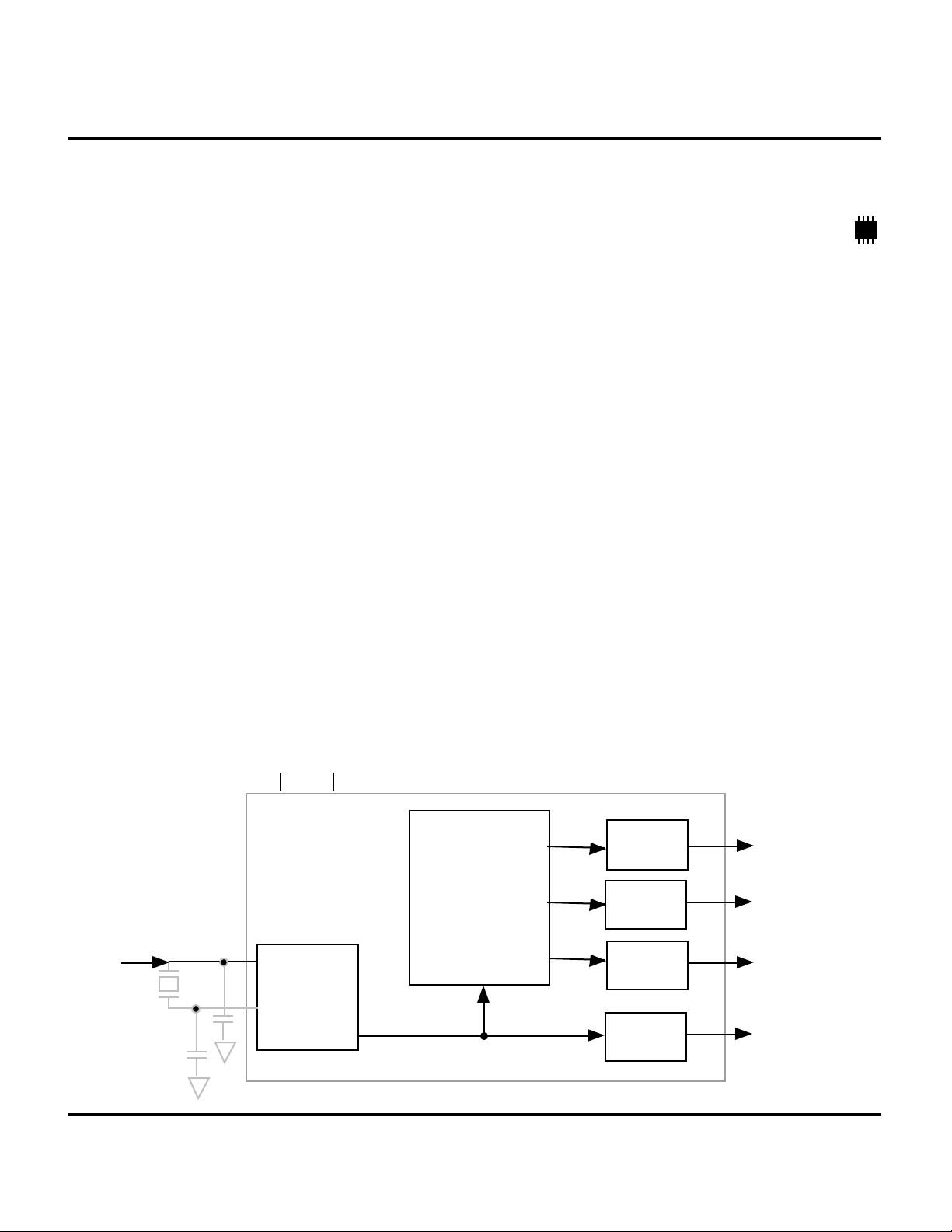
Block Diagram
VDD GND
• Packaged in 8 pin SOIC
• Input crystal or clock frequency of 14.318 MHz
• MK1418 is clock input only
• MK1420 output clock frequencies of 16.934MHz,
24.576 MHz, 33.868 MHz, and 14.318 MHz
• Advanced, low power CMOS process
• Lowest jitter in industry for best audio
performance
• Insensitive to input clock duty cycle
• 50% (typ) 14.318 MHz duty cycle with crystal
AC Coupling/Portable Applications
For applications in portable computers, it is possible
to drive the input clock with a 3.3V, 14.318MHz
clock by a.c. coupling using a 0.01µF capacitor
connected in series to the CLKIN pin. But the
operating VDD on pin 2 must be 5V±10%. This
technique is also effective if the input clock doesn’t
meet the VIH and VIL specifications on page 3.
Additional Clocks or Features
If more than these four output clocks or features
such as power down are needed, MicroClock has
many other products in development. Consult
MicroClock for your specific needs.
Output
Buffer
Clock Synthesis
14.318 MHz
crystal or clock
X1
Crystal
Oscillator
X2
MDS 1418/20 A 1 Revision 013098 Printed 11/15/00
MicroClock Division of ICS•1271 Parkmoor Ave.•San Jose•CA•95126•(408)295-9800tel•(408)295-9818fax
Circuitry
Output
Buffer
Output
Buffer
Output
Buffer
16.934 MHz
24.576 MHz
33.868 MHz
(MK1420 only)
14.318 MHz
(MK1420 only)
Page 2
Pin Assignments
MK1418
ICLK
VDD
GND
16.9M
1 8
2
3
4
MK1420
MK1418/MK1420
OPL3, OPL4 + Codec Clock Source
Suggested Layout
for MK1420
GND
7
VDD
6
GND
5
24.6M
V
0.1µF
clock only
G
14.318 MHz
crystal
Pin 1
2
3
8
7
6
4
5
14.3MHz out
33Ω (optional)
33.9MHz out
33Ω (optional)
X1
VDD
GND
16.9M
1 8
2
3
4
X2
7
14.3M
6
33.9M
5
24.6M
33Ω (optional)
16.9MHz out
33Ω (optional)
24.6MHz out
Pin Descriptions for MK1420
Number Name Type Description
1 X1 I Crystal Connection. Connect to a 14.318 MHz crystal or clock.
2 VDD P Connect to +5V.
3 GND P Connect to ground.
4 16.9M O 16.9344 MHz clock output for stereo codec.
5 24.6M O 24.576 MHz clock output for stereo codec.
6 33.9M O 33.868 MHz clock output for OPL4.
7 14.3M O 14.318 MHz clock buffered output for OPL3 or PCMCIA controller.
8 X2 O Crystal Connection to a 14.318 MHz crystal, or leave unconnected for clock input.
Key: I = Input, O = output, P = power supply connection
External Components/Crystal Selection
A minimum number of external components are required for proper oscillation. For a crystal input, one
22pF load capacitor should be connected to each of the X1 and X2 pins and ground, and a parallel
resonant 14.318 MHz, 16pF load, crystal is recommended. Values near these are acceptable, as is a series
resonant crystal, but either will result in frequencies which are slightly (up to 0.06%) different from the
ideal. For a clock input, connect to X1 and leave X2 unconnected. A decoupling capacitor of 0.1µF should
be connected between VDD and GND, and 33Ω terminating resistors may be used on the clock outputs.
These terminating resistors are unnecessary for clock traces less than 1” (25mm).
MDS 1418/20 A 2 Revision 013098 Printed 11/15/00
MicroClock Division of ICS•1271 Parkmoor Ave.•San Jose•CA•95126•(408)295-9800tel•(408)295-9818fax
Page 3

MK1418/MK1420
ABSOLUTE MAXIMUM RATINGS (note 1)
DC CHARACTERISTICS (at 5.0V unless otherwise noted)
OPL3, OPL4 + Codec Clock Source
Electrical Specifications
Parameter Conditions Minimum Typical Maximum Units
Supply Voltage, VDD Referenced to GND 7 V
Inputs Referenced to GND -0.5 VDD+.5V V
Clock Outputs Referenced to GND -0.5 VDD+.5V V
Ambient Operating Temperature 0 70 °C
Soldering Temperature Max of 20 seconds 260 °C
Storage temperature -65 150 °C
Operating Voltage, VDD 4.5 5.5 V
Input High Voltage, VIH 3.5 2.5 V
Input Low Voltage, VIL 2.5 1.5 V
Output High Voltage, VOH IOH=-4mA VDD-0.4 V
Output High Voltage, VOH IOH=-25mA 2.4 V
Output Low Voltage, VOL IOL=25mA 0.4 V
Operating Supply Current, IDD No Load 18 mA
Input Capacitance 7 pF
Actual Mean Frequency versus Target Outputs ±0.2 %
AC CHARACTERISTICS
Input Clock or Crystal Frequency 14.31818 MHz
Input Clock Duty Cycle, 14.318MHz Time above 2.5V 20 80 %
Output Clock Rise Time 0.8 to 2.0V 1.5 ns
Output Clock Fall Time 2.0 to 0.8V 1.5 ns
Output Clock Duty Cycle, 24.576MHz Time above 1.5V 40 45 60 %
Output Clock Duty Cycle, 16.9344 MHz Time above 1.5V 45 50 55 %
Output Clock Duty Cycle, 33.868MHz Time above 1.5V 45 50 55 %
Output Clock Duty Cycle, 14.318 MHz, Note 3 Time above 1.5V 45 50 55 %
Absolute Clock Period Jitter, except 14.3 Pins 4, 5, 6 only -400 200 400 ps
One Sigma Clock Period Jitter, except 14.3 Pins 4, 5, 6 only 60 ps
Notes:
1. Stresses beyond those listed under Absolute Maximum Ratings could cause permanent damage to the device. Prolonged exposure
to levels above the operating limits but below the Absolute Maximums may affect device reliability.
2. Typical values are at 25°C.
3. If crystal is used as input with CL = 16pf. If a clock is used as input, the duty cycle of the 14.318MHz output will be the same as the
input clock.
MDS 1418/20 A 3 Revision 013098 Printed 11/15/00
MicroClock Division of ICS•1271 Parkmoor Ave.•San Jose•CA•95126•(408)295-9800tel•(408)295-9818fax
Page 4

Package Outline and Package Dimensions
Inches
Millimeters
8 pin SOIC
E H
Pin 1
h x 45°
c
L
Q
D
e
b
MK1418/MK1420
OPL3, OPL4 + Codec Clock Source
Symbol Min Max Min Max
A 0.055 0.061 1.397 1.5494
b 0.013 0.019 0.330 0.483
D 0.185 0.200 4.699 5.080
E 0.150 0.160 3.810 4.064
H 0.225 0.245 5.715 6.223
e
h 0.015 0.381
Q 0.004 0.01 0.102 0.254
L 0.016 0.035 0.406 0.889
A
Ordering Information
Part/Order Number Marking Package Temperature
MK1418S MK1418S 8 pin SOIC 0-70°C
MK1418STR MK1418S Add tape and reel 0-70°C
MK1420S MK1420S 8 pin SOIC 0-70°C
MK1420STR MK1420S Add tape and reel 0-70°C
While the information presented herein has been checked for both accuracy and reliability, MicroClock Incorporated assumes no responsibility for either its use or for the
infringement of any patents or other rights of third parties, which would result from its use. No other circuits, patents, or licenses are implied. This product is intended for use in
normal commercial applications. Any other applications such as those requiring extended temperature range, high reliability, or other extraordinary environmental requirements
are not recommended without additional processing by MicroClock. MicroClock reserves the right to change any circuitry or specifications without notice. MicroClock does not
authorize or warrant any MicroClock product for use in life support devices or critical medical instruments.
1201BO.7
MDS 1418/20 A 4 Revision 013098 Printed 11/15/00
MicroClock Division of ICS•1271 Parkmoor Ave.•San Jose•CA•95126•(408)295-9800tel•(408)295-9818fax
 Loading...