

Page 1
1
Motorola Bipolar Power Transistor Device Data
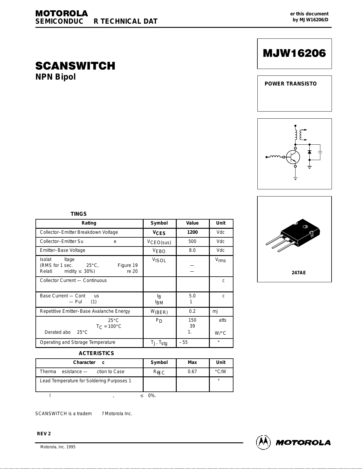
SCANSWITCH
NPN Bipolar Power Deflection Transistors
For High and Very High Resolution CRT Monitors
The MJF16206 and the MJW16206 are state–of–the–art SWITCHMODE bipolar
power transistors. They are specifically designed for use in horizontal deflection
circuits for high and very high resolution, monochrome and color CRT monitors.
• 1200 Volt V
CES
Breakdown Capability
• Typical Dynamic Desaturation Specified (New Turn–Off Characteristic)
• Maximum Repetitive Emitter–Base Avalanche Energy Specified (Industry First)
• High Current Capability: Performance Specified at 6.5 Amps
Continuous Rating — 12 Amps Max
Pulsed Rating — 15 Amps Max
• Isolated MJF16206 is UL Recognized
• Fast Switching: 100 ns Inductive Fall Time (Typ)
1000 ns Inductive Storage Time (Typ)
• Low Saturation Voltage
0.25 Volts (Typ) at 6.5 Amps Collector Current
• High Emitter–Base Breakdown Capability For High Voltage Off Drive Circuits —
8.0 V (Min)
MAXIMUM RATINGS
Rating
Symbol
Value
ÎÎÎ
ÎÎÎ
ÎÎÎ
Unit
Collector–Emitter Breakdown Voltage
V
CES
1200
ÎÎÎ
ÎÎÎ
ÎÎÎ
Vdc
Collector–Emitter Sustaining Voltage
V
CEO(sus)
500
ÎÎÎ
ÎÎÎ
ÎÎÎ
Vdc
Emitter–Base Voltage
V
EBO
8.0
ÎÎÎ
ÎÎÎ
ÎÎÎ
Vdc
Isolation Voltage
(RMS for 1 sec., TA = 25_C, Figure 19
Relative Humidity v 30%) Figure 20
V
ISOL
—
—
ÎÎÎ
ÎÎÎ
ÎÎÎ
ÎÎÎ
V
rms
Collector Current — Continuous
Collector Current — Pulsed (1)
I
C
I
CM
12
15
ÎÎÎ
ÎÎÎ
ÎÎÎ
ÎÎÎ
Adc
Base Current — Continuous
Base Current — Pulsed (1)
I
B
I
BM
5.0
10
ÎÎÎ
ÎÎÎ
ÎÎÎ
Adc
Repetitive Emitter–Base Avalanche Energy
W
(BER)
0.2
ÎÎÎ
ÎÎÎ
ÎÎÎ
mjoules
Total Power Dissipation @ TC = 25_C
Total Power Dissipation @ TC = 100_C
Derated above 25_C
P
D
150
39
1.49
ÎÎÎ
ÎÎÎ
ÎÎÎ
ÎÎÎ
ÎÎÎ
Watts
W/_C
Operating and Storage Temperature
TJ, T
stg
–55 to +150
ÎÎÎ
ÎÎÎ
ÎÎÎ
_
C
THERMAL CHARACTERISTICS
Characteristic
Symbol
Max
ÎÎÎ
ÎÎÎ
ÎÎÎ
Unit
Thermal Resistance — Junction to Case
R
θJC
0.67
ÎÎÎ
ÎÎÎ
ÎÎÎ
_
C/W
Lead Temperature for Soldering Purposes 1/8″
from the Case for 5 seconds
T
L
260
ÎÎÎ
ÎÎÎ
ÎÎÎ
ÎÎÎ
_
C
(1) Pulse Test: Pulse Width = 5.0 ms, Duty Cycle v 10%.
SCANSWITCH is a trademark of Motorola Inc.
MOTOROLA
SEMICONDUCTOR TECHNICAL DATA
Order this document
by MJW16206/D
Motorola, Inc. 1995
MJW16206
POWER TRANSISTORS
12 AMPERES
1200 VOLTS — V
CES
50 and 150 WATTS
CASE 340F–02
TO–247AE
REV 2
Page 2
MJW16206
2
Motorola Bipolar Power Transistor Device Data
ELECTRICAL CHARACTERISTICS (T
C
= 25_C unless otherwise noted)
Characteristic
Symbol
Min
Typ
Max
ÎÎÎ
ÎÎÎ
ÎÎÎ
Unit
OFF CHARACTERISTICS (1)
Collector Cutoff Current
(VCE = 1200 Vdc, VBE = 0 V)
(VCE = 850 Vdc, VBE = 0 V)
I
CES
—
—
—
—
250
25
ÎÎÎ
ÎÎÎ
ÎÎÎ
ÎÎÎ
ÎÎÎ
µAdc
Emitter–Base Leakage
(VEB = 8.0 Vdc, IC = 0)
I
EBO
—
—
25
ÎÎÎ
ÎÎÎ
ÎÎÎ
µAdc
Collector–Emitter Sustaining Voltage (Figure 10)
(IC = 10 mAdc, IB = 0)
V
CEO(sus)
500
—
—
ÎÎÎ
ÎÎÎ
ÎÎÎ
ÎÎÎ
Vdc
Emitter–Base Breakdown Voltage
(IE = 1.0 mA, IC = 0)
V
(BR)EBO
8.0
11
—
ÎÎÎ
ÎÎÎ
ÎÎÎ
ÎÎÎ
Vdc
ON CHARACTERISTICS (1)
Collector–Emitter Saturation Voltage
(IC = 3.0 Adc, IB = 400 mAdc)
(IC = 6.5 Adc, IB = 1.5 Adc)
V
CE(sat)
—
—
0.15
0.25
1.0
1.0
ÎÎÎ
ÎÎÎ
ÎÎÎ
ÎÎÎ
Vdc
Base–Emitter Saturation Voltage
(IC = 6.5 Adc, IB = 1.5 Adc)
V
BE(sat)
—
0.9
1.5
ÎÎÎ
ÎÎÎ
ÎÎÎ
ÎÎÎ
Vdc
DC Current Gain
(IC = 1.0 Adc, VCE = 5.0 Vdc)
(IC = 10 Adc, VCE = 5.0 Vdc)
(IC = 12 Adc, VCE = 5.0 Vdc)
h
FE
—
5.0
3.0
24
8.0
6.0
—
13
—
ÎÎÎ
ÎÎÎ
ÎÎÎ
ÎÎÎ
ÎÎÎ
—
DYNAMIC CHARACTERISTICS
Dynamic Desaturation Interval (Figure 15)
(IC = 6.5 Adc, IB = 1.5 Adc, LB = 0.5 µH)
t
ds
—
250
—
ÎÎÎ
ÎÎÎ
ÎÎÎ
ÎÎÎ
ns
Emitter–Base Avalanche Turn–off Energy (Figure 15)
(t = 500 ns, RBE = 22 Ω)
EB
(off)
—
30
—
ÎÎÎ
ÎÎÎ
ÎÎÎ
µjoules
Output Capacitance
(VCE = 10 Vdc, IE = 0, f
test
= 100 kHz)
C
ob
—
180
350
ÎÎÎ
ÎÎÎ
ÎÎÎ
ÎÎÎ
pF
Gain Bandwidth Product
(VCE = 10 Vdc, IC = 0.5 A, f
test
= 1.0 MHz)
f
T
—
3.0
—
ÎÎÎ
ÎÎÎ
ÎÎÎ
ÎÎÎ
MHz
Collector–Heatsink Capacitance — MJF16206 Isolated Package
(Mounted on a 1″ x 2″ x 1/16″ Copper Heatsink,
VCE = 0, f
test
= 100 kHz)
C
c–hs
—
17
—
ÎÎÎ
ÎÎÎ
ÎÎÎ
ÎÎÎ
pF
SWITCHING CHARACTERISTICS
Inductive Load (Figure 15) (IC = 6.5 A, IB = 1.5 A)
Storage
Fall Time
t
sv
t
fi
—
—
1000
100
2250
250
ÎÎÎ
ÎÎÎ
ÎÎÎ
ÎÎÎ
ns
(1) Pulse Test: Pulse Width = 300 µs, Duty Cycle v 2.0%.
Page 3
MJW16206
3
Motorola Bipolar Power Transistor Device Data
V
CE
, COLLECTOR–EMITTER VOLTAGE (VOLTS)
V
BE
, BASE–EMITTER VOLTAGE (VOLTS)
V
CE
, COLLECTOR–EMITTER VOLTAGE (VOLTS)
1
0.70.3
Figure 1. Typical DC Current Gain
IC, COLLECTOR CURRENT (AMPS)
0.2 2 10
100
h
FE
, DC CURRENT GAIN
1 53
30
7
0.5
TJ = 100°C
25°C
–55°C
7
10
3
1
50
VCE = 5 V
IC, COLLECTOR CURRENT (AMPS)
Figure 2. Typical Collector–Emitter
Saturation Voltage
0.5
3
0.2
5
0.05
1
0.1
0.07
0.3
2
0.7
0.5 32 50.7 1
10 20
TJ = 25°C
TJ = 100
°
C
IC/IB1 = 10
0.3
7
10
70
Figure 3. Typical Collector Saturation Region
IB, BASE CURRENT (AMPS)
0.7
0.1
5
0.3
8 A
0.05 2
4 A 6.5 AIC = 2 A
0.07 0.1
0.2 0.5
5
Figure 4. Typical Base–Emitter
Saturation Voltage
0.30.2 0.5
5
0.7
0.1
0.7 201 10
10
2
TJ = 25°C
2 3 5 7
IC, COLLECTOR CURRENT (AMPS)
TC = 25°C
f = 1 MHz
0.3
Figure 5. Typical Capacitance
10K
VR, REVERSE VOLTAGE (VOLTS)
C
ib
0.1
1K
100
10
1 10 100 1K
2K
200
20
3K
300
5K
500
50
0.3 2 30 300200.5 5 50 500
f
T
, TRANSITION FREQUENCY (MHz)
IC, COLLECTOR CURRENT (AMPS)
Figure 6. Typical Transition Frequency
f
(test)
= 1 MHz
TC = 25
°
C
VCE = 10 V
0.1 0.3 0.7 2 5 107
10
0.7
0.2
3
0.1
0.5
5
2
0.5
0.07
0.2
3
7
2
1
3
IC/IB1 = 5 to 10
7
1
0.2
3
0.5
30
0.2 3 200
1
0.3
7
20
5
2
0.3 20
0.7
5
0.2
10 A
TJ = 25°C
TJ = 100
°
C
0.2 0.5 1 3
7K
700
70
7
C, CAPACITANCE (pF)
C
ob
Page 4

MJW16206
4
Motorola Bipolar Power Transistor Device Data
I
C
, COLLECTOR CURRENT (AMPS)
VCE, COLLECTOR–EMITTER VOLTAGE (VOLTS)
Figure 7. Maximum Forward Biased
Safe Operating Area
2
10
1
0.02
500
WIREBOND LIMIT
THERMAL LIMIT
SECONDARY BREAKDOWN
LIMIT
I
C
, COLLECTOR CURRENT (AMPS)
0.1
1K20 300
3
0.3
0.2
dc
5 ms
10 µs
2
5
0.5
50
0
400 1.2K
IC/IB1 ≥ 5
TJ
≤
100°C
V
BE(off)
= 5 V
0
VCE, COLLECTOR–EMITTER VOLTAGE (VOLTS)
800
0 V
Figure 8. Maximum Reverse Bias
Safe Operating Area
12
20
8
4
600 1K
0.03
30
0.05
20
1005 10 20030
MJW16206
16
1 3
II*
100
ns
*REGION II — EXPANDED FBSOA USING
MUR8100E, ULTRAFAST RECTIFIER (SEE FIGURE 12)
200
2 V
SAFE OPERATING AREA INFORMATION
FORWARD BIAS
There are two limitations on the power handling ability of a
transistor: average junction temperature and second breakdown. Safe operating area curves indicate IC – VCE limits of
the transistor that must be observed for reliable operation;
i.e., the transistor must not be subjected to greater dissipation than the curves indicate.
The data of Figure 7 is based on TC = 25_C; T
J(pk)
is
variable depending on power level. Second breakdown pulse
limits are valid for duty cycles to 10% but must be derated
when TC ≥ 25_C. Second breakdown limitations do not derate the same as thermal limitations. Allowable current at the
voltages shown on Figure 7 may be found at any case temperature by using the appropriate curve on Figure 9.
At high case temperatures, thermal limitations will reduce
the power that can be handled to values less than the limitations imposed by second breakdown.
TC, CASE TEMPERATURE (°C)
0
50 125 150
60
POWER RATING FACTOR (%)
SECOND BREAKDOWN
DERATING
100
80
40
20
75 100
THERMAL
DERATING
25
Figure 9. Power Derating
10
70
90
50
30
REVERSE BIAS
Inductive loads, in most cases, require the emitter–to–
base junction be reversed biased because high voltage and
high current must be sustained simultaneously during turn–
off. Under these conditions, the collector voltage must be
held to a safe level at or below a specific value of collector
current. This can be accomplished by several means such as
active clamping, RC snubbing, load line shaping, etc. The
safe level for these devices is specified as Reverse Biased
Safe Operating Area and represents t he voltage–current
condition allowable during reverse biased turn–off. This rating is verified under clamped conditions so that the device is
never subjected to an avalanche mode. Figure 8 gives the
RBSOA characteristics.
Page 5

MJW16206
5
Motorola Bipolar Power Transistor Device Data
H.P. 214
OR EQUIV.
P.G.
0
≈
–35 V
50
500
1
µ
F
100
–V
2N5337
2N6191
+V
≈
11 V
100
0.02
µ
F
20
10
µ
F
0.02
µ
F
+ –
R
B1
R
B2
A A
50
T
1
+V
0 V
–V
*I
B
*I
C
T.U.T.
L
MR856
V
clamp
V
CC
I
C
V
CE
I
B
I
B1
I
B2
I
C(pk)
V
CE(pk)
T1[
L
coil(ICpk
)
V
CC
Note: Adjust –V to obtain desired V
BE(off)
at Point A.
T1 adjusted to obtain I
C(pk)
V
(BR)CEO
L = 10 mH
RB2 = ∞
VCC = 20 Volts
RBSOA
L = 200 µH
RB2 = 0
VCC = 20 Volts
RB1 selected for desired I
B1
*Tektronix P–6042 or Equivalent
Figure 10. RBSOA/V
(BR)CEO(sus)
Test Circuit
+
–
t, TIME (ms)
0.01
1 100.1
1
0.2
0.1
0.05
r(t), TRANSIENT THERMAL
R
θ
JC
(t) = r(t) R
θ
JC
R
θ
JC
= 0.67
°
C/W MAX
D CURVES APPLY FOR POWER
PULSE TRAIN SHOWN
READ TIME AT t
1
T
J(pk)
– TC = P
(pk)
R
θ
JC
(t)
P
(pk)
t
1
t
2
DUTY CYCLE, D = t1/t
2
SINGLE PULSE
RESISTANCE (NORMALIZED)
Figure 11. Thermal Response
0.5
D = 0.5
100 1K 10K
0.2
0.1
Figure 12. Switching Safe Operating Area
+15
1
µ
F
100
Ω
150
Ω
+10
50
Ω
500 µF
V
Off
150
Ω
MJE210
MUR105
MTP8P10
MPF930
MPF930
100
µ
F
10
µ
F
MUR8100
VCE (1000 V MAX)
10 mH
T.U.T.
R
B2
R
B1
MUR1100
MUR105
MTP12N10
MTP8P10
Note: Test Circuit for Ultrafast FBSOA
Note: RB2 = 0 and V
Off
= –5 Volts
1 µF
Page 6

MJW16206
6
Motorola Bipolar Power Transistor Device Data
DYNAMIC DESATURATION
DYNAMIC DESATURATION
The SCANSWITCH series of bipolar power transistors are
specifically designed to meet the unique requirements of horizontal deflection circuits in computer monitor applications.
Historically, deflection transistor design was focused on minimizing collector current fall time. While fall time is a valid
figure of merit, a more important indicator of circuit performance as scan rates are increased is a new characteristic,
“dynamic desaturation.” In order to assure a linear collector
current ramp, the output transistor must remain in hard saturation during storage time and exhibit a rapid turn–off transition. A sluggish transition results in serious consequences.
As the saturation voltage of the output transistor increases,
the voltage across the yoke drops. Roll off in the collector
current ramp results in improper beam deflection and distortion of the image at the right edge of the screen. Design
changes have been made in the structure of the SCANSWITCH series of devices which minimize the dynamic desaturation interval. Dynamic desaturation has been defined in
terms of the time required for the VCE to rise from 1.0 to
5.0 volts (Figures 13 and 14) and typical performance at optimized drive conditions has been specified. Optimization of
device structure results in a linear collector Current ramp, excellent turn–off switching performance, and significantly lower overall power dissipation.
Figure 13. Deflection Simulator Switching
Waveforms From Circuit in Figure 15
I
C
0% I
B
V
CE
t
sv
VCE = 20 V
t
fi
10% I
C(pk)
Figure 14. Definition of Dynamic
Desaturation Measurement
TIME (ns)
V
CE
DYNAMIC DESATURATION TIME
IS MEASURED FROM VCE = 1 V
TO VCE = 5 V
t
ds
1
4
COLLECTOR-EMITTER VOLTAGE (VOLTS)
5
0
3
2
0
0
90% I
C(pk)
Page 7

MJW16206
7
Motorola Bipolar Power Transistor Device Data
EMITTER–BASE TURN–OFF ENERGY
Typical techniques for driving horizontal outputs rely on a
pulse transformer to supply forward base current, and a
turn–off network that includes a series base inductor to limit
the rate of transition from forward to reverse drive. An alternate d rive scheme h as been used t o characterize the
SCANSWITCH series of devices (see Figure 15). This circuit
produces a ramp of base drive, eliminating the heavy overdrive at the beginning of the collector current ramp and
underdrive just prior to turnoff produced by typical drive strategies. This high performance drive has two additional impor-
tant advantages. First, the configuration of T1 allows LB to be
placed outside the path of forward base current making it unnecessary to expend energy to reverse current flow as in a
series base inductor. Second, there is no base resistor to limit forward base current and hence no power loss associated
with setting the value of the forward base current. The process of generating the ramp stores rather than dissipates energy. Tailoring the amount of e nergy stored in T1 to the
amount of energy , EB
(off)
, that is required to turn–off the output transistor results in essentially lossless operation. [Note:
B+ and the primary inductance of T1 (LP) are chosen such
that 1/2 LP I
b
2
= EB
(off)
].
+24 V
C1
100
µ
F
+
U2
MC7812
V
I
V
O
R13
1K
R3
250
7
V
CC
OUT
R12
470
1 W
GND
R14
150
C7
110 pF
Q2
MJ11016
(IB)
R16
430
R1
1K
R51K(IC)
Q5
MJ11016
C6
100
µ
F
+
L
Y
C
Y
V
CE
R4
22
D2
SCANSWITCH
DAMPER
DIODE
L
B
T
1
D1
MUR110
U1
MC1391P
6
1
2
8
R6
1K
OSC
GND
%
C4
0.005
R7
2.7K
R8
9.1KR9470
C2
10
µ
F
+
MDC1000A
Q6
2N5401
C3
10
µ
F
+
3.9 V
Q3
MTP3055E
R17
120
R15
10K
C5
0.1
Q4 SCANSWITCH
HORIZ OUTPUT
TRANSISTOR
Figure 15. High Resolution Deflection Application Simulator
T1: FERROXCUBE POT CORE #1811P3C8
T1: PRIMARY SEC. TURNS RATIO = 13:4
T1: GAPPED FOR LP = 30 µH
LB = 0.5 µH
CY = 0.01
µ
F
LY = 13
µ
H
Page 8

MJW16206
8
Motorola Bipolar Power Transistor Device Data
ts and t
f
+15
150
Ω
100
Ω
100 µF
MTP8P10
MPF930
MPF930
MUR105
MJE210
150
Ω
500 µF
V
off
50
Ω
+10 V
MTP12N10
MTP8P10
R
B1
A
1
µ
F
1
µ
F
T.U.T.
*I
C
*I
B
A
R
L
V
CC
V
(off)
adjusted
to give specified
off drive
V
CC
250 V
I
C
6.5 A
I
B1
1.3 A
I
B2
Per Fig. 17 & 18
R
B1
7.7 Ω
R
L
38 Ω
Figure 16. Resistive Load Switching
3 10 202 5
5
IC, COLLECTOR CURRENT (AMPS)
t, TIME ( s)
µ
1
2
10
7
Figure 17. Typical Resistive Storage Time
0.5
3
7
1
0.7
t, TIME (ns)
1000
500
300
700
200
70
100
50
IC/IB = 5
TC = 25
°
C
IC, COLLECTOR CURRENT (AMPS)
IB2 = I
B1
IC/IB1 = 5
TC = 25
°
C
IB2 = 2 (IB1)
IB2 = I
B1
IB2 = 2 (IB1)
Figure 18. Typical Resistive Fall Time
3 10 202 5
7
1
Page 9

MJW16206
9
Motorola Bipolar Power Transistor Device Data
Figure 19. Screw or Clip Mounting Position
for Isolation Test Number 1
*Measurement made between leads and heatsink with all leads shorted together.
LEADS
HEATSINK
0.099” MIN
Figure 20. Screw or Clip Mounting Position
for Isolation Test Number 2
MOUNTED
FULLY ISOLATED
PACKAGE
LEADS
HEATSINK
MOUNTED
FULLY ISOLATED
PACKAGE
0.110” MIN
TEST CONDITIONS FOR ISOLATION TESTS*
4–40 SCREW
PLAIN WASHER
HEATSINK
COMPRESSION WASHER
NUT
CLIP
HEATSINK
Laboratory tests on a limited number of samples indicate, when using the screw and compression washer mounting technique, a screw
torque of 6 to 8 in.lbs is sufficient to provide maximum power dissipation capability . The compression washer helps to maintain a constant pressure on the package over time and during large temperature excursions.
Destructive laboratory tests show that using a hex head 4-40 screw, without washers, and applying a torque in excess of 20 in.lbs will
cause the plastic to crack around the mounting hole, resulting in a loss of isolation capability.
Additional tests on slotted 4-40 screws indicate that the screw slot fails between 15 to 20 in.lbs without adversely affecting the package. However, in order to positively ensure the package integrity of the fully isolated device, Motorola does not recommend exceeding 10
in.lbs of mounting torque under any mounting conditions.
Figure 21. Typical Mounting Techniques*
MOUNTING INFORMATION**
**For more information about mounting power semiconductors see Application Note AN1040.
Page 10

MJW16206
10
Motorola Bipolar Power Transistor Device Data
PACKAGE DIMENSIONS
CASE 340F–03
TO–247AE
ISSUE E
DIMAMIN MAX MIN MAX
INCHES
20.40 20.90 0.803 0.823
MILLIMETERS
B 15.44 15.95 0.608 0.628
C 4.70 5.21 0.185 0.205
D 1.09 1.30 0.043 0.051
E 1.50 1.63 0.059 0.064
F 1.80 2.18 0.071 0.086
G 5.45 BSC 0.215 BSC
H 2.56 2.87 0.101 0.113
J 0.48 0.68 0.019 0.027
K 15.57 16.08 0.613 0.633
L 7.26 7.50 0.286 0.295
P 3.10 3.38 0.122 0.133
Q 3.50 3.70 0.138 0.145
R 3.30 3.80 0.130 0.150
U 5.30 BSC 0.209 BSC
V 3.05 3.40 0.120 0.134
NOTES:
1. DIMENSIONING AND TOLERANCING PER ANSI
Y14.5M, 1982.
2. CONTROLLING DIMENSION: MILLIMETER.
STYLE 3:
PIN 1. BASE
2. COLLECTOR
3. EMITTER
4. COLLECTOR
R
P
A
K
V
F
D
G
U
L
E
0.25 (0.010)MT B
M
0.25 (0.010)MY Q
S
J
H
C
4
1 2 3
–T–
–B–
–Y–
–Q–
How to reach us:
USA /EUROPE: Motorola Literature Distribution; JAPAN: Nippon Motorola Ltd.; Tatsumi–SPD–JLDC, Toshikatsu Otsuki,
P.O. Box 20912; Phoenix, Arizona 85036. 1–800–441–2447 6F Seibu–Butsuryu–Center, 3–14–2 Tatsumi Koto–Ku, Tokyo 135, Japan. 03–3521–8315
MFAX: RMFAX0@email.sps.mot.com – TOUCHTONE (602) 244–6609 HONG KONG: Motorola Semiconductors H.K. Ltd.; 8B Tai Ping Industrial Park,
INTERNET: http://Design–NET.com 51 Ting Kok Road, Tai Po, N.T., Hong Kong. 852–26629298
Motorola reserves the right to make changes without further notice to any products herein. Motorola makes no warranty , representation or guarantee regarding
the suitability of its products for any particular purpose, nor does Motorola assume any liability arising out of the application or use of any product or circuit,
and specifically disclaims any and all liability, including without limitation consequential or incidental damages. “T ypical” parameters can and do vary in different
applications. All operating parameters, including “T ypicals” must be validated for each customer application by customer’s technical experts. Motorola does
not convey any license under its patent rights nor the rights of others. Motorola products are not designed, intended, or authorized for use as components in
systems intended for surgical implant into the body, or other applications intended to support or sustain life, or for any other application in which the failure of
the Motorola product could create a situation where personal injury or death may occur. Should Buyer purchase or use Motorola products for any such
unintended or unauthorized application, Buyer shall indemnify and hold Motorola and its officers, employees, subsidiaries, affiliates, and distributors harmless
against all claims, costs, damages, and expenses, and reasonable attorney fees arising out of, directly or indirectly, any claim of personal injury or death
associated with such unintended or unauthorized use, even if such claim alleges that Motorola was negligent regarding the design or manufacture of the part.
Motorola and are registered trademarks of Motorola, Inc. Motorola, Inc. is an Equal Opportunity/Affirmative Action Employer.
MJW16206/D
*MJW16206/D*
◊
 Loading...