

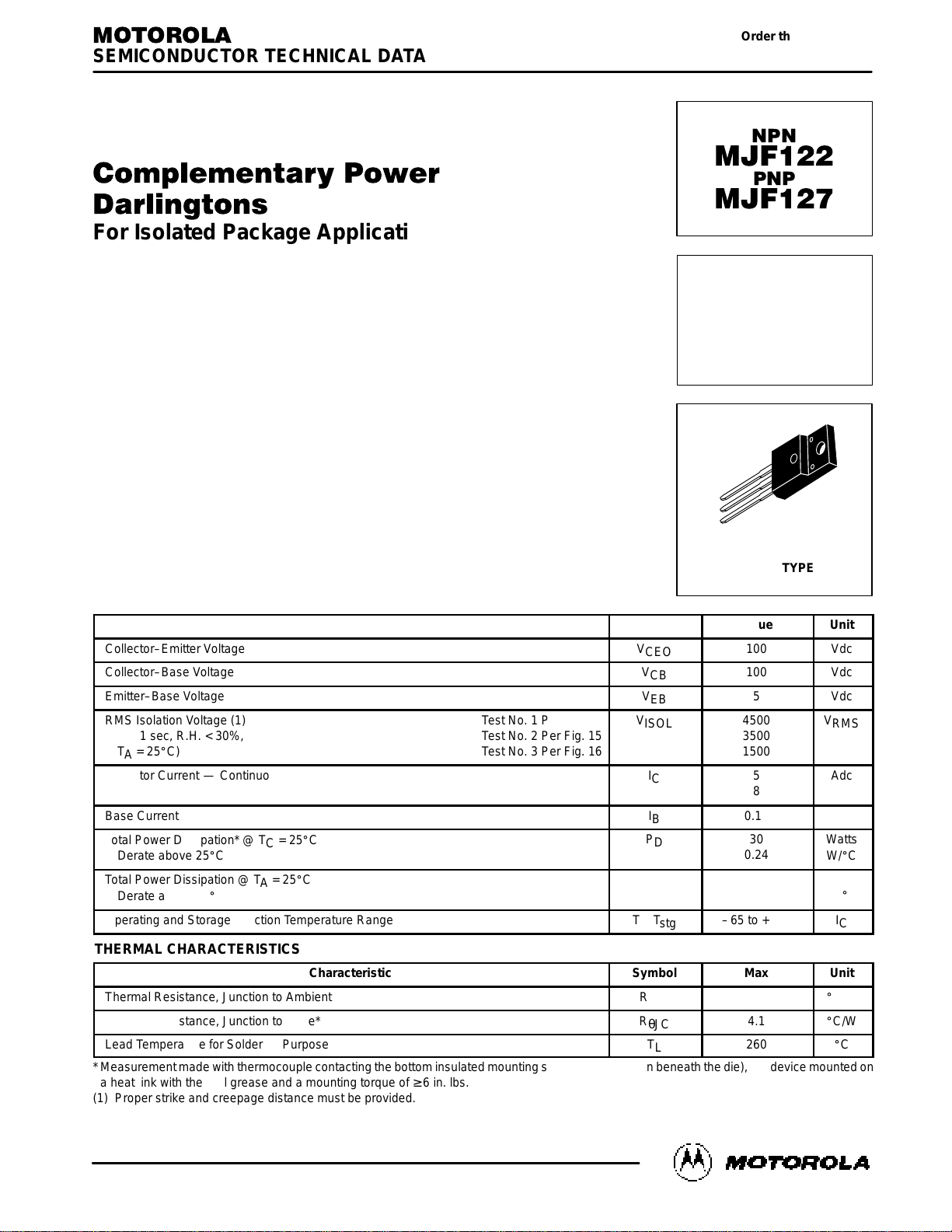
Page 1
1
Motorola Bipolar Power Transistor Device Data
For Isolated Package Applications
Designed for general–purpose amplifiers and switching applications, where the
mounting surface of the device is required to be electrically isolated from the heatsink
or chassis.
• Electrically Similar to the Popular TIP122 and TIP127
• 100 V
CEO(sus)
• 5 A Rated Collector Current
• No Isolating Washers Required
• Reduced System Cost
• High DC Current Gain — 2000 (Min) @ IC = 3 Adc
• UL Recognized, File #E69369, to 3500 V
RMS
Isolation
MAXIMUM RATINGS
Rating
Symbol
Value
ÎÎÎ
ÎÎÎ
ÎÎÎ
Unit
Collector–Emitter Voltage
V
CEO
100
ÎÎÎ
ÎÎÎ
ÎÎÎ
Vdc
Collector–Base Voltage
V
CB
100
ÎÎÎ
ÎÎÎ
ÎÎÎ
Vdc
Emitter–Base Voltage
V
EB
5
ÎÎÎ
ÎÎÎ
ÎÎÎ
Vdc
RMS Isolation Voltage (1) Test No. 1 Per Fig. 14
(for 1 sec, R.H. < 30%, Test No. 2 Per Fig. 15
TA = 25_C) Test No. 3 Per Fig. 16
V
ISOL
4500
3500
1500
ÎÎÎ
ÎÎÎ
ÎÎÎ
ÎÎÎ
ÎÎÎ
V
RMS
Collector Current — Continuous
Peak
I
C
5
8
ÎÎÎ
ÎÎÎ
ÎÎÎ
Adc
Base Current
I
B
0.12
ÎÎÎ
ÎÎÎ
ÎÎÎ
Adc
Total Power Dissipation* @ TC = 25_C
Derate above 25_C
P
D
30
0.24
ÎÎÎ
ÎÎÎ
ÎÎÎ
ÎÎÎ
Watts
W/_C
Total Power Dissipation @ TA = 25_C
Derate above 25_C
P
D
2
0.016
ÎÎÎ
ÎÎÎ
ÎÎÎ
ÎÎÎ
Watts
W/_C
Operating and Storage Junction Temperature Range
TJ, T
stg
–65 to +150
ÎÎÎ
ÎÎÎ
ÎÎÎ
I
C
THERMAL CHARACTERISTICS
Characteristic
Symbol
Max
ÎÎÎ
ÎÎÎ
ÎÎÎ
Unit
Thermal Resistance, Junction to Ambient
R
θJA
62.5
ÎÎÎ
ÎÎÎ
ÎÎÎ
_
C/W
Thermal Resistance, Junction to Case*
R
θJC
4.1
ÎÎÎ
ÎÎÎ
ÎÎÎ
_
C/W
Lead Temperature for Soldering Purpose
T
L
260
ÎÎÎ
ÎÎÎ
ÎÎÎ
_
C
*Measurement made with thermocouple contacting the bottom insulated mounting surface (in a location beneath the die), the device mounted on
a heatsink with thermal grease and a mounting torque of ≥ 6 in. lbs.
(1) Proper strike and creepage distance must be provided.
SEMICONDUCTOR TECHNICAL DATA
Order this document
by MF122/D
Motorola, Inc. 1995
COMPLEMENTARY
SILICON
POWER DARLINGTONS
5 AMPERES
100 VOLTS
30 WATTS
CASE 221D–02
TO–220 TYPE
Page 2
2
Motorola Bipolar Power Transistor Device Data
ELECTRICAL CHARACTERISTICS (T
C
= 25_C unless otherwise noted)
Characteristic
ÎÎÎÎ
ÎÎÎÎ
ÎÎÎÎ
Symbol
Min
Max
ÎÎÎ
ÎÎÎ
ÎÎÎ
Unit
OFF CHARACTERISTICS
Collector–Emitter Sustaining Voltage (1)
(IC = 100 mAdc, IB = 0)
ÎÎÎÎ
ÎÎÎÎ
ÎÎÎÎ
ÎÎÎÎ
V
CEO(sus)
100
—
ÎÎÎ
ÎÎÎ
ÎÎÎ
ÎÎÎ
Vdc
Collector Cutoff Current
(VCE = 50 Vdc, IB = 0)
ÎÎÎÎ
ÎÎÎÎ
ÎÎÎÎ
ÎÎÎÎ
I
CEO
—
10
ÎÎÎ
ÎÎÎ
ÎÎÎ
ÎÎÎ
µAdc
Collector Cutoff Current
(VCB = 100 Vdc, IE = 0)
ÎÎÎÎ
ÎÎÎÎ
ÎÎÎÎ
I
CBO
—
10
ÎÎÎ
ÎÎÎ
ÎÎÎ
µAdc
Emitter Cutoff Current (VBE = 5 Vdc, IC = 0)
ÎÎÎÎ
ÎÎÎÎ
ÎÎÎÎ
I
EBO
—
2
ÎÎÎ
ÎÎÎ
ÎÎÎ
mAdc
ON CHARACTERISTICS (1)
DC Current Gain (IC = 0.5 Adc, VCE = 3 Vdc)
DC Current Gain (IC = 3 Adc, VCE = 3 Vdc)
ÎÎÎÎ
ÎÎÎÎ
ÎÎÎÎ
ÎÎÎÎ
h
FE
1000
2000
—
—
ÎÎÎ
ÎÎÎ
ÎÎÎ
ÎÎÎ
—
Collector–Emitter Saturation Voltage (IC = 3 Adc, IB = 12 mAdc)
Collector–Emitter Saturation Voltage (IC = 5 Adc, IB = 20 mAdc)
ÎÎÎÎ
ÎÎÎÎ
ÎÎÎÎ
ÎÎÎÎ
V
CE(sat)
—
—
2
3.5
ÎÎÎ
ÎÎÎ
ÎÎÎ
ÎÎÎ
Vdc
Base–Emitter On Voltage (IC = 3 Adc, VCE = 3 Vdc)
ÎÎÎÎ
ÎÎÎÎ
ÎÎÎÎ
V
BE(on)
—
2.5
ÎÎÎ
ÎÎÎ
ÎÎÎ
Vdc
DYNAMIC CHARACTERISTICS
Small–Signal Current Gain (IC = 3 Adc, VCE = 4 Vdc, f = 1 MHz)
ÎÎÎÎ
ÎÎÎÎ
ÎÎÎÎ
h
fe
4
—
ÎÎÎ
ÎÎÎ
ÎÎÎ
—
Output Capacitance MJF127
(VCB = 10 Vdc, IE = 0, f = 0.1 MHz) MJF122
ÎÎÎÎ
ÎÎÎÎ
ÎÎÎÎ
ÎÎÎÎ
C
ob
—
—
300
200
ÎÎÎ
ÎÎÎ
ÎÎÎ
ÎÎÎ
pF
(1) Pulse Test: Pulse Width v 300 µs, Duty Cycle v 2%.
Figure 1. Switching Times Test Circuit
VCC = 30 V
IC/IB = 250
IB1 = I
B2
TJ = 25
°
C
0.1 0.7 100.5
0.3
2 5
5
IC, COLLECTOR CURRENT (AMP)
td @ V
BE(off)
= 0 V
t, TIME ( s)
µ
2
1
0.5
0.2
0.1
0.05
Figure 2. Typical Switching Times
t
s
t
f
0.3
3
0.2
1
0.07
0.7
3 7
PNP
NPN
≈
120
≈
8 k
V
2
APPROX.
+8 V
V
1
APPROX.
–12 V
25
µ
s
R
B
51
D
1
+4 V
V
CC
–30 V
R
C
SCOPE
TUT
tr, tf
≤
10 ns
DUTY CYCLE = 1%
FOR td AND tr, D1 IS DISCONNECTED
AND V2 = 0
FOR NPN TEST CIRCUIT REVERSE ALL POLARITIES.
RB & RC VARIED TO OBTAIN DESIRED CURRENT LEVELS
D1, MUST BE FAST RECOVERY TYPES, e.g.,
1N5825 USED ABOVE IB
≈
100 mA
MSD6100 USED BELOW IB
≈
100 mA
t
r
0
Page 3

3
Motorola Bipolar Power Transistor Device Data
P
D
, POWER DISSIPATION (WATTS)
0
80
60
40
20
4
3
2
1
TAT
C
0
Figure 3. Maximum Power Derating
T, TEMPERATURE (°C)
40 60 100 120 16080 140
T
C
20
t, TIME (ms)
0.01
0.1 0.5 10 20 50 100 200 500 5K 10K1 52
1
0.2
0.1
0.05
r(t), TRANSIENT THERMAL
SINGLE PULSE
R
θ
JC(t)
= r(t) R
θ
JC
T
J(pk)
– TC = P
(pk)
R
θ
JC
(t)
RESISTANCE (NORMALIZED)
Figure 4. Thermal Response
0.5
0.3
0.03
0.02
0.2
1K 2K30 3003
0.3
3K
T
A
VCE, COLLECTOR–EMITTER VOLTAGE (VOLTS)
Figure 5. Maximum Forward Bias
Safe Operating Area
1
10
1
30
CURRENT LIMIT
SECONDARY BREAKDOWN
LIMIT
THERMAL LIMIT @
TC = 25
°
C (SINGLE PULSE)
I
C
, COLLECTOR CURRENT (AMPS)
0.1
2 3 50
3
0.3
10
0.2
dc
TJ = 150°C
1 ms
5 ms
100 µs
2
5
0.5
5 10020
There are two limitations on the power handling ability of a
transistor: average junction temperature and second breakdown. Safe operating area curves indicate IC – VCE limits of
the transistor that must be observed for reliable operation;
i.e., the transistor must not be subjected to greater dissipation than the curves indicate.
The data of Figure 5 is based on T
J(pk)
= 150_C; TC is
variable depending on conditions. Secondary breakdown
pulse limits are valid for duty cycles to 10% provided T
J(pk)
< 150_C. T
J(pk)
may be calculated from the data in Figure 4.
At high case temperatures, thermal limitations will reduce the
power that can be handled to values less than the limitations
imposed by secondary breakdown.
Page 4

4
Motorola Bipolar Power Transistor Device Data
V
CE
, COLLECTOR–EMITTER VOLTAGE (VOLTS)
V
CE
, COLLECTOR–EMITTER VOLTAGE (VOLTS)
Figure 6. Typical Small–Signal Current Gain
f, FREQUENCY (kHz)
70
300
h
fe
, SMALL–SIGNAL CURRENT GAIN
30
200
100
50
TC = 25°C
VCE = 4 Vdc
IC = 3 Adc
Figure 7. Typical Capacitance
10,000
VR, REVERSE VOLTAGE (VOLTS)
C, CAPACITANCE (pF)
C
ib
C
ob
0.1
200
100
1000
500
300
10
30
100510.5
2000
3000
5000
10 500.2 2 20
TJ = 25°C
IC, COLLECTOR CURRENT (AMP)
NPN
MJF122
PNP
MJF127
Figure 8. Typical DC Current Gain
0.1
IC, COLLECTOR CURRENT (AMP)
200
0.2 0.5
3000
1000
10,000
h
FE
, DC CURRENT GAIN
VCE = 4 V
TJ = 150°C
5000
0.3 1
25°C
–55°C
2000
0.7 3
20,000
300
500
5 10
h
FE
, DC CURRENT GAIN
IB, BASE CURRENT (mA)
2.6
2.2
1.8
1.4
0.3 0.5 0.7 102 5
IC = 2 A
4 A
1
6 A
TJ = 25°C
3
1
20 30
IB, BASE CURRENT (mA)
2.6
2.2
1.8
1.4
3
1
Figure 9. Typical Collector Saturation Region
PNP
NPN
PNP
NPN
1 100050105 100 5002 20 200
20
50
200
3000
1000
10,000
5000
2000
20,000
300
500
2 7 0.1 0.2 0.50.3 10.7 3 5 102 7
VCE = 4 V
TJ = 150°C
25°C
–55°C
IC = 2 A
4 A
6 A
700
7000
3 7 0.3 0.5 0.7 102 51 20 303 7
TJ = 25°C
Page 5

5
Motorola Bipolar Power Transistor Device Data
V
, TEMPERATURE COEFFICIENTS (mV/ C)
°θ
0.1
NPN
MJF122
PNP
MJF127
10
–1
0+0.4 –0.2 –0.4 –0.6+0.6 +0.2 –0.8 –1 –1.2 –1.4
IC, COLLECTOR CURRENT (AMP)
0
*IC/IB ≤ hFE
3
– 5
10
4
VBE, BASE–EMITTER VOLTAGE (VOLTS)
10
–1
0– 0.4
, COLLECTOR CURRENT ( A)
µ
I
C
10
3
10
2
10
1
10
0
+0.2 +0.4 +0.6
TJ = 150°C
100°C
REVERSE
FORWARD
25°C
VCE = 30 V
10
5
–0.6 – 0.2 +0.8 +1 +1.2 +1.4
10
4
VBE, BASE–EMITTER VOLTAGE (VOLTS)
, COLLECTOR CURRENT ( A)
µ
I
C
10
3
10
2
10
1
10
0
TJ = 150°C
100°C
REVERSE FORWARD
25°C
VCE = 30 V
10
5
– 4
– 3
– 2
– 1
θ
VB
FOR V
BE
25°C to 150°C
*
θ
VC
FOR V
CE(sat)
IC, COLLECTOR CURRENT (AMP)
Figure 10. Typical “On” Voltages
Figure 11. Typical Temperature Coefficients
0.1
IC, COLLECTOR CURRENT (AMP)
2
1.5
V, VOLTAGE (VOLTS)
3
2.5
1
0.5
0.2 0.5 50.3 10.7 3 10
IC, COLLECTOR CURRENT (AMP)
2
1.5
V, VOLTAGE (VOLTS)
3
2.5
1
0.5
TJ = 25°C
V
BE(sat)
@ IC/IB = 250
VBE @ VCE = 4 V
TJ = 25°C
V
BE(sat)
@ IC/IB = 250
VBE @ VCE = 4 V
V
CE(sat)
@ IC/IB = 250
V
, TEMPERATURE COEFFICIENT (mV C)
°θ
72 0.1 0.2 0.5 50.3 10.7 3 1072
0.2 0.5 50.3 10.7 3 1072 0.1 0.2 0.5 50.3 1 3 1072
+ 1
+ 2
+ 3
+ 4
+ 5
0
– 5
– 4
– 3
– 2
– 1
+ 1
+ 2
+ 3
+ 4
+ 5
– 55°C to 25°C
*IC/IB ≤ hFE
3
θ
VB
FOR V
BE
*
θ
VC
FOR V
CE(sat)
Figure 12. Typical Collector Cut–Off Region
V
CE(sat)
@ IC/IB = 250
25°C to 150°C
– 55°C to 25°C
25°C to 150°C
– 55°C to 25°C
25°C to 150°C
– 55°C to 25°C
Page 6

6
Motorola Bipolar Power Transistor Device Data
BASE
EMITTER
COLLECTOR
≈
8 k≈ 120
BASE
EMITTER
COLLECTOR
≈
8 k≈ 120
NPN
MJF122
PNP
MJF127
Figure 13. Darlington Schematic
MOUNTED
FULLY ISOLATED
PACKAGE
LEADS
HEATSINK
0.110” MIN
Figure 14. Clip Mounting Position
for Isolation Test Number 1
*Measurement made between leads and heatsink with all leads shorted together
CLIP
CLIP
0.107” MIN
LEADS
HEATSINK
0.107” MIN
Figure 15. Clip Mounting Position
for Isolation Test Number 2
Figure 16. Screw Mounting Position
for Isolation Test Number 3
MOUNTED
FULLY ISOLATED
PACKAGE
MOUNTED
FULLY ISOLATED
PACKAGE
LEADS
HEATSINK
TEST CONDITIONS FOR ISOLATION TESTS*
4–40 SCREW
PLAIN WASHER
HEATSINK
COMPRESSION WASHER
NUT
CLIP
HEATSINK
Laboratory tests on a limited number of samples indicate, when using the screw and compression washer mounting technique, a screw
torque of 6 to 8 in.lbs is sufficient to provide maximum power dissipation capability . The compression washer helps to maintain a constant pressure on the package over time and during large temperature excursions.
Destructive laboratory tests show that using a hex head 4–40 screw, without washers, and applying a torque in excess of 20 in.lbs will
cause the plastic to crack around the mounting hole, resulting in a loss of isolation capability.
Additional tests on slotted 4–40 screws indicate that the screw slot fails between 15 to 20 in.lbs without adversely affecting the package. However, in order to positively ensure the package integrity of the fully isolated device, Motorola does not recommend exceeding 10
in.lbs of mounting torque under any mounting conditions.
Figure 17. Typical Mounting Techniques*
MOUNTING INFORMATION
**For more information about mounting power semiconductors see Application Note AN1040.
Page 7

7
Motorola Bipolar Power Transistor Device Data
PACKAGE DIMENSIONS
CASE 221D–02
TO–220 TYPE
ISSUE D
NOTES:
1. DIMENSIONING AND TOLERANCING PER ANSI
Y14.5M, 1982.
2. CONTROLLING DIMENSION: INCH.
STYLE 2:
PIN 1. BASE
2. COLLECTOR
3. EMITTER
DIMAMIN MAX MIN MAX
MILLIMETERS
0.621 0.629 15.78 15.97
INCHES
B 0.394 0.402 10.01 10.21
C 0.181 0.189 4.60 4.80
D 0.026 0.034 0.67 0.86
F 0.121 0.129 3.08 3.27
G 0.100 BSC 2.54 BSC
H 0.123 0.129 3.13 3.27
J 0.018 0.025 0.46 0.64
K 0.500 0.562 12.70 14.27
L 0.045 0.060 1.14 1.52
N 0.200 BSC 5.08 BSC
Q 0.126 0.134 3.21 3.40
R 0.107 0.111 2.72 2.81
S 0.096 0.104 2.44 2.64
U 0.259 0.267 6.58 6.78
–B–
–Y–
G
N
D
L
K
H
A
F
Q
3 PL
1 2 3
M
B
M
0.25 (0.010) Y
SEATING
PLANE
–T–
U
C
S
J
R
Page 8
8
Motorola Bipolar Power Transistor Device Data
How to reach us:
USA /EUROPE: Motorola Literature Distribution; JAPAN: Nippon Motorola Ltd.; Tatsumi–SPD–JLDC, Toshikatsu Otsuki,
P.O. Box 20912; Phoenix, Arizona 85036. 1–800–441–2447 6F Seibu–Butsuryu–Center, 3–14–2 Tatsumi Koto–Ku, Tokyo 135, Japan. 03–3521–8315
MFAX: RMFAX0@email.sps.mot.com – TOUCHTONE (602) 244–6609 HONG KONG: Motorola Semiconductors H.K. Ltd.; 8B Tai Ping Industrial Park,
INTERNET: http://Design–NET.com 51 Ting Kok Road, Tai Po, N.T., Hong Kong. 852–26629298
Motorola reserves the right to make changes without further notice to any products herein. Motorola makes no warranty , representation or guarantee regarding
the suitability of its products for any particular purpose, nor does Motorola assume any liability arising out of the application or use of any product or circuit,
and specifically disclaims any and all liability, including without limitation consequential or incidental damages. “T ypical” parameters can and do vary in different
applications. All operating parameters, including “T ypicals” must be validated for each customer application by customer’s technical experts. Motorola does
not convey any license under its patent rights nor the rights of others. Motorola products are not designed, intended, or authorized for use as components in
systems intended for surgical implant into the body, or other applications intended to support or sustain life, or for any other application in which the failure of
the Motorola product could create a situation where personal injury or death may occur. Should Buyer purchase or use Motorola products for any such
unintended or unauthorized application, Buyer shall indemnify and hold Motorola and its officers, employees, subsidiaries, affiliates, and distributors harmless
against all claims, costs, damages, and expenses, and reasonable attorney fees arising out of, directly or indirectly, any claim of personal injury or death
associated with such unintended or unauthorized use, even if such claim alleges that Motorola was negligent regarding the design or manufacture of the part.
Motorola and are registered trademarks of Motorola, Inc. Motorola, Inc. is an Equal Opportunity/Affirmative Action Employer.
MJF122/D
*MJF122/D*
◊
 Loading...