

Page 1
MJE2955T
MJE3055T
COMPLEMENTARY SILICON POWER TRANSISTORS
■ SGS-THOMS O N PREF ERRE D SA LES TYP E S
■ COMPLEMEN TA RY PNP - NPN DEVI CES
DESCRIPTION
The MJE3055T is a silicon epitaxial-base NPN
transistor in Jedec TO-220 package. It is
intended for power switching circuits and
general-purpose amplifiers. The complementary
PNP type is MJE2955T.
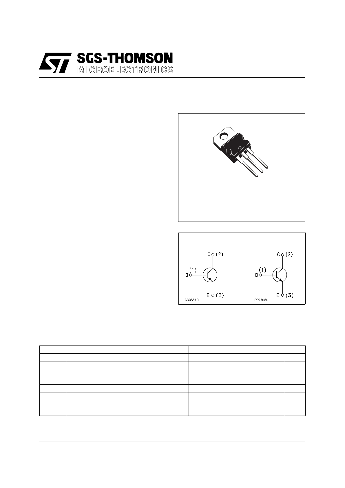
TO-220
3
2
1
INTERNAL SCHEMATIC DIAGRAM
ABSOL UT E MAXIMU M RATINGS
Symbol Parameter Value Unit
V
V
V
P
T
For PNP types voltage and current values are negative.
Collector-Emitter Voltage (IB = 0) 60 V
CEO
Collector-Base Voltage (IE = 0) 70 V
CBO
Emitter-Base Voltage (IC = 0) 5 V
EBO
Collector Current 10 A
I
C
Base Current 6 A
I
B
Total Power Dissipation at T
tot
Storage Temperature -55 to 150
stg
Max. Operating Junction Temperature 150
T
j
≤ 25 oC75W
case
o
C
o
C
June 1997
1/4
Page 2

MJE2955T / MJE3055T
THERMAL DATA
R
thj-case
Thermal Resistance Junction-case Max 1.66
o
C/W
ELECTRICAL CHARACTERISTICS (T
= 25 oC unless otherwise specified)
case
Symbol Parameter Test Conditions Min. Typ. Max. Unit
I
CEO
I
CEX
I
CBO
I
EBO
V
CEO(sus)
Collector Cut-off
Current (I
= 0)
B
Collector Cut-off
Current (V
= 1.5V)
BE
Collector Cut-off
Current (I
= 0)
E
Emitter Cut-off Current
(I
= 0)
C
∗ Collector-Emitter
= 30 V 700 µA
V
CE
= 70 V
V
CE
T
V
T
V
150oC
CASE =
= 70 V
CBO
150oC
CASE =
= 5 V 5 mA
EBO
1
5
1
10
IC = 200 mA 60 V
Sustaining Voltage
V
∗ Collector-Emitter
CE(sat)
Sustaining Voltage
V
∗ Base-Emitter on
BE(on)
IC = 4 A IB = 0.4 A
I
= 10 A IB = 3.3 A
C
1.1
8
IC = 4 A VCE = 4 V 1.8 V
Voltage
h
f
DC Current Gain IC = 4 A VCE = 4 V
FE
Transistor Frequency IC = 500 mA VCE = 10 V
T
I
= 10 A VCE = 4 V
C
20
70
5
2 MHz
f = 500 KHz
∗ Pulsed: Pulse duration = 300µs, duty cycle ≤ 2 %
For PNP type voltage and current values are negative.
mA
mA
mA
mA
V
V
2/4
Page 3

E
TO-220 MECHANICAL DATA
MJE2955T / MJE3055T
DIM.
A 4.40 4.60 0.173 0.181
C 1.23 1.32 0.048 0.051
D 2.40 2.72 0.094 0.107
D1 1.27 0.050
E 0.49 0.70 0.019 0.027
F 0.61 0.88 0.024 0.034
F1 1.14 1.70 0.044 0.067
F2 1.14 1.70 0.044 0.067
G 4.95 5.15 0.194 0.203
G1 2.4 2.7 0.094 0.106
H2 10.0 10.40 0.393 0.409
L2 16.4 0.645
L4 13.0 14.0 0.511 0.551
L5 2.65 2.95 0.104 0.116
L6 15.25 15.75 0.600 0.620
L7 6.2 6.6 0.244 0.260
L9 3.5 3.93 0.137 0.154
DIA. 3.75 3.85 0.147 0.151
MIN. TYP. MAX. MIN. TYP. MAX.
mm inch
A
C
D
L5
Dia.
L7
D1
L6
L2
L9
F1
G1
H2
G
F
F2
L4
P011C
3/4
Page 4

MJE2955T / MJE3055T
4/4
Information furnished is believed to be accurate and reliable. However, SGS-THOMSON Microelectronics assumes no responsability for the
consequences of use of such information nor for any infringement of patents or other rights of third parties which may results from its use. No
license is granted by implication or ot he rwise under any patent or patent rights of SGS-THOMSON Microelectronics. Specificati ons mentioned
in this publication are subject to change without notice. This publication supersedes and replaces all information previously supplied.
SGS-THOMSON Microelectronics products are not authorized for use as critical components in life support devices o r systems without express
written approval of SGS-THOMSON Microelectonics.
© 1997 SGS-THOMSON Microelectronics - Printed in Italy - All Rights Reserved
Australia - Brazil - Canada - China - France - Germany - Hong Kong - Italy - Japan - Korea - Malaysia - Malta - Morocco - The Netherlands -
Singapore - Spain - Sweden - Switzerland - Taiwan - Thailand - United Kingdom - U.S.A
SGS-THOMSON Microelectronics GROUP OF COMPANIES
. . .
 Loading...