

Page 1
■ SGS-THOMS O N PREF ERRE D SA LES TYP E
■ PNP TRANS IS T OR
DESCRIPTION
The MJE210 is a silicon epitaxial-base PNP
transistor in Jedec SOT-32 plastic package,
designed for low voltage, low power, high gain
aydio amplifier applications.
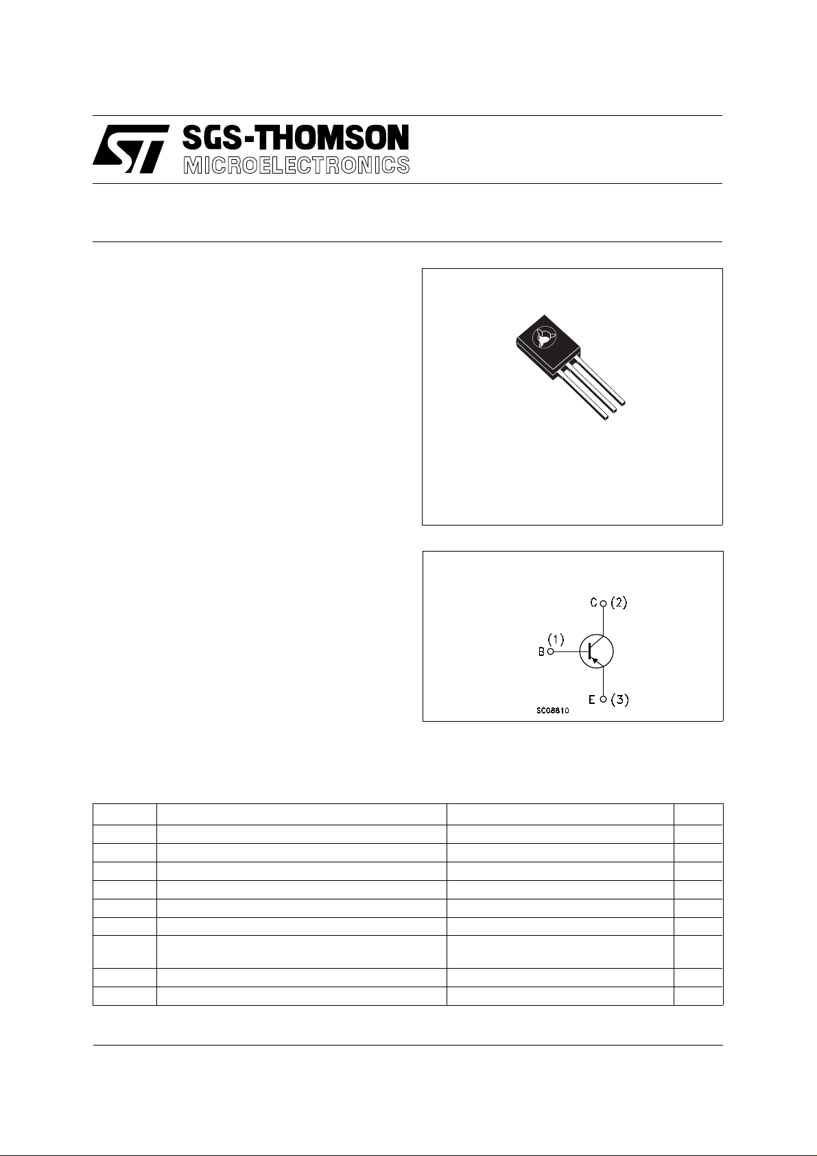
MJE210
SILI CON PNP TRANSISTOR
1
2
3
SOT-32
INTERNAL SCHEMATIC DIAGRAM
ABSOLUT E MAXIMUM RATI NG S
Symbol Parameter Value Unit
V
V
V
I
P
T
Collector-Base Voltage (IE = 0) -40 V
CBO
Collector-Emitter Voltage (IB = 0) -25 V
CEO
Base-Emitter Voltage (IC = 0) -8 V
EBO
Collector Current -5 A
I
C
Collector Peak Current -10 A
CM
Base Current -1 A
I
B
Total Power Dissipation at T
tot
at T
Storage Temperature -65 to 150
stg
Max Operating Junction Temperature 150
T
j
case
amb
≤ 25 oC
≤ 25 oC
15
1.5
W
o
C
o
C
September 1997
1/4
Page 2

MJE210
THERMAL DATA
R
thj-amb
R
thj-case
Thermal Resistance Junction-ambient Max
Thermal Resistance Junction-case Max
83.4
8.34
o
C/W
o
C/W
ELECTRICAL CHARACTERISTICS (T
= 25 oC unless otherwise specified)
case
Symbol Parameter Test Conditions Min. Typ. Max. Unit
I
CBO
I
EBO
V
CEO(sus)
Collector Cut-off
Current (I
= 0)
E
Emitter Cut-off Current
(I
= 0)
C
Collector-Emitter
∗
Sustaining Voltage
Collector-Emitter
∗
V
CE(sat)
V
BE(sat)
V
BE
Sustaining Voltage
Base-Emitter on
∗
Voltage
Base-Emitter on
∗
Voltage
DC Current Gain I
∗
h
FE
f
C
CBO
∗ Pulsed: Pulse duration = 300µs, duty cycle ≤ 1.5%
Transistor Frequency IC = 0.1 A VCE = 10 V
T
Collector-base
Capacitance
= -40 V
V
CB
V
= -40 V T
CB
= -8 V
V
EB
I
= -10 mA
C
= -0.5 A IB = -50 mA
I
C
I
= -2 A IB = -0.2 A
C
I
= -5 A IB = -1 A
C
= -5 A IB = -1 A
I
C
=- 2 A VCE = -1 V -1.6 V
I
C
= -0.5 A VCE = -1 V
C
I
= -2 A VCE = -1 V
C
I
= -5 A VCE = -2 V
C
f = 10 MHz
CASE =
125oC
-25 V
70
45
10
65 MHz
-100
-100nAµA
-100 nA
-0.3
-0.75
-1.8
-2.5
180
VCB = -10 V IE = 0 f = 0.1 MHz 120 pF
V
V
V
V
2/4
Page 3

SOT-32 (TO-126) MECHANICAL DATA
MJE210
DIM.
MIN. TYP. MAX. MIN. TYP. MAX.
A 7.4 7.8 0.291 0.307
B 10.5 10.8 0.413 0.445
b 0.7 0.9 0.028 0.035
b1 0.49 0.75 0.019 0.030
C 2.4 2.7 0.040 0.106
c1 1.0 1.3 0.039 0.050
D 15.4 16.0 0.606 0.629
e2.2 0.087
e3 4.15 4.65 0.163 0.183
F3.8 0.150
G 3 3.2 0.118 0.126
H2.540.100
H2 2.15 0.084
mm inch
H2
0016114
3/4
Page 4

MJE210
4/4
Information furnished is believed to be accurate and reliable. However, SGS-THOMSON Microelectronics assumes no responsability for the
consequences of use of such information nor for any infringement of patents or other rights of third parties which may results from its use. No
license is granted by implication or ot he rwise under any patent or patent rights of SGS-THOMSON Microelectronics. Specificati ons mentioned
in this publication are subject to change without notice. This publication supersedes and replaces all information previously supplied.
SGS-THOMSON Microelectronics products are not authorized for use as critical components in life support devices or systems wi thout express
written approval of SGS-THOMSON Microelectonics.
© 1997 SGS-THOMSON Microelectronics - Printed in Italy - All Rights Reserved
Australia - Brazil - Canada - China - France - Germany - Hong Kong - Italy - Japan - Korea - Malaysia - Malta - Morocco - The Netherlands -
Singapore - Spain - Sweden - Switzerland - Taiwan - Thailand - United Kingdom - U.S.A
SGS-THOMSON Microelectronics GROUP OF COMPANIES
. . .
 Loading...