

Page 1
MJE172
®
MJE182
COMPLEMENTARY SILICON POWER TRANSISTORS
■ SGS-THOMS O N PREF ERRE D SA LES TYP E S
■ COMPLEMEN TA RY PNP - NPN DEVI CES
DESCRIPTION
The MJE172 (PNP type) and MJE182 (NPN type)
are silicon epitaxial planar, complementary
transistors in Jedec SOT-32 plastic package, they
are designed for low power audio amplifier and
low current, high speed switching applications.
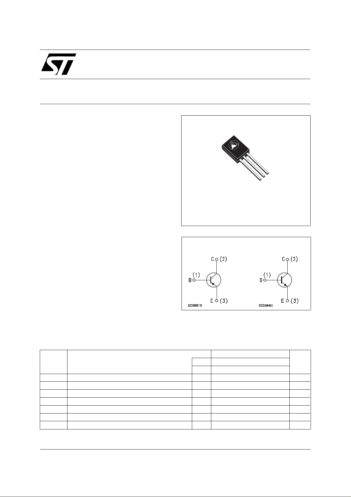
SOT-32
1
2
3
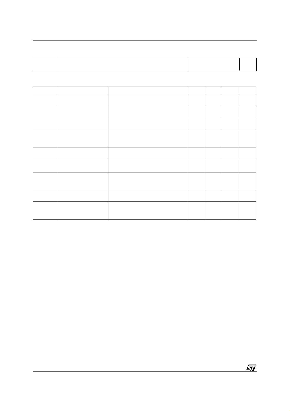
INTERNAL SCHEMATIC DIAGRAM
ABSOLUT E MAXIMUM RATI NG S
Symbol Parameter Value Unit
NPN MJE182
PNP MJE172
V
V
V
I
P
Collector-Emitter Voltage (IB = 0) 80 80 V
CEO
Collector-Base Voltage (IE = 0) 100 100 V
CBO
Base-Emitter Voltage (IC = 0) 7 7 V
EBO
Collector Current 3 3 A
I
C
Collector Peak Current 6 6 A
CM
Base Current 1 1 A
I
B
Total Power Dissipation at T
tot
≤ 25 oC 12.5 12.5 W
case
September 1998
1/4
Page 2
MJE172 - MJE182
THERMAL DATA
R
thj-amb
R
thj-case
Thermal Resistance Junction-ambient Max
Thermal Resistance Junction-case Max
83.4
10
o
C/W
o
C/W
ELECTRICAL CHARACTERISTICS (T
= 25 oC unless otherwise specified)
case
Symbol Parameter Test Conditions Min. Typ. Max. Unit
I
CBO
I
EBO
V
CEO(sus)
Collector Cut-off
Current (I
= 0)
E
Emitter Cut-off Current
(I
= 0)
C
∗ Collector-Emitter
= rated V
V
CB
T
CASE =
= 7 V 0.1 µA
V
EB
CBO
150oC
0.1
0.1
IC = 10 mA 80 V
Sustaining Voltage
V
∗ Collector-Emitter
CE(sat)
Saturation Voltage
V
∗ Base-Emitter on
BE(sat)
Voltage
VBE∗ Base-Emitter on
IC = 0.5 A IB = 50 mA
I
= 1.5 A IB = 0.15 A
C
I
= 3 A IB = 0.6 A
C
IC = 1.5 A IB = 0.15 A
I
= 3 A IB = 0.6 A
C
IC = 0.5 A VCE = 1 V 1.2 V
0.3
0.9
1.7
1.5
2
Voltage
h
f
DC Current Gain IC = 0.1 A VCE = 1 V
FE
Transistor Frequency IC = 0.1 A VCE = 10 V
T
I
= 0.5 A VCE = 1 V
C
I
= 1.5 A VCE = 1 V
C
50
250
30
12
50 MHz
f = 10 MHz
C
CBO
Collector-base
Capacitance
∗ Pulsed: Pulse duration = 300µs, duty cycle ≤ 1.5%
For PNP type voltage and current values are negative.
VCB = 10 V IE = 0 f = 0.1MHz
for MJE172
for MJE182
60
40
µA
mA
V
V
V
V
pF
pF
2/4
Page 3

SOT-32 (TO-126) MECHANICAL DATA
MJE172 - MJE182
DIM.
MIN. TYP. MAX. MIN. TYP. MAX.
A 7.4 7.8 0.291 0.307
B 10.5 10.8 0.413 0.445
b 0.7 0.9 0.028 0.035
b1 0.49 0.75 0.019 0.030
C 2.4 2.7 0.040 0.106
c1 1.0 1.3 0.039 0.050
D 15.4 16.0 0.606 0.629
e 2.2 0.087
e3 4.15 4.65 0.163 0.183
F 3.8 0.150
G 3 3.2 0.118 0.126
H 2.54 0.100
H2 2.15 0.084
mm inch
H2
c1
0016114
3/4
Page 4

MJE172 - MJE182
Information furnished is believed to be accurate and reliable. However, STMicroelectronics assumes no responsibility for the consequences
of use of such information nor for any infringement of patents or other rights of third parties which m ay result fro m its use. No license is
granted by implication or otherwise und er any patent or patent rights of STMicroelectronics. Specification mentioned in this publication are
subject to change without notice. This publication supersedes and replaces all information previously supplied. STMicroelectronics products
are not authorized for use as critical components in life support devices or systems witho ut express written approval of STMicroelectronics.
Australia - Brazil - Canada - China - France - Germany - Italy - Japan - Korea - Malaysia - Malta - Mexico - Morocco - The Netherl an ds -
Singapore - Spain - Sweden - Switzerland - Taiwan - Thailand - United Kingdom - U.S.A.
The ST logo is a registered trademark of STMicroelectronics
© 1998 STMicroelectronics – Printed in Italy – All Rights Reserved
STMicroelect r o nics G ROU P OF COM PANI E S
.
4/4
 Loading...