

Page 1
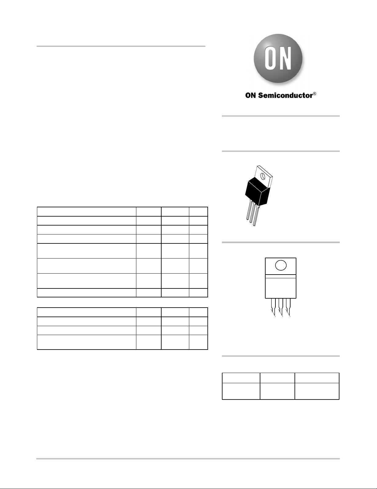
MJE18006G
SWITCHMODEt
NPN Bipolar Power Transistor
For Switching Power Supply Applications
The MJE18006G has an applications specific state−of−the−art die
designed for use in 220 V line−operated SWITCHMODE Power
supplies and electronic light ballasts.
Features
• Improved Efficiency Due to Low Base Drive Requirements:
♦ High and Flat DC Current Gain h
♦ Fast Switching
♦ No Coil Required in Base Circuit for Turn−Off (No Current Tail)
FE
• Tight Parametric Distributions are Consistent Lot−to−Lot
• Standard TO−220
• These Devices are Pb−Free and are RoHS Compliant*
MAXIMUM RATINGS
Rating Symbol Value Unit
Collector−Emitter Sustaining Voltage V
Collector−Emitter Breakdown Voltage V
Emitter−Base Voltage V
Collector Current − Continuous
− Peak (Note 1)
Base Current − Continuous
− Peak (Note 1)
Total Device Dissipation @ TC = 25_C
Derate above 25°C
Operating and Storage Temperature TJ, T
CEO
CES
EBO
I
I
CM
I
I
BM
P
C
B
D
stg
THERMAL CHARACTERISTICS
Characteristics Symbol Max Unit
Thermal Resistance, Junction−to−Case
Thermal Resistance, Junction−to−Ambient
Maximum Lead Temperature for Soldering
Purposes 1/8″ from Case for 5 Seconds
Stresses exceeding Maximum Ratings may damage the device. Maximum
Ratings are stress ratings only. Functional operation above the Recommended
Operating Conditions is not implied. Extended exposure to stresses above the
Recommended Operating Conditions may affect device reliability.
1. Pulse Test: Pulse Width = 5 ms, Duty Cycle ≤ 10%.
R
q
JC
R
q
JA
T
L
450 Vdc
1000 Vdc
9.0 Vdc
6.0
15
4.0
8.0
100
0.8
−65 to 150
1.25
62.5
260
Adc
Adc
W
W/_C
_C
_C/W
_C/W
_C
http://onsemi.com
POWER TRANSISTOR
6.0 AMPERES
1000 VOLTS − 100 WATTS
TO−220AB
CASE 221A−09
STYLE 1
1
2
3
MARKING DIAGRAM
MJE18006G
AY WW
A = Assembly Location
Y = Year
WW = Work Week
G = Pb−Free Package
ORDERING INFORMATION
Device Package Shipping
*For additional information on our Pb−Free strategy and soldering details, please
download the ON Semiconductor Soldering and Mounting Techniques
Reference Manual, SOLDERRM/D.
© Semiconductor Components Industries, LLC, 2010
April, 2010 − Rev. 7
1 Publication Order Number:
MJE18006G TO−220
(Pb−Free)
50 Units / Rail
MJE18006/D
Page 2
MJE18006G
ООООО
ООООО
ООООО
ООООО
ООООО
ООООО
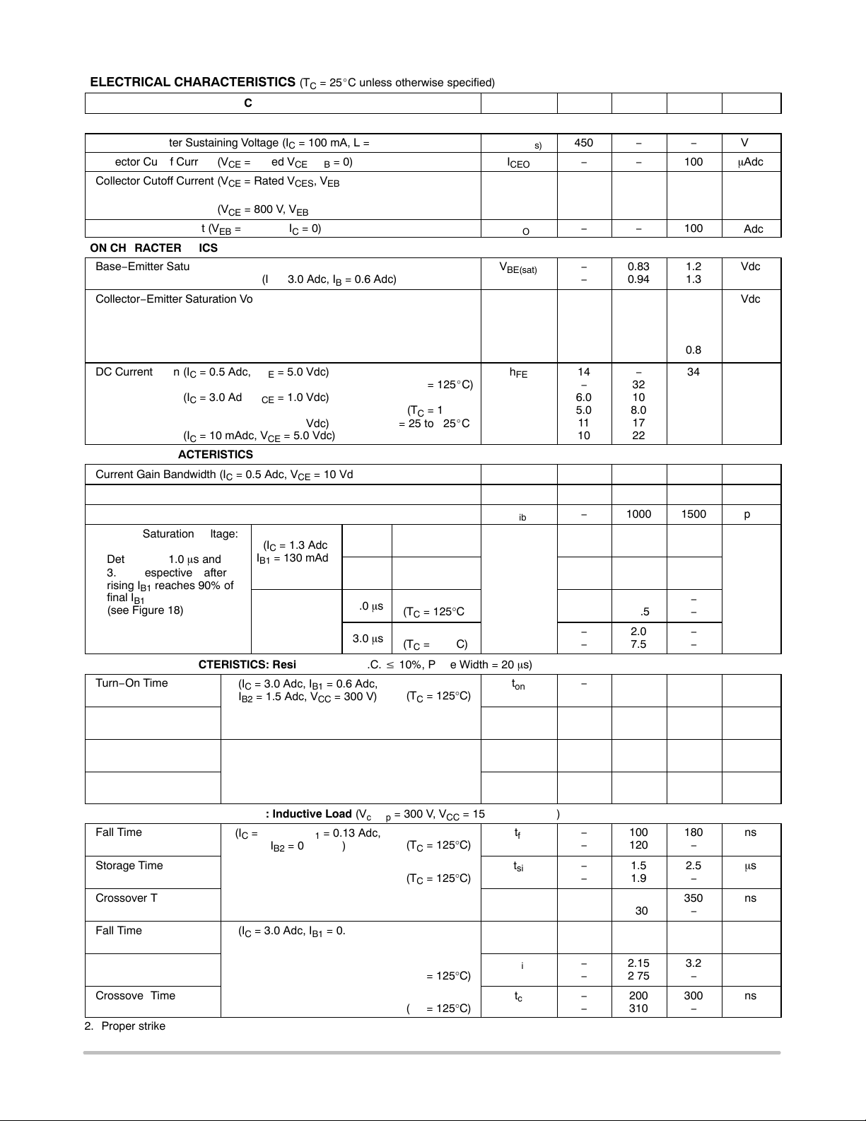
ELECTRICAL CHARACTERISTICS (T
Characteristic
= 25_C unless otherwise specified)
C
Symbol
OFF CHARACTERISTICS
Collector−Emitter Sustaining Voltage (IC = 100 mA, L = 25 mH)
Collector Cutoff Current (VCE = Rated V
Collector Cutoff Current (VCE = Rated V
CEO
, VEB = 0)
CES
, IB = 0)
(T
= 125_C)
C
V
CEO(sus)
I
CEO
I
CES
Collector Cutoff Current (VCE = 800 V, VEB = 0) (TC = 125_C)
Emitter Cutoff Current (VEB = 9.0 Vdc, IC = 0)
I
EBO
ON CHARACTERISTICS
Base−Emitter Saturation Voltage (IC = 1.3 Adc, IB = 0.13 Adc)
Base−Emitter Saturation Voltage (IC = 3.0 Adc, IB = 0.6 Adc)
Collector−Emitter Saturation Voltage
(IC = 1.3 Adc, IB = 0.13 Adc)
V
BE(sat)
V
CE(sat)
(TC = 125_C)
(IC = 3.0 Adc, IB = 0.6 Adc)
(TC = 125_C)
DC Current Gain (IC = 0.5 Adc, VCE = 5.0 Vdc)
h
(TC = 125_C)
DC Current Gain (IC = 3.0 Adc, VCE = 1.0 Vdc)
(TC = 125_C)
DC Current Gain (IC = 1.3 Adc, VCE = 1.0 Vdc) (TC = 25 to 125_C)
DC Current Gain (IC = 10 mAdc, VCE = 5.0 Vdc)
DYNAMIC CHARACTERISTICS
Current Gain Bandwidth (IC = 0.5 Adc, VCE = 10 Vdc, f = 1.0 MHz)
Output Capacitance (VCB = 10 Vdc, IE = 0, f = 1.0 MHz)
Input Capacitance (VEB = 8.0 V)
Dynamic Saturation Voltage:
Determined 1.0 ms and
3.0 ms respectively after
(IC = 1.3 Adc
IB1 = 130 mAdc
VCC = 300 V)
1.0 ms
3.0 ms
rising IB1 reaches 90% of
final I
B1
(see Figure 18)
(IC = 3.0 Adc
1.0 ms
IB1 = 0.6 Adc
VCC = 300 V)
3.0 ms
(TC = 125°C)
(TC = 125°C)
(TC = 125°C)
(TC = 125°C)
C
C
V
CE(dsat)
SWITCHING CHARACTERISTICS: Resistive Load (D.C. v 10%, Pulse Width = 20 ms)
Turn−On Time
(IC = 3.0 Adc, IB1 = 0.6 Adc,
IB2 = 1.5 Adc, VCC = 300 V)
(TC = 125°C)
Turn−Off Time
(TC = 125°C)
Turn−On Time
(IC = 1.3 Adc, IB1 = 0.13 Adc,
IB2 = 0.65 Adc, VCC = 300 V)
(TC = 125°C)
Turn−Off Time
(TC = 125°C)
SWITCHING CHARACTERISTICS: Inductive Load (V
Fall Time
(IC = 1.5 Adc, IB1 = 0.13 Adc,
IB2 = 0.65 Adc)
= 300 V, VCC = 15 V, L = 200 mH)
clamp
(TC = 125°C)
Storage Time
(TC = 125°C)
Crossover Time
(TC = 125°C)
Fall Time
(IC = 3.0 Adc, IB1 = 0.6 Adc,
IB2 = 1.5 Adc)
(TC = 125°C)
Storage Time
(TC = 125°C)
Crossover Time
(TC = 125°C)
2. Proper strike and creepage distance must be provided.
Min
450
−
−
−
−
−
−
−
Typ
−
−
−
−
−
−
0.83
0.94
Max
−
100
100
500
100
100
1.2
1.3
Unit
Vdc
mAdc
mAdc
mAdc
Vdc
Vdc
−
−
−
−
FE
14
−
6.0
5.0
11
10
f
T
ob
ib
−
−
−
−
−
−
−
−
−
−
−
t
on
t
off
t
on
t
off
t
fi
t
si
t
c
t
fi
t
si
t
c
−
−
−
−
−
−
−
−
−
−
−
−
−
−
−
−
−
−
−
−
0.25
0.27
0.35
0.4
−
32
10
8.0
17
22
14
75
1000
5.5
12
3.0
7.0
9.5
14.5
2.0
7.5
90
100
1.7
2.1
200
130
1.2
1.5
100
120
1.5
1.9
220
230
85
120
2.15
2.75
200
310
0.6
0.65
0.7
0.8
34
−
−
−
−
−
−
120
1500
−
−
−
−
−
−
−
−
180
−
2.5
−
300
−
2.5
−
180
−
2.5
−
350
−
150
−
3.2
−
300
−
−
MHz
pF
pF
V
ns
ms
ns
ms
ns
ms
ns
ns
ms
ns
http://onsemi.com
2
Page 3
MJE18006G
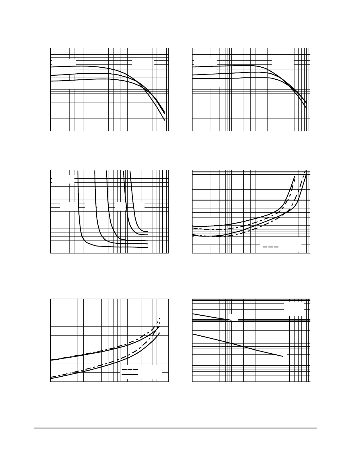
TYPICAL STATIC CHARACTERISTICS
100
, DC CURRENT GAIN
FE
h
10
1
0.01
2
1.5
1
TJ = 125°C
TJ = 25°C
TJ = -20°C
0.1
IC, COLLECTOR CURRENT (AMPS)
Figure 1. DC Current Gain @ 1 Volt
TJ = 25°C
IC = 1 A 3 A 5 A 6 A
2 A
100
VCE = 1 V
110
TJ = 125°C
TJ = 25°C
TJ = -20°C
10
, DC CURRENT GAIN
FE
h
1
0.01 0.1 1 10
10
1
VCE = 5 V
IC, COLLECTOR CURRENT (AMPS)
Figure 2. DC Current Gain @ 5 Volts
, VOLTAGE (VOLTS)
V
, VOLTAGE (VOLTS)
V
CE
BE
0.5
1.3
1.2
1.1
0.9
0.8
0.7
0.6
0.5
0.4
0
0.01
1
0.01
IC/IB = 10
, VOLTAGE (VOLTS)
0.1
CE
V
0.1 1 10
IB, BASE CURRENT (AMPS)
0.01
0.01
IC/IB = 5
0.1
IC COLLECTOR CURRENT (AMPS)
TJ = 25°C
TJ = 125°C
110
Figure 3. Collector Saturation Region Figure 4. Collector−Emitter Saturation Voltage
10000
C
ib
C
10
100
TJ = 25°C
TJ = 125°C
IC/IB = 5
IC/IB = 10
0.1 1 10
IC, COLLECTOR CURRENT (AMPS)
1000
100
10
C, CAPACITANCE (pF)
1
1 1000
VCE, COLLECTOR-EMITTER VOLTAGE (VOLTS)
TJ = 25°C
f = 1 MHz
ob
Figure 5. Base−Emitter Saturation Region Figure 6. Capacitance
http://onsemi.com
3
Page 4

MJE18006G
TYPICAL SWITCHING CHARACTERISTICS
(IB2 = IC/2 for all switching)
2000
I
= IC/2
t, TIME (ns)
1500
1000
B(off)
VCC = 300 V
PW = 20 ms
IC/IB = 5
IC/IB = 10
TJ = 125°C
TJ = 25°C
500
0
0
1350 35
2
46
IC, COLLECTOR CURRENT (AMPS)
Figure 7. Resistive Switching, t
on
3500
I
= IC/2
3000
IC/IB = 5
B(off)
VCC = 15 V
VZ = 300 V
2500
LC = 200 mH
2000
1500
t, TIME (ns)
1000
500
0
034
TJ = 25°C
TJ = 125°C
1
IC/IB = 10
256
IC COLLECTOR CURRENT (AMPS)
4000
3500
3000
2500
2000
t, TIME (ns)
1500
1000
500
0
5000
4500
4000
3500
3000
2500
2000
, STORAGE TIME (ns)
1500
si
t
1000
500
0
IC/IB = 5
TJ = 25°C
TJ = 125°C
IC/IB = 10
1
462
IC, COLLECTOR CURRENT (AMPS)
Figure 8. Resistive Switching, t
TJ = 25°C
TJ = 125°C
IC = 3 A
3
4 5 7 8 10 11 13 14
6
hFE, FORCED GAIN
9
I
= IC/2
B(off)
VCC = 300 V
PW = 20 ms
off
I
= IC/2
B(off)
VCC = 15 V
VZ = 300 V
LC = 200 mH
IC = 1.3 A
12 15
Figure 9. Inductive Storage Time, t
si
350
300
t
c
250
t, TIME (ns)
200
150
100
I
B(off)
= IC/2
t
fi
VCC = 15 V
50
VZ = 300 V
LC = 200 mH
0
0235
11
TJ = 25°C
TJ = 125°C
46
IC, COLLECTOR CURRENT (AMPS)
Figure 11. Inductive Switching, t
and t
c
IC/IB = 5
http://onsemi.com
Figure 10. Inductive Storage Time, tsi(hFE)
250
200
I
= IC/2
B(off)
VCC = 15 V
150
VZ = 300 V
LC = 200 mH
t, TIME (ns)
100
TJ = 25°C
50
TJ = 125°C
IC, COLLECTOR CURRENT (AMPS)
fi
Figure 12. Inductive Switching, t
t
c
t
fi
460235
and t
c
fi
IC/IB = 10
4
Page 5
MJE18006G
TYPICAL SWITCHING CHARACTERISTICS
(IB2 = IC/2 for all switching)
180
160
140
120
, FALL TIME (ns)
fi
100
t
80
60
3
100
10
1
350
300
IC = 3 A
IC = 1.3 A
TJ = 25°C
T
= 125°C
J
515
4 67891011121314
hFE, FORCED GAIN
Figure 13. Inductive Fall Time
I
= IC/2
B(off)
V
= 15 V
CC
= 300 V
V
Z
LC = 200 mH
250
200
150
, CROSSOVER TIME (ns)
C
T
100
IC = 1.3 A
TJ = 25°C
50
35 154 6 7 8 91011121314
TJ = 125°C
Figure 14. Inductive Crossover Time
GUARANTEED SAFE OPERATING AREA INFORMATION
DC (MJE18006)
5 ms
1 ms
10 ms 1 ms
EXTENDED
SOA
1,0
0,8
0,6
0,4
IC = 3 A
hFE, FORCED GAIN
I
= IC/2
B(off)
VCC = 15 V
V
= 300 V
Z
= 200 mH
L
C
SECOND BREAKDOWN
DERATING
0.1
, COLLECTOR CURRENT (AMPS)
C
I
0.01
10
VCE, COLLECTOR-EMITTER VOLTAGE (VOLTS)
100 1000
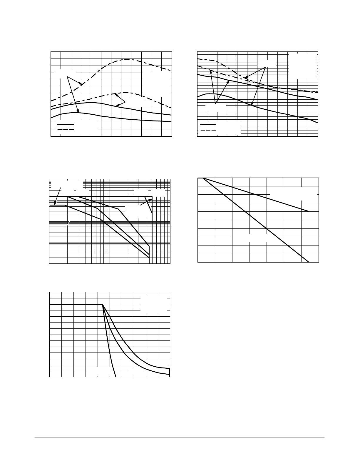
Figure 15. Forward Bias Safe Operating Area
7
TC ≤ 125°C
IC/I
6
5
4
3
2
, COLLECTOR CURRENT (AMPS)
C
1
I
0
0 200
V
= 0 V
BE(off)
400
VCE, COLLECTOR-EMITTER VOLTAGE (VOLTS)
-1, 5 V
600 1000
≥ 4
B
LC = 500 mH
-5 V
800
Figure 16. Reverse Bias Switching Safe Operating Area
There are two limitations on the power handling ability
of a transistor: average junction temperature and second
breakdown. Safe operating area curves indicate IC − V
CE
limits of the transistor that must be observed for reliable
POWER DERATING FACTOR
0,2
0,0
20
40 60 100 120
THERMAL DERATING
80 140 160
TC, CASE TEMPERATURE (°C)
Figure 17. Forward Bias Power Derating
operation; i.e., the transistor must not be subjected to greater
dissipation than the curves indicate. The data of Figure 15 is
based on TC = 25°C; T
is variable depending on power
J(pk)
level. Second breakdown pulse limits are valid for duty
cycles to 10% but must be derated when TC ≥ 25°C. Second
breakdown limitations do not derate the same as thermal
limitations. Allowable current at the voltages shown in
Figure 15 may be found at any case temperature by using the
appropriate curve on Figure 17. T
may be calculated
J(pk)
from the data in Figure 20. At any case temperatures, thermal
limitations will reduce the power that can be handled to
values less than the limitations imposed by second
breakdown. For inductive loads, high voltage and current
must be sustained simultaneously during turn−off with the
base−to−emitter junction reverse−biased. The safe level is
specified as a reverse−biased safe operating area (Figure 16).
This rating is verified under clamped conditions so that the
device is never subjected to an avalanche mode.
http://onsemi.com
5
Page 6
MJE18006G
5
V
CE
4
3
2
dyn 1 ms
dyn 3 ms
1
0
VOLTS
-1
-2
-3
-4
-5
012345678
90% I
B
1 ms
I
B
3 ms
TIME
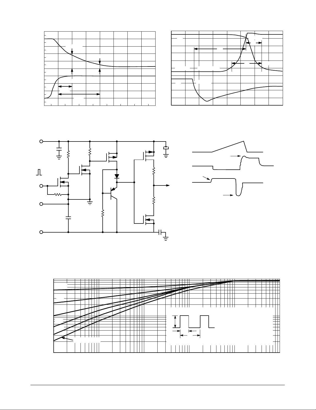
Figure 18. Dynamic Saturation Voltage Measurements
+15 V
150 W
3 W
MTP8P10
MTP8P10
MUR105
MJE210
MTP12N10
+10 V
COMMON
-V
off
1 mF
MPF930
50 W
150 W
3 W
MPF930
500 mF
100 W
3 W
10
I
9
C
8
7
t
si
6
5
V
CLAMP
10% V
CLAMP
90% I
C
t
fi
t
c
4
I
B
3
90% IB1
2
1
0
012 34567 8
TIME
Figure 19. Inductive Switching Measurements
IC PEAK
100 mF
VCE PEAK
V
R
B1
I
out
A
R
B2
1 mF
CE
IB1
I
B
V(BR)CEO(sus)
L = 10 mH
RB2 = ∞
VCC = 20 VOLTS
IC(pk) = 100 mA
IB2
INDUCTIVE SWITCHING
L = 200 mH
RB2 = 0
VCC = 15 VOLTS
RB1 SELECTED FOR
DESIRED IB1
RBSOA
L = 500 mH
RB2 = 0
VCC = 15 VOLTS
RB1 SELECTED
FOR DESIRED IB1
10% I
C
0.1
(NORMALIZED)
r(t), TRANSIENT THERMAL RESISTANCE
0.01
Table 1. Inductive Load Switching Drive Circuit
TYPICAL THERMAL RESPONSE
1
D = 0.5
0.2
0.1
0.05
0.02
SINGLE PULSE
0.01 0.1 1 10 100 1000
Figure 20. Typical Thermal Response (Z
http://onsemi.com
P
t, TIME (ms)
6
(pk)
t
1
t
2
DUTY CYCLE, D = t1/t
(t)) for MJE18006
q
JC
R
(t) = r(t) R
q
JC
R
q
JC
q
JC
= 1.25°C/W MAX
D CURVES APPLY FOR POWER
PULSE TRAIN SHOWN
READ TIME AT t
T
- TC = P
J(pk)
2
(pk)
1
R
(t)
q
JC
Page 7
MJE18006G
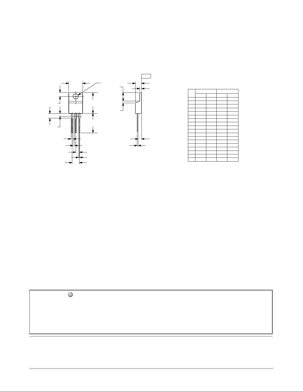
PACKAGE DIMENSIONS
TO−220AB
CASE 221A−09
ISSUE AF
NOTES:
1. DIMENSIONING AND TOLERANCING PER ANSI
SEATING
−T−
PLANE
B
4
Q
123
F
T
A
U
C
S
H
K
Z
L
V
R
J
G
D
N
Y14.5M, 1982.
2. CONTROLLING DIMENSION: INCH.
3. DIMENSION Z DEFINES A ZONE WHERE ALL
BODY AND LEAD IRREGULARITIES ARE
ALLOWED.
DIM MIN MAX MIN MAX
A 0.570 0.620 14.48 15.75
B 0.380 0.405 9.66 10.28
C 0.160 0.190 4.07 4.82
D 0.025 0.035 0.64 0.88
F 0.142 0.161 3.61 4.09
G 0.095 0.105 2.42 2.66
H 0.110 0.155 2.80 3.93
J 0.014 0.025 0.36 0.64
K 0.500 0.562 12.70 14.27
L 0.045 0.060 1.15 1.52
N 0.190 0.210 4.83 5.33
Q 0.100 0.120 2.54 3.04
R 0.080 0.110 2.04 2.79
S 0.045 0.055 1.15 1.39
T 0.235 0.255 5.97 6.47
U 0.000 0.050 0.00 1.27
V 0.045 --- 1.15 ---
Z --- 0.080 --- 2.04
STYLE 1:
PIN 1. BASE
2. COLLECTOR
3. EMITTER
4. COLLECTOR
MILLIMETERSINCHES
SWITCHMODE is a trademark of Semiconductor Components Industries, LLC.
ON Semiconductor and are registered trademarks of Semiconductor Components Industries, LLC (SCILLC). SCILLC reserves the right to make changes without further notice
to any products herein. SCILLC makes no warranty, representation or guarantee regarding the suitability of its products for any particular purpose, nor does SCILLC assume any liability
arising out of the application or use of any product or circuit, and specifically disclaims any and all liability, including without limitation special, consequential or incidental damages.
“Typical” parameters which may be provided in SCILLC data sheets and/or specifications can and do vary in different applications and actual performance may vary over time. All
operating parameters, including “Typicals” must be validated for each customer application by customer’s technical experts. SCILLC does not convey any license under its patent rights
nor the rights of others. SCILLC products are not designed, intended, or authorized for use as components in systems intended for surgical implant into the body, or other applications
intended to support or sustain life, or for any other application in which the failure of the SCILLC product could create a situation where personal injury or death may occur. Should
Buyer purchase or use SCILLC products for any such unintended or unauthorized application, Buyer shall indemnify and hold SCILLC and its officers, employees, subsidiaries, affiliates,
and distributors harmless against all claims, costs, damages, and expenses, and reasonable attorney fees arising out of, directly or indirectly, any claim of personal injury or death
associated with such unintended or unauthorized use, even if such claim alleges that SCILLC was negligent regarding the design or manufacture of the part. SCILLC is an Equal
Opportunity/Affirmative Action Employer. This literature is subject to all applicable copyright laws and is not for resale in any manner.
PUBLICATION ORDERING INFORMATION
LITERATURE FULFILLMENT:
Literature Distribution Center for ON Semiconductor
P.O. Box 5163, Denver, Colorado 80217 USA
Phone: 303−675−2175 or 800−344−3860 Toll Free USA/Canada
Fax: 303−675−2176 or 800−344−3867 Toll Free USA/Canada
Email: [email protected]
N. American Technical Support: 800−282−9855 Toll Free
USA/Canada
Europe, Middle East and Africa Technical Support:
Phone: 421 33 790 2910
Japan Customer Focus Center
Phone: 81−3−5773−3850
http://onsemi.com
ON Semiconductor Website: www.onsemi.com
Order Literature: http://www.onsemi.com/orderlit
For additional information, please contact your local
Sales Representative
MJE18006/D
7
 Loading...