

Page 1
1
Motorola Bipolar Power Transistor Device Data
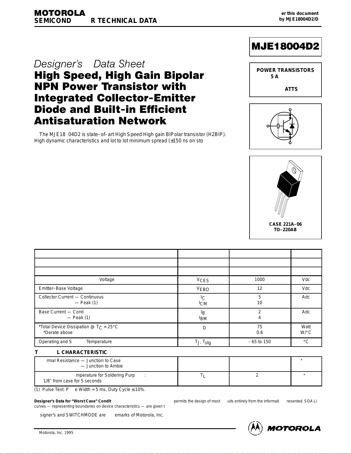
! ' ! !% !'&#(
&,( (%)!)*&( ,!*
%*(* &##*&($!**(
!& % +!#*!% !!%*
%*!)*+(*!&% *,&("
The MJE18004D2 is state–of–art High Speed High gain BIPolar transistor (H2BIP).
High dynamic characteristics and lot to lot minimum spread (±150 ns on storage time)
make it ideally suitable for light ballast applications. Therefore, there is no need to
guarantee an hFE window.
Main features:
• Low Base Drive Requirement
• High Peak DC Current Gain (55 Typical) @ IC = 100 mA
• Extremely Low Storage Time Min/Max Guarantees Due to the
H2BIP Structure which Minimizes the Spread
• Integrated Collector–Emitter Free Wheeling Diode
• Fully Characterized and Guaranteed Dynamic V
CE(sat)
• “6 Sigma” Process Providing Tight and Reproductible Parameter Spreads
It’s characteristics make it also suitable for PFC application.
MAXIMUM RATINGS
Rating
Symbol
ОООООООО
ОООООООО
ОООООООО
Value
ÎÎÎÎ
ÎÎÎÎ
ÎÎÎÎ
Unit
Collector–Emitter Sustaining Voltage
V
CEO
ОООООООО
ОООООООО
ОООООООО
450
ÎÎÎÎ
ÎÎÎÎ
ÎÎÎÎ
Vdc
Collector–Base Breakdown Voltage
V
CBO
ОООООООО
ОООООООО
ОООООООО
1000
ÎÎÎÎ
ÎÎÎÎ
ÎÎÎÎ
Vdc
Collector–Emitter Breakdown Voltage
V
CES
ОООООООО
ОООООООО
ОООООООО
1000
ÎÎÎÎ
ÎÎÎÎ
ÎÎÎÎ
Vdc
Emitter–Base Voltage
V
EBO
ОООООООО
ОООООООО
ОООООООО
12
ÎÎÎÎ
ÎÎÎÎ
ÎÎÎÎ
Vdc
Collector Current — Continuous
Collector Current — Peak (1)
I
C
I
CM
ОООООООО
ОООООООО
ОООООООО
ОООООООО
5
10
ÎÎÎÎ
ÎÎÎÎ
ÎÎÎÎ
ÎÎÎÎ
Adc
Base Current — Continuous
Base Current — Peak (1)
I
B
I
BM
ОООООООО
ОООООООО
ОООООООО
2
4
ÎÎÎÎ
ÎÎÎÎ
ÎÎÎÎ
Adc
*Total Device Dissipation @ TC = 25_C
*Derate above 25°C
P
D
ОООООООО
ОООООООО
ОООООООО
ОООООООО
75
0.6
ÎÎÎÎ
ÎÎÎÎ
ÎÎÎÎ
ÎÎÎÎ
Watt
W/_C
Operating and Storage Temperature
TJ, T
stg
ОООООООО
ОООООООО
ОООООООО
–65 to 150
ÎÎÎÎ
ÎÎÎÎ
ÎÎÎÎ
_
C
THERMAL CHARACTERISTICS
Thermal Resistance — Junction to Case
Thermal Resistance — Junction to Ambient
R
θJC
R
θJA
ОООООООО
ОООООООО
ОООООООО
ОООООООО
1.65
62.5
ÎÎÎÎ
ÎÎÎÎ
ÎÎÎÎ
ÎÎÎÎ
_
C/W
Maximum Lead Temperature for Soldering Purposes:
1/8″ from case for 5 seconds
T
L
ОООООООО
ОООООООО
ОООООООО
260
ÎÎÎÎ
ÎÎÎÎ
ÎÎÎÎ
_
C
(1) Pulse Test: Pulse Width = 5 ms, Duty Cycle ≤ 10%.
Designer’s Data for “Worst Case” Conditions — The Designer’s Data Sheet permits the design of most circuits entirely from the information presented. SOA Limit
curves — representing boundaries on device characteristics — are given to facilitate “worst case” design.
Designer’s and SWITCHMODE are trademarks of Motorola, Inc.
SEMICONDUCTOR TECHNICAL DATA
Order this document
by MJE18004D2/D
Motorola, Inc. 1995
POWER TRANSISTORS
5 AMPERES
1000 VOLTS
75 WATTS
CASE 221A–06
TO–220AB
Page 2
MJE18004D2
2
Motorola Bipolar Power Transistor Device Data
ELECTRICAL CHARACTERISTICS
(T
C
= 25°C unless otherwise noted)
Characteristic
Symbol
Min
Typ
Max
Unit
OFF CHARACTERISTICS
Collector–Emitter Sustaining Voltage
(IC = 100 mA, L = 25 mH)
V
CEO(sus)
450
547
Vdc
Collector–Base Breakdown Voltage
(I
CBO
= 1 mA)
V
CBO
1000
1100
Vdc
Emitter–Base Breakdown Voltage
(I
EBO
= 1 mA)
V
EBO
12
14
Vdc
Collector Cutoff Current
(VCE = Rated V
CEO
, IB = 0)
I
CEO
100
µAdc
Collector Cutoff Current (VCE = Rated V
CES
, VEB = 0)
Collector Cutoff Current (VCE = 500 V, VEB = 0)
@ TC = 25°C
@ TC = 125°C
@ TC = 125°C
I
CES
100
500
100
µAdc
Emitter–Cutoff Current
(VEB = 10 Vdc, IC = 0)
I
EBO
100
µAdc
ON CHARACTERISTICS
Base–Emitter Saturation Voltage
(IC = 0.8 Adc, IB = 80 mAdc)
@ TC = 25°C
@ TC = 125°C
0.8
0.7
1
0.9
(IC = 2 Adc, IB = 0.4 Adc)
@ TC = 25°C
@ TC = 125°C
0.9
0.8
1
0.9
Collector–Emitter Saturation Voltage
(IC = 0.8 Adc, IB = 80 mAdc)
@ TC = 25°C
@ TC = 125°C
0.38
0.55
0.5
0.75
(IC = 2 Adc, IB = 0.4 Adc)
@ TC = 25°C
@ TC = 125°C
0.45
0.75
0.75
1
(IC = 0.8 Adc, IB = 40 mAdc)
@ TC = 25°C
@ TC = 125°C
0.9
1.6
1.5
(IC = 1 Adc, IB = 0.2 Adc)
@ TC = 25°C
@ TC = 125°C
0.25
0.28
0.5
0.6
DC Current Gain
(IC = 0.8 Adc, VCE = 1 Vdc)
@ TC = 25°C
@ TC = 125°C
15
10
28
14
(IC = 2 Adc, VCE = 1 Vdc)
@ TC = 25°C
@ TC = 125°C
6
4
8
6
(IC = 1 Adc, VCE = 2.5 Vdc)
@ TC = 25°C
@ TC = 125°C
18
14
28
20
DYNAMIC SATURATION VOLTAGE
@ 1 µs
@ TC = 25°C
@ TC = 125°C
9
16
Dynamic Saturation
Voltage:
Determined 1 µs and
IB1 = 100 mA
VCC = 300 V
@ 3 µs
@ TC = 25°C
@ TC = 125°C
3.1
9
µs and
3 µs respectively after
rising IB1 reaches
@ 1 µs
@ TC = 25°C
@ TC = 125°C
11
18
90% of final I
B1
IB1 = 0.4 A
VCC = 300 V
@ 3 µs
@ TC = 25°C
@ TC = 125°C
1.4
8
V
BE(sat)
Vdc
IC = 1 Adc
IC = 2 Adc
V
CE(sat)
h
FE
V
CE(dsat)
Vdc
—
V
Page 3
MJE18004D2
3
Motorola Bipolar Power Transistor Device Data
ELECTRICAL CHARACTERISTICS (T
C
= 25°C unless otherwise noted)
Characteristic
Symbol
Min
ÎÎÎ
ÎÎÎ
ÎÎÎ
Typ
Max
Unit
DIODE CHARACTERISTICS
Forward Diode Voltage
(IEC = 1 Adc)
@ TC = 25°C
@ TC = 125°C
ÎÎÎ
ÎÎÎ
ÎÎÎ
ÎÎÎ
ÎÎÎ
0.96
0.72
1.5
(IEC = 2 Adc)
@ TC = 25°C
@ TC = 125°C
ÎÎÎ
ÎÎÎ
ÎÎÎ
1.15
0.8
1.7
Forward Recovery Time
(IF = 0.4 Adc, di/dt = 10 A/µs)
@ TC = 25°C
ÎÎÎ
ÎÎÎ
ÎÎÎ
ÎÎÎ
440
(IF = 1 Adc, di/dt = 10 A/µs)
@ TC = 25°C
ÎÎÎ
ÎÎÎ
ÎÎÎ
335
(IF = 2 Adc, di/dt = 10 A/µs)
@ TC = 25°C
ÎÎÎ
ÎÎÎ
ÎÎÎ
335
DYNAMIC CHARACTERISTICS
Current Gain Bandwidth
(IC = 0.5 Adc, VCE = 10 Vdc, f = 1 MHz)
f
T
ÎÎÎ
ÎÎÎ
ÎÎÎ
ÎÎÎ
13
MHz
Output Capacitance
(VCB = 10 Vdc, IE = 0, f = 1 MHz)
C
ob
ÎÎÎ
ÎÎÎ
ÎÎÎ
60
100
pF
Input Capacitance
(IC = 0.5 Adc, VCE = 10 Vdc, f = 1 MHz)
C
ib
ÎÎÎ
ÎÎÎ
ÎÎÎ
ÎÎÎ
450
750
pF
SWITCHING CHARACTERISTICS: Resistive Load (D.C. ≤ 10%, Pulse Width = 40 µs)
Turn–on Time
@ TC = 25°C
t
on
ÎÎÎ
ÎÎÎ
ÎÎÎ
500
750
ns
Turn–off Time
IB2 = 1 Adc
VCC = 250 Vdc
@ TC = 25°C
t
off
1.1
ÎÎÎ
ÎÎÎ
ÎÎÎ
1.4
µs
Turn–on Time
@ TC = 25°C
@ TC = 125°C
t
on
ÎÎÎ
ÎÎÎ
ÎÎÎ
ÎÎÎ
100
150
150
ns
Turn–off Time
IB2 = 1 Adc
VCC = 300 Vdc
@ TC = 25°C
@ TC = 125°C
t
off
ÎÎÎ
ÎÎÎ
ÎÎÎ
ÎÎÎ
1.15
1.6
1.3
µs
Turn–on Time
@ TC = 25°C
@ TC = 125°C
t
on
ÎÎÎ
ÎÎÎ
ÎÎÎ
120
500
150
ns
Turn–off Time
IB2 = 0.5 Adc
VCC = 300 Vdc
@ TC = 25°C
@ TC = 125°C
t
off
1.85
ÎÎÎ
ÎÎÎ
ÎÎÎ
ÎÎÎ
2.6
2.15
µs
SWITCHING CHARACTERISTICS: Inductive Load (VCC = 15 V)
Fall Time
@ TC = 25°C
@ TC = 125°C
t
f
ÎÎÎ
ÎÎÎ
ÎÎÎ
ÎÎÎ
130
300
175
ns
Storage Time
C
= 2.5 Adc
IB1 = 500 mAdc
IB2 = 500 mAdc
V
= 350 V
@ TC = 25°C
@ TC = 125°C
t
s
ÎÎÎ
ÎÎÎ
ÎÎÎ
2.12
2.6
2.4
µs
Crossover Time
VZ = 350 V
LC = 300 µH
@ TC = 25°C
@ TC = 125°C
t
c
ÎÎÎ
ÎÎÎ
ÎÎÎ
ÎÎÎ
355
750
500
ns
Fall Time
@ TC = 25°C
@ TC = 125°C
t
f
ÎÎÎ
ÎÎÎ
ÎÎÎ
ÎÎÎ
95
230
150
ns
Storage Time
C
= 2 Adc
IB1 = 400 mAdc
IB2 = 400 mAdc
V
= 300 V
@ TC = 25°C
@ TC = 125°C
t
s
2.1
ÎÎÎ
ÎÎÎ
ÎÎÎ
2.9
2.4
µs
Crossover Time
VZ = 300 V
LC = 200 µH
@ TC = 25°C
@ TC = 125°C
t
c
ÎÎÎ
ÎÎÎ
ÎÎÎ
ÎÎÎ
300
700
450
ns
Fall Time
@ TC = 25°C
@ TC = 125°C
t
f
ÎÎÎ
ÎÎÎ
ÎÎÎ
ÎÎÎ
70
100
90
ns
Storage Time
C
= 1 Adc
IB1 = 100 mAdc
IB2 = 500 mAdc
V
= 300 V
@ TC = 25°C
@ TC = 125°C
t
s
ÎÎÎ
ÎÎÎ
ÎÎÎ
0.7
1.05
0.9
µs
Crossover Time
VZ = 300 V
LC = 200 µH
@ TC = 25°C
@ TC = 125°C
t
c
ÎÎÎ
ÎÎÎ
ÎÎÎ
ÎÎÎ
75
160
120
ns
V
EC
t
fr
IC = 2.5 Adc, IB1 = 0.5 Adc
IC = 2 Adc, IB1 = 0.4 Adc
IC = 2.5 Adc, IB1 = 0.5 Adc
IC = 2.5 Adc
IC = 2 Adc
IC = 1 Adc
V
ns
Page 4
MJE18004D2
4
Motorola Bipolar Power Transistor Device Data
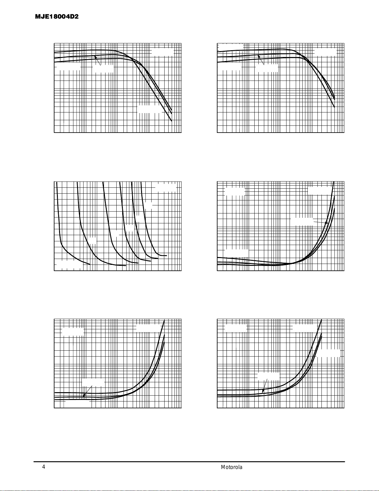
TYPICAL STATIC CHARACTERISTICS
Figure 1. DC Current Gain @ 1 Volt
100
10
1
1010.10.010.001
IC, COLLECTOR CURRENT (AMPS)
h
FE
, DC CURRENT GAIN
TJ = 125°C
TJ = 25°C
TJ = –20°C
VCE = 1 V
Figure 2. DC Current Gain @ 5 Volt
100
10
1
1010.10.010.001
IC, COLLECTOR CURRENT (AMPS)
h
FE
, DC CURRENT GAIN
TJ = 125°C
TJ = –20°C
VCE = 5 V
Figure 3. Collector Saturation Region
3
2
0
1010.10.01
IB, BASE CURRENT (mA)
IC = 500 mA
Figure 4. Collector–Emitter Saturation Voltage
10
1
0.1
1010.10.010.001
IC, COLLECTOR CURRENT (AMPS)
TJ = 125
°
C
TJ = 25°C
TJ = –20°C
IC/IB = 5
V
CE
, VOLTAGE (VOLTS)
V
CE
, VOLTAGE (VOLTS)
1
TJ = 25°C
1 A
5 A
Figure 5. Collector–Emitter Saturation Voltage
10
1
0.1
100.10.010.001
IC, COLLECTOR CURRENT (AMPS)
Figure 6. Collector–Emitter Saturation Voltage
10
1
0.1
100.10.010.001
IC, COLLECTOR CURRENT (AMPS)
TJ = 125
°
C
TJ = –20°C
V
CE
, VOLTAGE (VOLTS)
V
CE
, VOLTAGE (VOLTS)
1
IC/IB = 10
TJ = 125°C
TJ = –20°C
IC/IB = 20
4 A
3 A
2 A
TJ = 25°C
TJ = 25°C
TJ = 25°C
1
Page 5

MJE18004D2
5
Motorola Bipolar Power Transistor Device Data
TYPICAL STATIC CHARACTERISTICS
Figure 7. Base–Emitter Saturation Region
10
1
0.1
100.10.010.001
IC, COLLECTOR CURRENT (AMPS)
Figure 8. Base–Emitter Saturation Region
10
1
0.1
100.10.010.001
IC, COLLECTOR CURRENT (AMPS)
TJ = 125
°
C
TJ = –20°C
V
BE
, VOLTAGE (VOLTS)
V
BE
, VOLTAGE (VOLTS)
1
TJ = 125°C
TJ = 25°C
TJ = –20°C
IC/IB = 10
1
IC/IB = 5
Figure 9. Base–Emitter Saturation Region
10
1
0.1
100.10.010.001
IC, COLLECTOR CURRENT (AMPS)
Figure 10. Forward Diode Voltage
10
1
0.1
100.10.01
REVERSE EMITTER–COLLECTOR CURRENT (AMPS)
125
°
C
25°C
V
BE
, VOLTAGE (VOLTS)
FORWARD DIODE VOLTAGE (VOLTS)
TJ = 125°C
TJ = –20°C
1
IC/IB = 20
Figure 11. Capacitance
1000
10
100101
VR, REVERSE VOLTAGE (VOLTS)
C, CAPACITANCE (pF)
100
Cib (pF)
C
ob
TJ = 25°C
f
(test)
= 1 MHz
Figure 12. BVCER = f(RBE)
1200
600
100010010
BASE–EMITTER RESISTOR (
Ω
)
COLLECTOR EMITTER VOLTAGE (VOLTS)
TC = 25°C
BVCER @ ICER = 10 mA
1000
800
BVCER(sus) @
ICER = 200 mA,
Lc = 25 mH
1
TJ = 25°C
TJ = 25°C
Page 6

MJE18004D2
6
Motorola Bipolar Power Transistor Device Data
TYPICAL SWITCHING CHARACTERISTICS
Figure 13. Resistive Switch Time, t
on
3200
0
4
2
1
IC, COLLECTOR CURRENT (AMPS)
3
t, TIME (ns)
2400
1600
800
TJ = 125°C
TJ = 25
°
C
IC/IB = 10
IC/IB = 5
I
Bon
= I
Boff
VCC = 300 V
PW = 20 µs
Figure 14. Resistive Switch Time, t
off
5
2
0
431
IC, COLLECTOR CURRENT (AMPS)
Figure 15. Inductive Storage Time,
tsi @ IC/IB = 5
4
2
0
410
IC, COLLECTOR CURRENT (AMPS)
3
3
1
3
t, TIME ( s)
µ
t, TIME ( s)
µ
4
1
TJ = 125°C
TJ = 25
°
C
IC/IB = 10
IC/IB = 5
I
Bon
= I
Boff
VCC = 300 V
PW = 20 µs
2
TJ = 125°C
TJ = 25
°
C
I
Bon
= I
Boff
VCC = 15 V
VZ = 300 V
LC = 200
µ
H
Figure 16. Inductive Storage Time,
tsi @ IC/IB = 10
2
IC/IB = 5
4
2
0
410
IC, COLLECTOR CURRENT (AMPS)
3
3
1
t, TIME ( s)
µ
2
TJ = 125°C
TJ = 25
°
C
I
Bon
= I
Boff
VCC = 15 V
VZ = 300 V
LC = 200
µ
H
IC/IB = 10
Figure 17. Inductive Switching Time,
tc & tfi @ IC/IB = 5
1000
0
410
IC, COLLECTOR CURRENT (AMPS)
3
t, TIME (ns)
800
600
200
TJ = 125°C
TJ = 25
°
C
400
2
I
Bon
= I
Boff
VCC = 15 V
VZ = 300 V
LC = 200
µ
H
IC/IB = 5
Figure 18. Inductive Switching Time,
tfi @ IC/IB = 10
1000
0
410
IC, COLLECTOR CURRENT (AMPS)
3
t, TIME (ns)
800
600
200
TJ = 125°C
TJ = 25
°
C
400
2
I
Boff
= I
Bon
VCC = 15 V
VZ = 300 V
LC = 200
µ
H
IC/IB = 10
t
c
t
fi
Page 7

MJE18004D2
7
Motorola Bipolar Power Transistor Device Data
, STORAGE TIME (t
si
µ
s)
TYPICAL SWITCHING CHARACTERISTICS
Figure 19. Inductive Switching, tc @ IC/IB = 10
1600
800
0
420
IC, COLLECTOR CURRENT (AMPS)
t, TIME (ns)
1200
TJ = 125°C
TJ = 25
°
C
400
1 3
IC/IB = 10
I
Boff
= I
Bon
VCC = 15 V
VZ = 300 V
LC = 200
µ
H
Figure 20. Inductive Storage Time
5
2
200
hFE, FORCED GAIN
4
3
5 10 15
TJ = 125°C
TJ = 25
°
C
IC = 2 A
I
Bon
= I
Boff
VCC = 15 V
VZ = 300 V
LC = 200
µ
H
IC = 1 A
Figure 21. Inductive Fall Time
1000
0
2082
hFE, FORCED GAIN
Figure 22. Inductive Crossover Time
2000
500
0
2082
hFE, FORCED GAIN
1500
1000
600
t
fi
, FALL TIME (ns)
t
c
, CROSSOVER TIME (ns)
800
400
200
4 6 10 12
TJ = 125°C
TJ = 25
°
C
I
Boff
= I
Bon
VCC = 15 V
VZ = 300 V
LC = 200
µ
H
14
I
Bon
= I
Boff
VCC = 15 V
VZ = 300 V
LC = 200
µ
H
TJ = 125°C
TJ = 25
°
C
14 16 18
IC = 1 A
IC = 2 A
IC = 2 A
IC = 1 A
Figure 23. Inductive Storage Time, t
si
4
2
1
40.5
IC, COLLECTOR CURRENT (AMPS)
1.51
I
Bon
= I
Boff
VCC = 15 V
VZ = 300 V
LC = 200
µ
H
3
t, TIME ( s)
µ
2 2.5 3 3.5
IB = 50 mA
IB = 100 mA
IB = 200 mA
IB = 500 mA
IB = 1 A
Figure 24. Forward Recovery Time, T
FR
420
300
210.50
IF, FORWARD CURRENT (AMP)
dI/dt = 10 A/µs
TC = 25
°
C
1.5
t
fr
, FORWARD RECOVERY TIME (ns)
380
340
Page 8

MJE18004D2
8
Motorola Bipolar Power Transistor Device Data
10
4
0
820 6
8
6
2
4
9
7
5
3
1
1 3 5
7
I
B
I
C
V
clamp
t
si
t
c
t
fi
90% I
C
10% I
C
90% I
B1
10% V
clamp
V
CE
0 V
I
B
90% I
B
1 µs
3 µs
dyn 1 µs
dyn 3 µs
Figure 25. Dynamic Saturation
Voltage Measurements
TIME
VOLTS
Figure 26. Inductive Switching Measurements
TYPICAL SWITCHING CHARACTERISTICS
Figure 27. tfr Measurements
0
1060
V
F
I
F
2 84
VFR (1.1 VF unless otherwise specified)
V
FRM
t
fr
V
F
0.1 V
F
10% I
F
TIME
Page 9

MJE18004D2
9
Motorola Bipolar Power Transistor Device Data
TYPICAL SWITCHING CHARACTERISTICS
Table 1. Inductive Load Switching Drive Circuit
V
(BR)CEO(sus)
L = 10 mH
RB2 =
∞
VCC = 20 Volts
I
C(pk)
= 100 mA
Inductive Switching
L = 200
µ
H
RB2 = 0
VCC = 15 Volts
RB1 selected for
desired Ib1
RBSOA
L = 500
µ
H
RB2 = 0
VCC = 15 Volts
RB1 selected for
desired Ib1
+15 V
1
µ
F
150
Ω
3 W
100
Ω
3 W
MPF930
+10 V
50
Ω
COMMON
–V
off
500
µ
F
MPF930
MTP8P10
MUR105
MJE210
MTP12N10
MTP8P10
150
Ω
3 W
100 µF
I
out
A
1
µ
F
R
B2
R
B1
IC PEAK
VCE PEAK
V
CE
I
B
IB1
IB2
TYPICAL CHARACTERISTICS
Figure 28. Forward Bias Safe Operating Area
100
0.01
100010
VCE, COLLECTOR–EMITTER VOLTAGE (VOLTS)
Figure 29. Reverse Bias Safe Operating Area
6
2
0
1000200
VCE, COLLECTOR–EMITTER VOLTAGE (VOLTS)
4
100 600
1
0.1
I
C
, COLLECTOR CURRENT (AMPS)
I
C
, COLLECTOR CURRENT (AMPS)
DC
5 ms
1 ms
10 µs
1 µs
EXTENDED
SOA
3
1
0 V –1.5 V
–5 V
TC ≤ 125°C
GAIN
≥
5
LC = 2 mH
10
5
400 800
Page 10

MJE18004D2
10
Motorola Bipolar Power Transistor Device Data
TYPICAL CHARACTERISTICS
POWER DERATING FACTOR
Figure 30. Forward Bias Power Derating
There are two limitations on the power handling ability of
a transistor: average junction temperature and second
breakdown. Safe operating area curves indicate IC–V
CE
limits of the transistor that must be observed for reliable
operation; i.e., the transistor must not be subjected to
greater dissipation than the curves indicate. The data of
Figure 28 is based on TC = 2 5°C; TJ(pk) i s variable
depending on power level. Second breakdown pulse limits
are valid for duty cycles to 10% but must be derated when
TC > 25°C. Second breakdown limitations do not derate the
same as t hermal l imitations. A llowable current a t the
voltages shown on Figure 28 may be found at any case
temperature by using the appropriate curve on Figure 30.
TJ(pk) may be calculated from the data in Figure 31. At
any case temperatures, thermal limitations will reduce the
power that c an b e handled to v alues less t han the
limitations imposed by second breakdown. For inductive
loads, high voltage and current must be sustained simultaneously during turn–off with the base–to–emitter junction
reverse biased. The safe level is specified as a reverse–
biased safe operating area (Figure 29). This rating is
verified under clamped conditions so that the device is
never subjected to an avalanche mode.
TC, CASE TEMPERATURE (°C)
1.0
0.8
0.6
0.4
0.2
0
16014012010080604020
SECOND
BREAKDOWN
DERATING
THERMAL
DERATING
Figure 31. Typical Thermal Response (Z
θJC(t)
) for MJE18004D2
TYPICAL THERMAL RESPONSE
1
0.01
100.10.01
t, TIME (ms)
0.1
1 100 1000
r(t), TRANSIENT THERMAL RESISTANCE
(NORMALIZED)
R
θ
JC
(t) = r(t) R
θ
JC
R
θ
JC
= 2.5
°
C/W MAX
D CURVES APPLY FOR POWER
PULSE TRAIN SHOWN
READ TIME AT t
1
T
J(pk)
– TC = P
(pk)
R
θ
JC
(t)
P
(pk)
t
1
t
2
DUTY CYCLE, D = t1/t
2
0.05
SINGLE PULSE
0.5
0.2
0.1
0.02
Page 11

MJE18004D2
11
Motorola Bipolar Power Transistor Device Data
PACKAGE DIMENSIONS
CASE 221A–06
TO–220AB
ISSUE Y
NOTES:
1. DIMENSIONING AND TOLERANCING PER ANSI
Y14.5M, 1982.
2. CONTROLLING DIMENSION: INCH.
3. DIMENSION Z DEFINES A ZONE WHERE ALL
BODY AND LEAD IRREGULARITIES ARE
ALLOWED.
STYLE 1:
PIN 1. BASE
2. COLLECTOR
3. EMITTER
4. COLLECTOR
DIM MIN MAX MIN MAX
MILLIMETERSINCHES
A 0.570 0.620 14.48 15.75
B 0.380 0.405 9.66 10.28
C 0.160 0.190 4.07 4.82
D 0.025 0.035 0.64 0.88
F 0.142 0.147 3.61 3.73
G 0.095 0.105 2.42 2.66
H 0.110 0.155 2.80 3.93
J 0.018 0.025 0.46 0.64
K 0.500 0.562 12.70 14.27
L 0.045 0.060 1.15 1.52
N 0.190 0.210 4.83 5.33
Q 0.100 0.120 2.54 3.04
R 0.080 0.110 2.04 2.79
S 0.045 0.055 1.15 1.39
T 0.235 0.255 5.97 6.47
U 0.000 0.050 0.00 1.27
V 0.045 ––– 1.15 –––
Z ––– 0.080 ––– 2.04
B
Q
H
Z
L
V
G
N
A
K
F
1 2 3
4
D
SEATING
PLANE
–T–
C
S
T
U
R
J
Page 12

MJE18004D2
12
Motorola Bipolar Power Transistor Device Data
How to reach us:
USA /EUROPE: Motorola Literature Distribution; JAPAN: Nippon Motorola Ltd.; Tatsumi–SPD–JLDC, Toshikatsu Otsuki,
P.O. Box 20912; Phoenix, Arizona 85036. 1–800–441–2447 6F Seibu–Butsuryu–Center, 3–14–2 Tatsumi Koto–Ku, Tokyo 135, Japan. 03–3521–8315
MFAX: RMFAX0@email.sps.mot.com – TOUCHTONE (602) 244–6609 HONG KONG: Motorola Semiconductors H.K. Ltd.; 8B Tai Ping Industrial Park,
INTERNET: http://Design–NET.com 51 Ting Kok Road, Tai Po, N.T., Hong Kong. 852–26629298
Motorola reserves the right to make changes without further notice to any products herein. Motorola makes no warranty , representation or guarantee regarding
the suitability of its products for any particular purpose, nor does Motorola assume any liability arising out of the application or use of any product or circuit,
and specifically disclaims any and all liability, including without limitation consequential or incidental damages. “T ypical” parameters can and do vary in different
applications. All operating parameters, including “T ypicals” must be validated for each customer application by customer’s technical experts. Motorola does
not convey any license under its patent rights nor the rights of others. Motorola products are not designed, intended, or authorized for use as components in
systems intended for surgical implant into the body, or other applications intended to support or sustain life, or for any other application in which the failure of
the Motorola product could create a situation where personal injury or death may occur. Should Buyer purchase or use Motorola products for any such
unintended or unauthorized application, Buyer shall indemnify and hold Motorola and its officers, employees, subsidiaries, affiliates, and distributors harmless
against all claims, costs, damages, and expenses, and reasonable attorney fees arising out of, directly or indirectly, any claim of personal injury or death
associated with such unintended or unauthorized use, even if such claim alleges that Motorola was negligent regarding the design or manufacture of the part.
Motorola and are registered trademarks of Motorola, Inc. Motorola, Inc. is an Equal Opportunity/Affirmative Action Employer.
MJE18004D2/D
*MJE18004D2/D*
◊
 Loading...