

Page 1
1
Motorola Bipolar Power Transistor Device Data
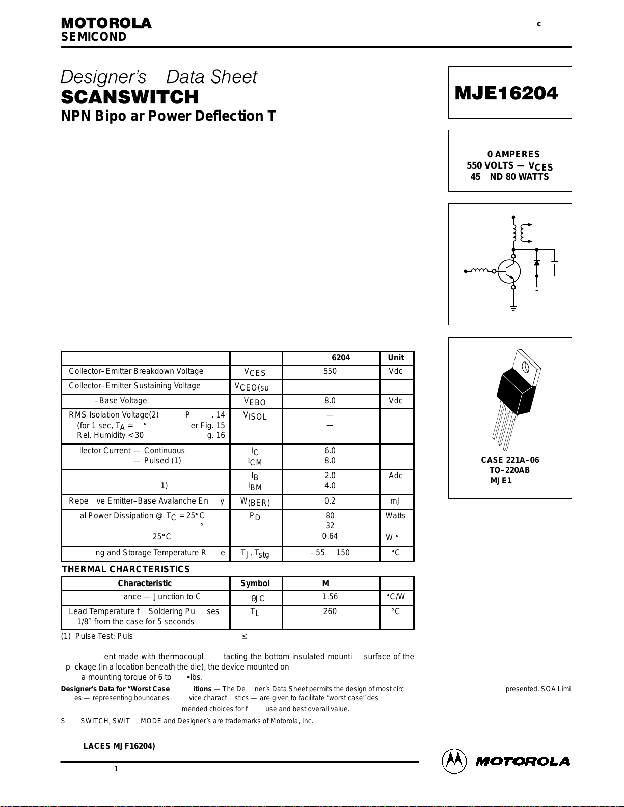
NPN Bipolar Power Deflection Transistor
For High and Very High Resolution Monitors
The MJE16204 is a state–of–the–art SWITCHMODE bipolar power transistor. It is
specifically designed for use in horizontal deflection circuits for 20 mm diameter neck,
high and very resolution, full page, monochrome monitors.
• 550 Volt Collector–Base Breakdown Capability
• Typical Dynamic Desaturation Specified (New Turn–Off Characteristic)
• Application Specific State–of–the–Art Die Design
• Isolated or Non–Isolated TO–220 Type Packages
• Fast Switching:
65 ns Inductive Fall Time (Typ)
680 ns Inductive Storage Time (Typ)
• Low Saturation Voltage:
0.4 Volts at 3.0 Amps Collector Current and 400 mA Base Drive
• Low Collector–Emitter Leakage Current — 100 µA Max at 550 Volts — V
CES
• High Emitter–Base Breakdown Capability For High Voltage Off Drive Circuits —
9.0 Volts (Min)
• Case 221D is UL Recognized at 3500 V
RMS
: File #E69369
MAXIMUM RATINGS
Rating
Symbol
ООООООО
ООООООО
ООООООО
MJE16204
Unit
Collector–Emitter Breakdown Voltage
V
CES
ООООООО
ООООООО
ООООООО
550
Vdc
Collector–Emitter Sustaining Voltage
V
CEO(sus)
ООООООО
ООООООО
ООООООО
250
Vdc
Emitter–Base Voltage
V
EBO
ООООООО
ООООООО
ООООООО
8.0
Vdc
RMS Isolation Voltage(2) Per Fig. 14
(for 1 sec, TA = 25_C, Per Fig. 15
Rel. Humidity < 30%) Per Fig. 16
V
ISOL
ООООООО
ООООООО
ООООООО
ООООООО
—
—
—
V
Collector Current — Continuous
— Pulsed (1)
I
C
I
CM
ООООООО
ООООООО
ООООООО
ООООООО
6.0
8.0
Adc
Base Current — Continuous
— Pulsed (1)
I
B
I
BM
ООООООО
ООООООО
ООООООО
2.0
4.0
Adc
Repetitive Emitter–Base Avalanche Energy
W
(BER)
ООООООО
ООООООО
ООООООО
0.2
mJ
Total Power Dissipation @ TC = 25_C
Total Power Dissipation @ TC = 100_C
Derated above TC = 25_C
P
D
ООООООО
ООООООО
ООООООО
ООООООО
80
32
0.64
Watts
W/_C
Operating and Storage Temperature Range
TJ, T
stg
ООООООО
ООООООО
ООООООО
–55 to 150
_
C
THERMAL CHARCTERISTICS
Characteristic
Symbol
ООООООО
ООООООО
ООООООО
Max
Unit
Thermal Resistance — Junction to Case
R
θJC
ООООООО
ООООООО
ООООООО
1.56
_
C/W
Lead Temperature for Soldering Purposes
1/8″ from the case for 5 seconds
T
L
ООООООО
ООООООО
ООООООО
ООООООО
260
_
C
(1) Pulse Test: Pulse Width = 5.0 ms, Duty Cycle v 10%.
(2) Proper strike and creepage distance must be provided.
*Measurement made with thermocouple contacting the bottom insulated mounting surface of the
package (in a location beneath the die), the device mounted on a heatsink thermal grease applied,
and a mounting torque of 6 to 8 inSlbs.
Designer’s Data for “Worst Case” Conditions — The Designer’s Data Sheet permits the design of most circuits entirely from the information presented. SOA Limit
curves — representing boundaries on device characteristics — are given to facilitate “worst case” design.
Preferred devices are Motorola recommended choices for future use and best overall value.
SCANSWITCH, SWITCHMODE and Designer’s are trademarks of Motorola, Inc.
SEMICONDUCTOR TECHNICAL DATA
Order this document
by MJE16204/D
Motorola, Inc. 1995
POWER TRANSISTORS
6.0 AMPERES
550 VOLTS — V
CES
45 AND 80 WATTS
CASE 221A–06
TO–220AB
MJE16204
(REPLACES MJF16204)
Page 2
2
Motorola Bipolar Power Transistor Device Data
ELECTRICAL CHARACTERISTICS (T
C
= 25_C unless otherwise noted)
Characteristic
Symbol
Min
Typ
Max
ÎÎÎ
ÎÎÎ
ÎÎÎ
Unit
OFF CHARACTERISTICS (1)
Collector Cutoff Current
(VCE = 550 Vdc, VBE = 0 V)
I
CES
—
—
100
ÎÎÎ
ÎÎÎ
ÎÎÎ
ÎÎÎ
µAdc
Emitter–Base Leakage
(VEB = 8.0 Vdc, IC = 0)
I
EBO
—
—
10
ÎÎÎ
ÎÎÎ
ÎÎÎ
ÎÎÎ
µAdc
Emitter–Base Breakdown Voltage
(IE = 1.0 mA, IC = 0)
V
(BR)EBO
8.0
11
—
ÎÎÎ
ÎÎÎ
ÎÎÎ
Vdc
Collector–Emitter Sustaining Voltage (Table 1)
(IC = 10 mAdc, IB = 0)
V
CEO(sus)
250
325
—
ÎÎÎ
ÎÎÎ
ÎÎÎ
ÎÎÎ
Vdc
ON CHARACTERISTICS (1)
Collector–Emitter Saturation Voltage
(IC = 1.0 Adc, IB = 133 mAdc)
(IC = 3.0 Adc, IB = 400 mAdc)
V
CE(sat)
—
—
0.25
0.4
0.6
1.0
ÎÎÎ
ÎÎÎ
ÎÎÎ
ÎÎÎ
Vdc
Base–Emitter Saturation Voltage
(IC = 3.0 Adc, IB = 400 mAdc)
V
BE(sat)
—
0.9
1.5
ÎÎÎ
ÎÎÎ
ÎÎÎ
ÎÎÎ
Vdc
DC Current Gain
(ICE = 6.0 Adc, VCE = 5.0 Vdc)
h
FE
8.0
14
20
ÎÎÎ
ÎÎÎ
ÎÎÎ
ÎÎÎ
—
DYNAMIC CHARACTERISTICS
Dynamic Desaturation Interval (IC = 3.0 A, IB1 = 400 mA)
t
ds
—
50
—
ÎÎÎ
ÎÎÎ
ÎÎÎ
ns
Output Capacitance
(VCE = 10 Vdc, IE = 0, f
test
= 100 kHz)
C
ob
—
90
150
ÎÎÎ
ÎÎÎ
ÎÎÎ
pF
Gain Bandwidth Product
(VCE = 10 Vdc, IC = 1.0 A, f
test
= 1.0 MHz)
f
T
10
—
—
ÎÎÎ
ÎÎÎ
ÎÎÎ
ÎÎÎ
MHz
Emitter–Base Turn–Off Energy
(EB
(avalanche)
= 500 ns, RBE = 22 Ω)
EB
(off)
—
6.6
—
ÎÎÎ
ÎÎÎ
ÎÎÎ
ÎÎÎ
µJ
Collector–Heatsink Capacitance
(Mounted on a 1″ x 2″ x 1/16″ Copper Heatsink, VCE = 0, f
test
= 100 kHz)
C
c–hs
—
3.0
—
ÎÎÎ
ÎÎÎ
ÎÎÎ
pF
SWITCHING CHARACTERISTICS
Inductive Load (Table 2) (IC = 3.0 A, IB = 400 mA)
Storage
Fall Time
t
sv
t
fi
—
—
680
65
1500
150
ÎÎÎ
ÎÎÎ
ÎÎÎ
ÎÎÎ
ÎÎÎ
ns
(1) Pulse Test: Pulse Width = 300 µs, Duty Cycle v 2.0%.
V
CE
, COLLECTOR–EMITTER VOLTAGE (VOLTS)
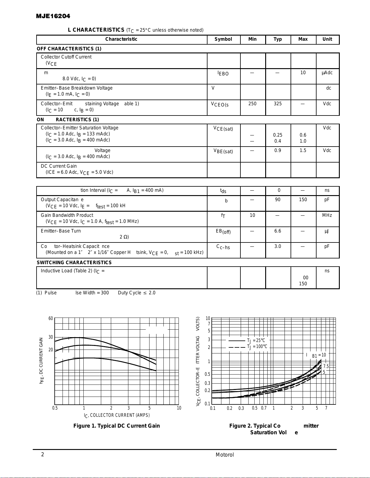
Figure 1. Typical DC Current Gain
IC, COLLECTOR CURRENT (AMPS)
0.5 2 10
20
h
FE
, DC CURRENT GAIN
1 53
30
7
0.7
TJ = 100°C
25°C
–55°C
7
10
5
3
50
VCE = 5 V
IC, COLLECTOR CURRENT (AMPS)
Figure 2. Typical Collector–Emitter
Saturation Voltage
0.5
3
0.2
5
10
1
0.1
7
0.3
2
0.7
0.5 32 50.7 1
0.1 0.2
TJ = 25°C
TJ = 100
°
C
IC/IB1 = 10
0.3
7
60
5
7.5
Page 3
3
Motorola Bipolar Power Transistor Device Data
0.2
C, CAPACITANCE (pF)
V
BE
, BASE–EMITTER VOLTAGE (VOLTS)
V
CE
, COLLECTOR–EMITTER VOLTAGE (VOLTS)
Figure 3. Typical Collector–Emitter
Saturation Region
IB, BASE CURRENT (AMPS)
0.7
0.1
0.03
0.3
0.3
6 A
0.05 1 2
2 A 3 AIC = 1 A
0.03
0.07 0.1 0.7
0.2 0.5
30
5
10
Figure 4. Typical Base–Emitter
Saturation Voltage
0.3 300.5
5
0.7
0.1
0.7 201 10
10
2
TJ = 25°C
2 3 5 7
IC, COLLECTOR CURRENT (AMPS)
TJ = 25°C
TJ = 100
°
C
0.3
Figure 5. Typical Capacitance
10K
VR, REVERSE VOLTAGE (VOLTS)
C
ib
0.1
1K
100
10
1 10 100 1K
2K
200
20
3K
300
5K
500
50
0.3 2 30 300
200.5 5 50 500
f
T
, TRANSITION FREQUENCY (MHz)
IC, COLLECTOR CURRENT (AMPS)
Figure 6. Typical Transition Frequency
VCE = 10 V
f
test
= 1 MHz
TC = 25°C
0 0.5 1 1.5 2 32.5
20
8
2
14
0
6
16
12
0.5
0.07
0.2
0.05
20
3
7
2
1
3
IC/IB1 = 5 to 10
7
1
3
0.5
30
0.2 3 200
TC = 25°C
10
4
18
C
ob
I
C
, COLLECTOR CURRENT (AMPS)
VCE, COLLECTOR–EMITTER VOLTAGE (VOLTS)
Figure 7. Maximum Forward Biased
Safe Operating Area
7
3
10
1
0.02
70
SECONDARY BREAKDOWN
WIREBOND LIMIT
THERMAL LIMIT
I
C
, COLLECTOR CURRENT (AMPS)
0.1
7 20 250
3
0.3
0.2
dc
TC = 25°C
1 ms
10 µs
2
5
0.5
50
7
0
150 550
IC/IB1 ≥ 5
TJ
≤
100°C
V
BE(off)
= 5 V
50
V
CE(pk)
, PEAK COLLECTOR–EMITTER VOLTAGE (VOLTS)
350
V
BE(off)
= 0 V
Figure 8. Maximum Reverse Biased
Safe Operating Area
3
5
2
1
250 450
0.03
0.07
0.05
0.01
0.7
1005 10 20030
MJE16204
6
4
SAFE OPERATING AREA
Page 4

4
Motorola Bipolar Power Transistor Device Data
SAFE OPERATING AREA INFORMATION
FORWARD BIAS
There are two limitations on the power handling ability of a
transistor: average junction temperature and second breakdown. Safe operating area curves indicate IC – VCE limits of
the transistor that must be observed for reliable operation;
i.e., the transistor must not be subjected to greater dissipation than the curves indicate.
The data of Figure 7 is based on TC = 25_C; T
J(pk)
is
variable depending on power level. Second breakdown pulse
limits are valid for duty cycles to 10% but must be derated
when TC ≥ 25_C. Second breakdown limitations do not derate the same as thermal limitations. Allowable current at the
voltages shown on Figure 7 may be found at any case temperature by using the appropriate curve on Figure 9.
At high case temperatures, thermal limitations will reduce
the power that can be handled to values less than the limitations imposed by second breakdown.
REVERSE BIAS
For inductive loads, high voltage and high current must be
sustained simultaneously during turn–off, in most cases, with
the base–to–emitter junction reverse biased. Under these
conditions the collector voltage must be held to a safe level
at or below a specific value of collector current. This can be
accomplished by several means such as active clamping,
RC snubbing, load line shaping, etc.
TC, CASE TEMPERATURE (°C)
0
40 120 160
0.6
POWER DERATING FACTOR
SECOND BREAKDOWN
DERATING
1
0.8
0.4
0.2
60 100 14080
THERMAL
DERATING
20
Figure 9. Power Derating
The safe level for these devices is specified as Reverse
Biased Safe Operating Area and represents the voltage–current condition allowable during reverse biased turnoff. This
rating is verified under clamped conditions so that the device
is never subjected to an avalanche mode. Figure 8 gives the
RBSOA characteristics.
H.P. 214
OR EQUIV.
P.G.
0
≈
–35 V
50
500
100
–V
2N5337
1
µ
F
+ –
+
–
0.02
µ
F
20
100
+V
≈
11 V
2N6191
A
R
B1
R
B2
10
µ
F
0.02
µ
F
T
1
+V
0 V
–V
A
50
*I
B
*I
C
T.U.T.
L
MR856
V
clamp
V
CC
I
C
V
CE
I
B
I
B1
I
B2
I
C(pk)
V
CE(pk)
T1[
L
coil(ICpk
)
V
CC
T1 adjusted to obtain I
C(pk)
V
(BR)CEO
L = 10 mH
RB2 = ∞
VCC = 20 Volts
RBSOA
L = 200 µH
RB2 = 0
VCC = 20 Volts
RB1 selected for desired I
B1
Note: Adjust –V to obtain desired V
BE(off)
at Point A.
*Tektronix
*P–6042 or
*Equivalent
Table 1. RBSOA/V
(BR)CEO(sus)
Test Circuit
Page 5

5
Motorola Bipolar Power Transistor Device Data
+24 V
C1
100
µ
F
+
U2
MC7812
V
I
V
O
G
N
D
C2
10
µ
F
+
Q2
MJ11016
(IB) R1
1 k
6.2 V
100 V
C3
10
µ
F
+
R7
2.7 k
R8
9.1 k
R9
470
R10
47
C5
0.1
C4
0.005
(DC)
R2
R510
R3
250
SYNC
Q1
BS170
R6
1 k
2
18
7 6
G
N
D
O
S
C
V
CC
% OUT
R10
470
1 W
Q3
MJE
15031
R12
470
1 W
D1
MUR110
T1
R4
22
LB
D2
MUR460
CY
V
CE
Q4
DUT
LY
C6
100
µ
F
R5
1 k
(IC)
Q5
MJ11016
+
T1: Ferroxcube Pot Core #1811 P3C8
Primary/Sec. Turns Ratio = 18:6
Primary Inductance Gap:
LP = 250 µH
LB = 0.5 µH
CY = 0.01 µF
LY = 13 µH
U1
MC1391P
Table 2. High Resolution Deflection Application Simulator
IC, COLLECTOR CURRENT (AMPS)
Figure 10. Typical Collector Current Storage
Time in Deflection Circuit Simulator
t
s
, STORAGE TIME (ns)
2K
700
200
300
ICI/B1 = 7.5
500
1K
1 2 753
10
IC, COLLECTOR CURRENT (AMPS)
Figure 11. Typical Collector Current Fall Time
in Deflection Circuit Simulator
t
f
, FALL TIME (ns)
100
20
50
200
2 3 5 71 10
30
70
TC = 25°C
ICI/B1 = 7.5
10
TC = 25°C
Page 6

6
Motorola Bipolar Power Transistor Device Data
Figure 12. Deflection Simulator Switching
Waveforms From Circuit in Table 2
I
C
0% I
B
V
CE
t
sv
VCE = 20 V
t
fi
10% I
C(pk)
Figure 13. Definition of Dynamic
Saturation Measurement
TIME (ns)
V
CE
DYNAMIC SATURATION TIME
IS MEASURED FROM VCE = 1 V
TO VCE = 5 V
t
ds
1
4
COLLECTOR–EMITTER VOLTAGE (VOLTS)
5
0
3
2
0
0
90% I
C(pk)
DYNAMIC DESATURATIION
The SCANSWITCH series of bipolar power transistors are
specifically designed to meet the unique requirements of horizontal deflection circuits in computer monitor applications.
Historically, deflection transistor design was focused on minimizing collector current fall time. While fall time is a valid
figure of merit, a more important indicator of circuit performance as scan rates are increased is a new characteristic,
“dynamic desaturation.” In order to assure a linear collector
current ramp, the output transistor must remain in hard saturation during storage time and exhibit a rapid turn–off transition. A sluggish transition results in serious consequences.
As the saturation voltage of the output transistor increases,
the voltage across the yoke drops. Roll off in the collector
current ramp results in improper beam deflection and distortion of the image at the right edge of the screen. Design
changes have been made in the structure of the SCANSWITCH series of devices which minimize the dynamic desaturation interval. Dynamic desaturation has been defined in
terms of the time required for the VCE to rise from 1.0 to
5.0 volts (Figures 12 and 13) and typical performance at optimized drive conditions has been specified. Optimization of
device structure results in a linear collector current ramp, excellent turn–off switching performance, and significantly lower overall power dissipation.
Page 7

7
Motorola Bipolar Power Transistor Device Data
t, TIME (ms)
0.01
0.01 0.05 1 2 5 10 20 50 5000.1 0.50.2
1
0.2
0.1
0.05
r(t), TRANSIENT THERMAL
R
θ
JC
(t) = r(t) R
θ
JC
R
θ
JC
= 1.56
°
C/W MAX
D CURVES APPLY FOR POWER
PULSE TRAIN SHOWN
READ TIME AT t
1
T
J(pk)
– TC = P
(pk)
R
θ
JC
(t)
P
(pk)
t
1
t
2
DUTY CYCLE, D = t1/t
2
SINGLE PULSE
RESISTANCE (NORMALIZED)
Figure 14. Typical Thermal Response for MJE16204
0.5
D = 0.5
0.7
0.07
0.02
0.02
100 200 10 k
0.2
0.05
0.1
0.02
0.01
Page 8

8
Motorola Bipolar Power Transistor Device Data
PACKAGE DIMENSIONS
CASE 221A–06
TO–220AB
ISSUE Y
NOTES:
1. DIMENSIONING AND TOLERANCING PER ANSI
Y14.5M, 1982.
2. CONTROLLING DIMENSION: INCH.
3. DIMENSION Z DEFINES A ZONE WHERE ALL
BODY AND LEAD IRREGULARITIES ARE
ALLOWED.
STYLE 1:
PIN 1. BASE
2. COLLECTOR
3. EMITTER
4. COLLECTOR
DIM MIN MAX MIN MAX
MILLIMETERSINCHES
A 0.570 0.620 14.48 15.75
B 0.380 0.405 9.66 10.28
C 0.160 0.190 4.07 4.82
D 0.025 0.035 0.64 0.88
F 0.142 0.147 3.61 3.73
G 0.095 0.105 2.42 2.66
H 0.110 0.155 2.80 3.93
J 0.018 0.025 0.46 0.64
K 0.500 0.562 12.70 14.27
L 0.045 0.060 1.15 1.52
N 0.190 0.210 4.83 5.33
Q 0.100 0.120 2.54 3.04
R 0.080 0.110 2.04 2.79
S 0.045 0.055 1.15 1.39
T 0.235 0.255 5.97 6.47
U 0.000 0.050 0.00 1.27
V 0.045 ––– 1.15 –––
Z ––– 0.080 ––– 2.04
B
Q
H
Z
L
V
G
N
A
K
F
1 2 3
4
D
SEATING
PLANE
–T–
C
S
T
U
R
J
How to reach us:
USA /EUROPE: Motorola Literature Distribution; JAPAN: Nippon Motorola Ltd.; Tatsumi–SPD–JLDC, Toshikatsu Otsuki,
P.O. Box 20912; Phoenix, Arizona 85036. 1–800–441–2447 6F Seibu–Butsuryu–Center, 3–14–2 Tatsumi Koto–Ku, Tokyo 135, Japan. 03–3521–8315
MFAX: RMFAX0@email.sps.mot.com – TOUCHTONE (602) 244–6609 HONG KONG: Motorola Semiconductors H.K. Ltd.; 8B Tai Ping Industrial Park,
INTERNET: http://Design–NET.com 51 Ting Kok Road, Tai Po, N.T., Hong Kong. 852–26629298
Motorola reserves the right to make changes without further notice to any products herein. Motorola makes no warranty , representation or guarantee regarding
the suitability of its products for any particular purpose, nor does Motorola assume any liability arising out of the application or use of any product or circuit,
and specifically disclaims any and all liability, including without limitation consequential or incidental damages. “T ypical” parameters can and do vary in different
applications. All operating parameters, including “T ypicals” must be validated for each customer application by customer’s technical experts. Motorola does
not convey any license under its patent rights nor the rights of others. Motorola products are not designed, intended, or authorized for use as components in
systems intended for surgical implant into the body, or other applications intended to support or sustain life, or for any other application in which the failure of
the Motorola product could create a situation where personal injury or death may occur. Should Buyer purchase or use Motorola products for any such
unintended or unauthorized application, Buyer shall indemnify and hold Motorola and its officers, employees, subsidiaries, affiliates, and distributors harmless
against all claims, costs, damages, and expenses, and reasonable attorney fees arising out of, directly or indirectly, any claim of personal injury or death
associated with such unintended or unauthorized use, even if such claim alleges that Motorola was negligent regarding the design or manufacture of the part.
Motorola and are registered trademarks of Motorola, Inc. Motorola, Inc. is an Equal Opportunity/Affirmative Action Employer.
MJE16204/D
*MJE16204/D*
◊
 Loading...