

Page 1
HIGH VOLTAGE FAST-SWITCHING
■ STMicroelectronicsPREFERRED
SALESTYPE
■ HIGHVOLTAGECAPABILITY
■ SURFACE-MOUNTING TO-252(DPAK)
POWERPACKAGE INTAPE &REEL
(SUFFIX”T4”)
■ ELECTRICALLY SIMILAR TO TIP50
APPLICATIONS
■ SWITCHMODEPOWERSUPPLIES
■ AUDIO AMPLIFIERS
■ GENERALPURPOSE SWITCHINGAND
AMPLIFIER
DESCRIPTION
The MJD50 is manufactured using Medium
VoltageEpitaxial Planar technology,resulting in a
rugged high performancecost-effectivetransistor.
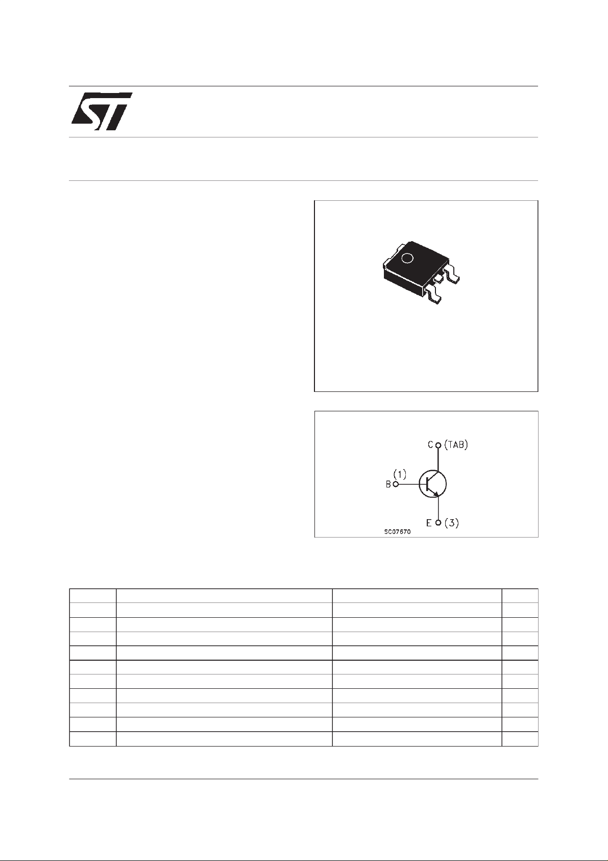
MJD50
NPN POWER TRANSISTOR
3
1
DPAK
TO-252
(Suffix”T4”)
INTERNAL SCHEMATIC DIAGRAM
ABSOLUTE MAXIMUM RATINGS
Symb o l Parame t er Val u e Uni t
V
V
V
I
I
P
T
January 2000
Collector-Base Voltage (IE= 0) 500 V
CBO
Collect or- E m itter Volta ge (IB= 0) 400 V
CEO
Emitter-Base Voltage ( IC=0) 5 V
EBO
Collect or Current 1 A
I
C
Collect or Peak Current (tp<5ms) 2 A
CM
I
Base Current 0.6 A
B
Base Peak Cur rent (tp<5ms) 1.2 A
BM
Total Dissipation at Tc=25oC15W
tot
Stora ge T emperat u re -65 to 150
stg
Max. Op erat ing J unction Temperature 150
T
j
o
C
o
C
1/6
Page 2
MJD50
THERMAL DATA
R
thj-case
R
thj- amb
Ther mal Resi stance Junct ion-case Max
Ther mal Resi stance J unct i on- ambient Max
8.33
100
o
C/W
o
C/W
ELECTRICAL CHARACTERISTICS (T
=25oC unlessotherwisespecified)
case
Symbol Parameter Test Conditions Min. Typ. Max. Unit
I
CES
I
CEO
I
EBO
V
CEO(sus )
Collec t or Cut -of f
Current (V
BE
=0)
Collec t or Cut -of f
Current (I
B
=0)
Emit ter Cut-of f C urr ent
(I
=0)
C
∗ Collec t or- E m itter
V
=500V 0.1 mA
CE
V
=300V 0.1 mA
CE
=5V 1 mA
V
EB
I
= 30 mA 400 V
C
Sust aining Volta ge
=0)
(I
B
V
CE(sat)
∗ Collec t or -Emitter
IC=1A IB=0.2A 1 V
Sat uration Vol t age
∗ Base-Emitt er O n
V
BE(on)
IC=1A VCE=10V 1.5 V
Voltage
∗ DC Current Gain IC=0.3A VCE=10V
h
FE
f
h
Tr ansition Frequenc y IC=0.2A VCE= 10 V f= 2MHz 10 M Hz
T
Small Signal Curr ent
fe
=1A VCE=10V
I
C
IC=0.2A VCE= 10 V f= 1kHz 25
30
10
150
Gain
∗
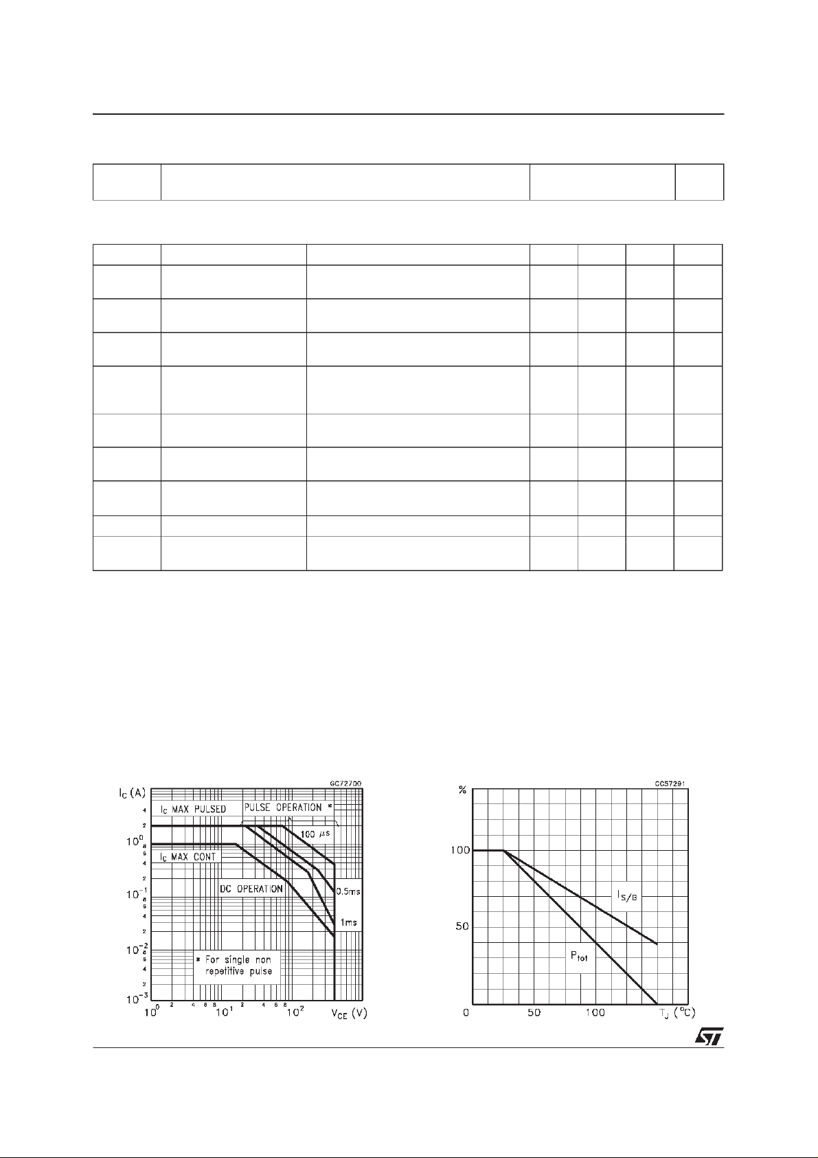
Pulsed: Pulse duration = 300 µs, duty cycle 1.5 %
SafeOperatingArea Derating Curves
2/6
Page 3

MJD50
DCCurrent Gain
Collector-Emitter SaturationVoltage
DC Current Gain
Collector-EmitterSaturationVoltage
Base-EmitterSaturationVoltage
Collector-BaseCapacitance
3/6
Page 4

MJD50
SwitchingTimeInductiveLoad SwitchingTime InductiveLoad
SwitchingTimeInductiveLoad SwitchingTime InductiveLoad
4/6
Page 5

TO-252 (DPAK) MECHANICAL DATA
MJD50
DIM.
mm inch
MIN. TYP. MAX. MIN. TYP. MAX.
A 2.20 2.40 0.087 0.094
A1 0.90 1.10 0.035 0.043
A2 0.03 0.23 0.001 0.009
B 0.64 0.90 0.025 0.035
B2 5.20 5.40 0.204 0.213
C 0.45 0.60 0.018 0.024
C2 0.48 0.60 0.019 0.024
D 6.00 6.20 0.236 0.244
E 6.40 6.60 0.252 0.260
G 4.40 4.60 0.173 0.181
H 9.35 10.10 0.368 0.398
L2 0.8 0.031
L4 0.60 1.00 0.024 0.039
V2 0
o
o
8
o
0
o
0
P032P_B
5/6
Page 6

MJD50
Information furnished is believed to beaccurate and reliable. However, STMicroelectronics assumes noresponsibility for the consequences
of use of such information nor for any infringement of patents or other rights of third parties which may result from its use. No license is
granted by implication or otherwise under any patent or patent rights of STMicroelectronics. Specification mentioned in this publication are
subject to change without notice. This publication supersedes and replaces all information previously supplied. STMicroelectronics products
are not authorized for use as critical components in life support devices or systems without express written approval of STMicroelectronics.
The ST logo is a trademark of STMicroelectronics
2000 STMicroelectronics – Printed in Italy – All Rights Reserved
STMicroelectronicsGROUP OF COMPANIES
Australia - Brazil - China - Finland - France - Germany - Hong Kong - India - Italy - Japan - Malaysia - Malta - Morocco -
Singapore-Spain - Sweden - Switzerland -United Kingdom - U.S.A.
http://www.st.com
6/6
 Loading...