

Page 1
MJD31B/31C
MJD32B/32C
COMPLEMENTARY SILICON POWER TRANSISTORS
■ STMicroelectronicsPREFERRED
SALESTYPES
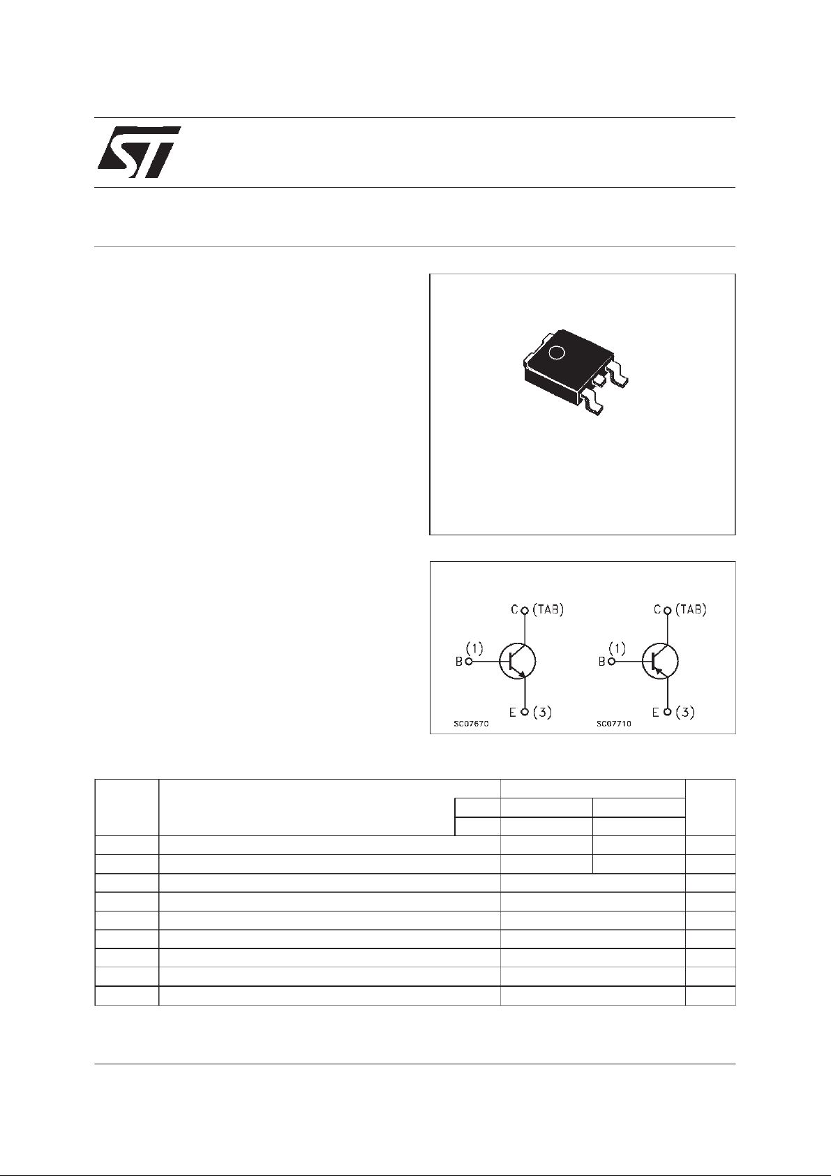
■ SURFACE-MOUNTING TO-252 (DPAK)
POWERPACKAGEIN TAPE & REEL
(SUFFIX”T4”)
■ ELECTRICALLY SIMILAR TO TIP31B/CAND
TIP32B/C
APPLICATIONS
■ GENERALPURPOSE SWITCHING AND
AMPLIFIERTRANSISTORS
DESCRIPTION
The MJD31B and MJD31C and the MJD32B and
MJD32C form complementary NPN-PNP pairs.
They are manufactured using Epitaxial Base
technologyfor cost-effectiveperformance.
DPAK
TO-252
(Suffix ”T4”)
3
1
INTERNAL SCHEMATIC DIAGRAM
ABSOLUTE MAXIMUM RATINGS
Symbol Parameter Value Unit
NPN MJD31B MJD31C
PNP MJD32B MJD32C
V
V
V
I
P
T
For PNP types the values are intentednegative.
Collector-Base Voltage (IE=0) 80 100 V
CBO
Collector-Emitter Voltage (IB=0) 80 100 V
CEO
Emitter-Base Voltage (IC=0) 5 V
EBO
Collector Cur rent 3 A
I
C
Collector Pe ak C urrent 5 A
CM
Base Current 1 A
I
B
Tot al D iss ip at i on at Tc=25oC15W
tot
Sto rage Temperature -65 t o 1 50
stg
Max. O perating J unction Temperat u r e 150
T
j
o
C
o
C
May 1999
1/5
Page 2
MJD31B/31C- MJD32B/32C
THERMAL DATA
R
thj-case
R
thj-amb
Ther mal Res ist ance Junction-case Max
Ther mal Res ist ance Junction-ambie nt Max
8.33
100
o
C/W
o
C/W
ELECTRICAL CHARACTERISTICS (T
=25oC unlessotherwisespecified)
case
Symbol Parameter Test C ondition s Min. Typ. Max. Unit
I
CES
I
CEO
I
EBO
V
CEO(sus)
V
CE(sat)
Collec t or Cut- off
Current (V
BE
=0)
Collec t or Cut- off
Current (I
B
=0)
Emitt er Cut -of f Current
(I
=0)
C
Collec t or -Emit ter
Sust aining Voltage
∗ Collec t or -Emit ter
V
= Ma x Rat i ng 20 µA
CE
V
=60V 50 µA
CE
=5V 0.1 mA
V
EB
IC=30mA
for MJ D31B / 32B
for MJ D31C / 32C
80
100
IC=3A IB= 3 75 m A 1.2 V
Saturation Voltage
∗ Base-Emi tter Voltag e IC=3A VCE=4V 1.8 V
V
BE(on)
h
∗ DC Current Gain IC=1A VCE=4V
FE
h
∗
Pulsed: Pulse duration = 300 µs, duty cycle ≤ 2%
For PNP typevoltage and current values are negative.
Dynamic Curr e nt Gain IC=0.5A VCE=10V f=1KHz
fe
=3A VCE=4V
I
C
=0.5A VCE=10V f=1MHz203
I
C
25
10 50
V
V
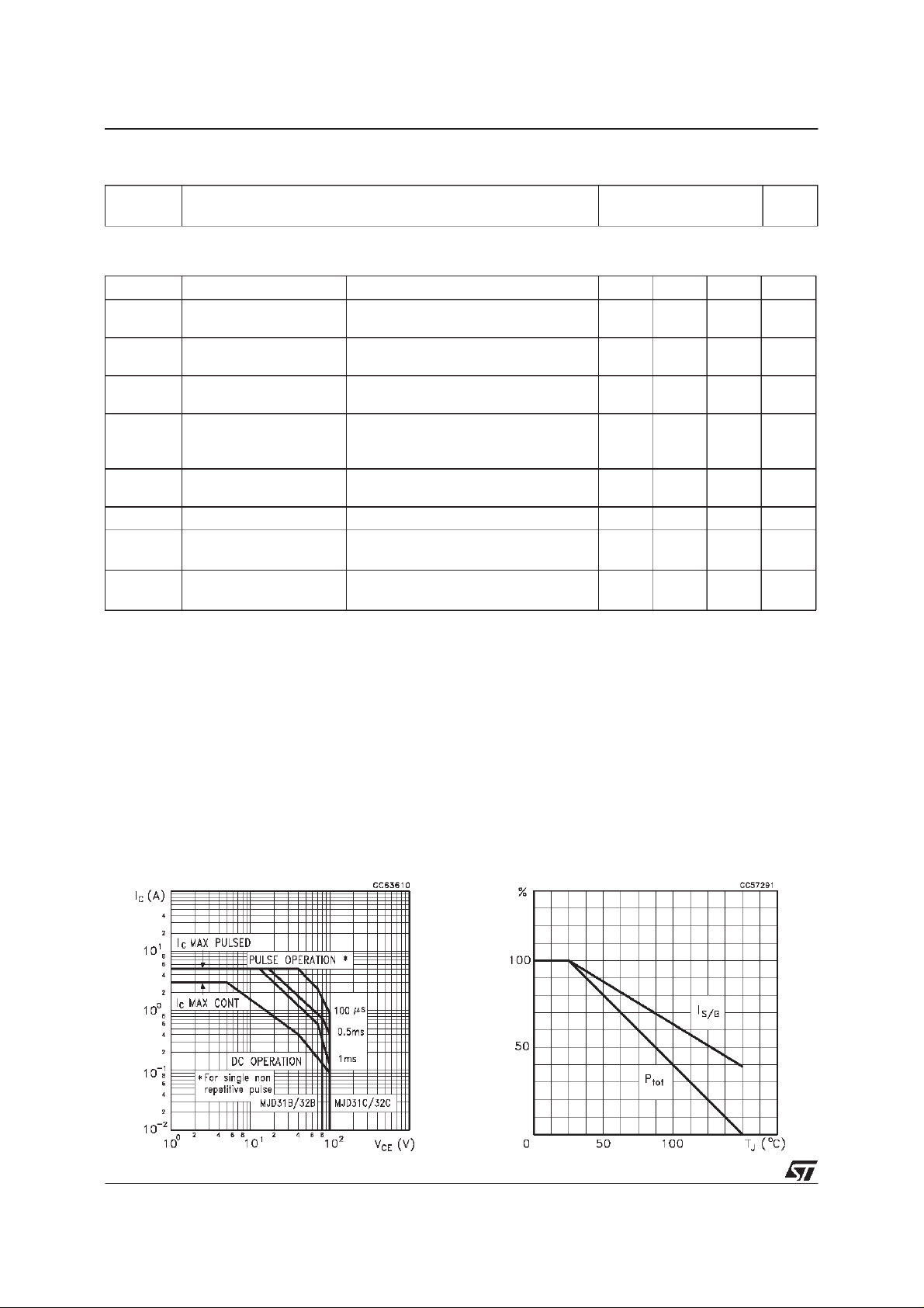
Safe Operating Area DeratingCurves
2/5
Page 3

MJD31B/31C - MJD32B/32C
DCCurrent Gain (NPNtype)
Collector-EmitterSaturationVoltage (NPN type)
DC Current Gain (PNPtype)
Collector-EmitterSaturationVoltage (PNPtype)
Base-EmitterSaturation Voltage (NPN type)
Collector-BaseCapacitance (PNP type)
3/5
Page 4

MJD31B/31C- MJD32B/32C
TO-252 (DPAK) MECHANICAL DATA
DIM.
mm inch
MIN. TYP. MAX. MIN. TYP. MAX.
A 2.20 2.40 0.087 0.094
A1 0.90 1.10 0.035 0.043
A2 0.03 0.23 0.001 0.009
B 0.64 0.90 0.025 0.035
B2 5.20 5.40 0.204 0.213
C 0.45 0.60 0.018 0.024
C2 0.48 0.60 0.019 0.024
D 6.00 6.20 0.236 0.244
E 6.40 6.60 0.252 0.260
G 4.40 4.60 0.173 0.181
H 9.35 10.10 0.368 0.398
L2 0.8 0.031
L4 0.60 1.00 0.024 0.039
V2 0
o
o
8
o
0
o
0
4/5
P032P_B
Page 5

MJD31B/31C - MJD32B/32C
Information furnished is believed tobe accurate and reliable. However, STMicroelectronics assumes no responsibility for the consequences
of use of such information nor for any infringement of patents or other rights of third parties which may result from its use. No license is
granted by implication or otherwise under any patent or patent rights of STMicroelectronics. Specification mentioned in this publication are
subject to change without notice.This publication supersedes and replaces all information previously supplied. STMicroelectronics products
are not authorized for use as critical components in life support devices or systems without express written approval of STMicroelectronics.
The ST logo is a trademark of STMicroelectronics
1999 STMicroelectronics – Printed in Italy – All Rights Reserved
STMicroelectronicsGROUP OF COMPANIES
Australia - Brazil - Canada - China -France - Germany - Italy - Japan - Korea - Malaysia - Malta - Mexico - Morocco - The Netherlands -
Singapore - Spain -Sweden - Switzerland - Taiwan - Thailand - United Kingdom - U.S.A.
http://www.st.com
.
5/5
 Loading...