

Page 1
MJD122-1 / MJD122T4
MJD127-1 / MJD127T4
COMPLEMENTARY POWER
DARLINGTON TRANSISTORS
Ordering
Code
MJD122T4
MJD122-1
MJD127T4
MJD127-1
■ STMicroelectronics PREFERREDSALESTYPES
■ LOW BASE-DRIVE REQUIREMENTS
■ INTEGRATED ANTIPARALLEL
Marking Package Shipment
MJD122
MJD122
MJD127
MJD127
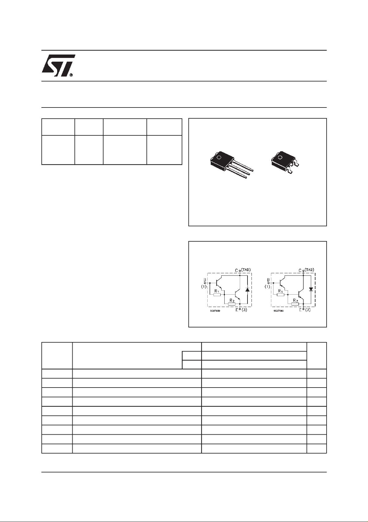
TO-252 (DPAK)
TO-251 (IPAK)
TO-252 (DPAK)
TO-251 (IPAK)
Tape& Reel
Tube
Tape& Reel
Tube
COLLECTOR-EMITTER DIODE
■ THROUGH HOLE TO-251 (IPAK)
POWER PACKAGE IN TUBE (SUFFIX “-1”)
■ SURFACE MOUNTING TO-252 (DPAK)
POWER PACKAGE IN TAPE & REEL
(SUFFIX “T4”)
■ ELECTRICALLY SIMILAR TO TIP122 AND
TIP127
APPLICATIONS:
■ GENERAL PURPOSE SWITCHINGAND
AMPLIFIER
DESCRIPTION
The MJD122 and MJD127 form complementary
NPN - PNP pair. They are manufactured using
Epit axia l B ase tec hnology f or c os t-ef f ect ive
performance.
3
1
TO-251
IPAK
(Suffix ”-1”)
3
2
1
TO-252
DPAK
(Suffix ”T4”)
INTERNAL SCHEMATIC DIAGRAM
Typ. = 150 Ω
R1Typ. = 10 KΩ
R
2
ABSOLUTE MAXIMUM RATINGS
Symbol Parameter Value Unit
NPN MJD122
PNP MJD127
V
CBO
V
CEO
V
EBO
I
I
CM
I
P
T
stg
T
For PNP types voltage and current values are negative.
Collector-Base Voltage (IE=0)
Collector-Emitter Voltage (IB=0)
Emitter-Base Voltage (IC=0)
Collector Current 5 A
C
Collector Peak Current (tp< 5 ms)
Base Current 0.1 A
B
TotalDissipation at Tc=25°C
tot
Storage Temperature –65 to 150 °C
Max. Operating Junction Temperature 150 °C
j
100 V
100 V
5V
8A
20 W
1/8August 2002
Page 2
MJD122-1 / MJD122T4 / MJD127-1 / MJD127T4
THERMAL DATA
R
thj-case
R
thj-amb
ELECTRICAL CHARACTERISTICS (Tj=25°C unless otherwise specified)
Symbol Parameter Test Conditions Min. Typ. Max. Unit
I
CBO
I
CEO
I
CEX
I
EBO
V
CEO(sus)
V
CE(sat)
V
BE(sat)
V
BE(on)
h
FE
* Pulsed: Pulse duration = 300 µs, duty cycle ≤ 2%.
For PNP types voltage and current values are negative.
Thermal Resistance Junction-case
Thermal Resistance Junction-ambient
Collector Cut-off
Current (I
E
=0)
Collector Cut-off
Current (I
B
=0)
Collector Cut-off
Current (V
= -1.5 V)
BE
Emitter Cut-off Current
(I
=0)
C
* Collector-Emitter
= 100 V 10 µA
V
CB
=50V 10 µA
V
CE
= 100 V
V
CE
= 100 V
V
CE
=5V 2 mA
V
EB
= 30 mA 100 V
I
C
Sustaining Voltage
(I
=0)
B
* Collector-Emitter
Saturation Voltage
* Base-Emitter
IC=4A
=8A
I
C
IC=8A IB= 80 mA 4.5 V
Saturation Voltage
* Base-Emitter On
IC=4A VCE= 4 V 2.8 V
Voltage
* DC Current Gain IC=4A
=8A
I
C
T
=125°C
j
I
=16mA
B
=80mA
I
B
V
=4V
CE
=4V
V
CE
Max
Max
1000
100
6.25
100
10
500µAµA
2
4
12000
°C/W
°C/W
V
V
2/8
Page 3
MJD122-1 / MJD122T4 / MJD127-1 / MJD127T4
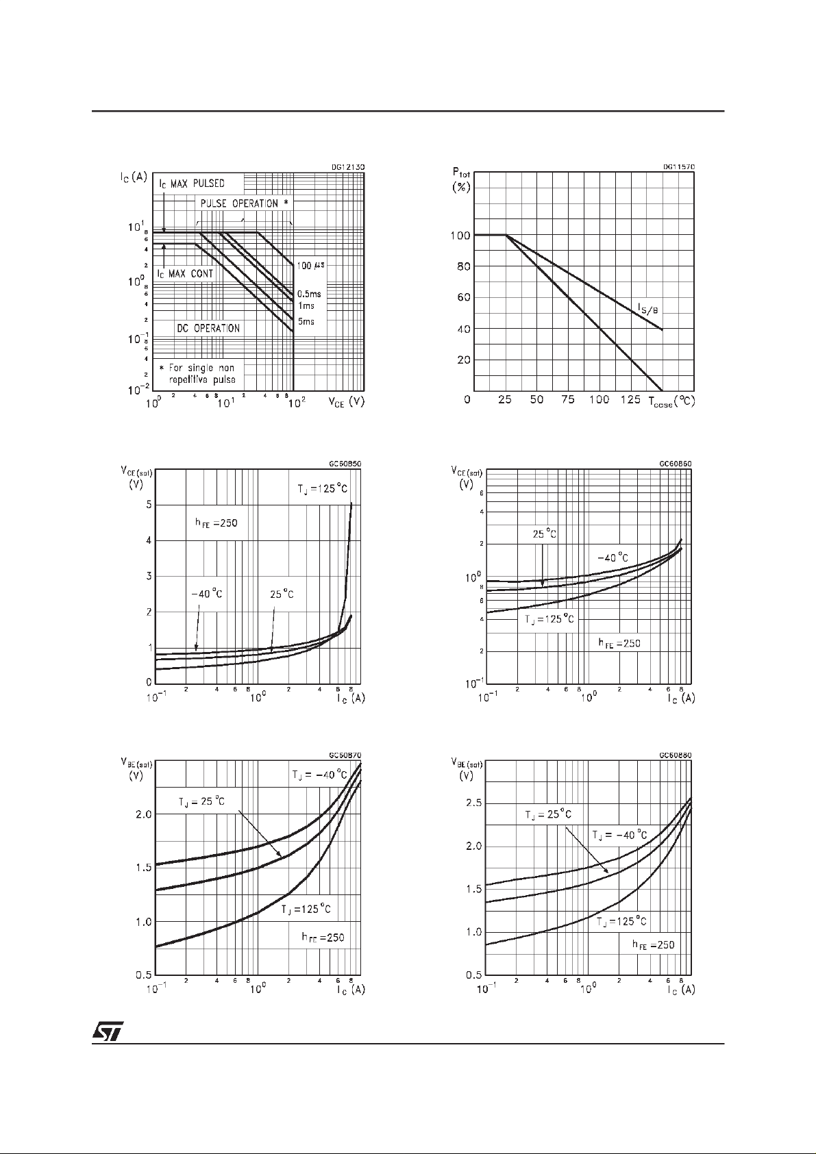
Safe Operating Area Derating Curve
Collector-Emitter Saturation Voltage (PNP type)Collector-Emitter Saturation Voltage (NPN type)
Base-Emitter Saturation Voltage (NPN type)
Base-Emitter Saturation Voltage (PNP type)
3/8
Page 4

MJD122-1 / MJD122T4 / MJD127-1 / MJD127T4
Base-Emitter On Voltage (NPN type)
DC Current Gain (NPN type)
Base-Emitter On Voltage (PNP type)
DC Current Gain (PNP type)
Switching Times Resistive Load (NPN type) Switching Times Resistive Load (PNP type)
4/8
Page 5

MJD122-1 / MJD122T4 / MJD127-1 / MJD127T4
Freewheel Diode Forward Voltage (NPN type) Freewheel Diode Forward Voltage (PNP type)
5/8
Page 6

MJD122-1 / MJD122T4 / MJD127-1 / MJD127T4
TO-251 (IPAK) MECHANICAL DATA
DIM.
A 2.20 2.40 0.087 0.094
A1 0.90 1.10 0.035 0.043
A3 0.70 1.30 0.028 0.051
B 0.64 0.90 0.025 0.035
B2 5.20 5.40 0.204 0.213
B3 0.85 0.033
B5 0.30 0.012
B6 0.95 0.037
C 0.45 0.60 0.018 0.024
C2 0.48 0.60 0.019 0.024
D 6.00 6.20 0.237 0.244
E 6.40 6.60 0.252 0.260
G 4.40 4.60 0.173 0.181
H 15.90 16.30 0.626 0.642
L 9.00 9.40 0.354 0.370
L1 0.80 1.20 0.031 0.047
L2 0.80 1.00 0.031 0.039
V1 10
MIN. TYP. MAX. MIN. TYP. MAX.
mm inch
o
10
o
6/8
P032N_E
Page 7

MJD122-1 / MJD122T4 / MJD127-1 / MJD127T4
TO-252 (DPAK) MECHANICAL DATA
DIM.
mm inch
MIN. TYP. MAX. MIN. TYP. MAX.
A 2.20 2.40 0.087 0.094
A1 0.90 1.10 0.035 0.043
A2 0.03 0.23 0.001 0.009
B 0.64 0.90 0.025 0.035
B2 5.20 5.40 0.204 0.213
C 0.45 0.60 0.018 0.024
C2 0.48 0.60 0.019 0.024
D 6.00 6.20 0.236 0.244
E 6.40 6.60 0.252 0.260
G 4.40 4.60 0.173 0.181
H 9.35 10.10 0.368 0.398
L2 0.8 0.031
L4 0.60 1.00 0.024 0.039
V2 0
o
o
8
o
0
o
0
P032P_B
7/8
Page 8

MJD122-1 / MJD122T4 / MJD127-1 / MJD127T4
Information furnished is believed to be accurate and reliable. However, STMicroelectronics assumes no responsibility for the
consequences of use ofsuch information nor for anyinfringement of patents orother rights ofthird parties which mayresult from
its use. No license is granted by implication or otherwise under any patent or patent rights of STMicroelectronics. Specifications
mentioned in this publication are subject to change without notice. This publication supersedes and replaces all information
previously supplied. STMicroelectronics products are not authorized for use as critical components in life support devices or
systems without express written approval of STMicroelectronics.
Australia - Brazil - Canada - China - Finland - France - Germany - Hong Kong - India - Israel - Italy - Japan - Malaysia - Malta - Morocco
The ST logo is a registered trademark of STMicroelectronics
2002 STMicroelectronics - Printed in Italy - All Rights Reserved
Singapore - Spain - Sweden - Switzerland - United Kingdom - United States.
STMicroelectronics GROUP OF COMPANIES
http://www.st.com
8/8
 Loading...