

Page 1
COMPLEMENTARY SILICON POWER
■ SGS-THOMSONPREFERREDSALESTYPES
■ LOW BASE-DRIVE REQUIREMENTS
■ INTEGRATEDANTIPARALLEL
COLLECTOR-EMITTER DIODE
■ SURFACE-MOUNTING TO-252 (DPAK)
POWER PACKAGE IN TAPE & REEL
(SUFFIX ”T4”)
■ ELECTRICALSIMILAR TO TIP112 AND
TIP117
APPLICATIONS
■ GENERALPURPOSE SWITCHING AND
AMPLIFIER
DESCRIPTION
The MJD112 and MJD117 form complementary
PNP - NPN pairs.
They are manufactured using Epitaxial Base
technologyfor cost-effective performance.
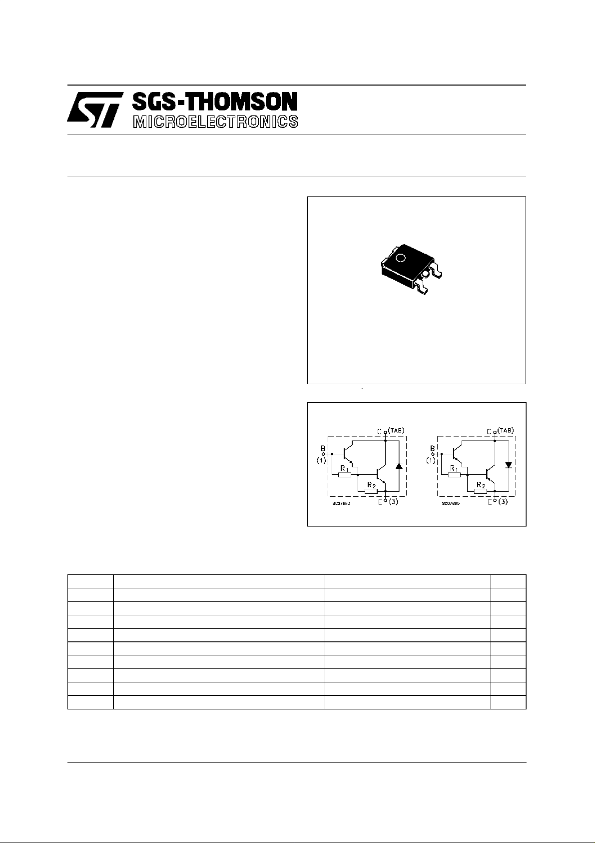
MJD112
MJD117
DARLINGTONTRANSISTORS
3
1
DPAK
TO-252
(Suffix ”T4”)
INTERNAL SCHEMATIC DIAGRAM
R1(typ)= 7KΩ
R2(typ)= 200Ω
ABSOLUTE MAXIMUM RATINGS
Symbol Parameter Value Unit
V
V
V
I
P
T
ForPNP type voltageand currentvalues are negative.
September1997
Collector-Emitter Voltage (IE= 0) 100 V
CBO
Collector-Emitter Voltage (IB= 0) 100 V
CEO
Emitter-Base Voltage (IC=0) 5 V
EBO
Collector Current 2 A
I
C
Collector Peak Current (tp<5ms) 4 A
CM
Base Current 0.05 A
I
B
Tota l Dissipa tio n at Tc=25oC20W
tot
Storage Temperature -65 to 150
stg
Max. OperatingJu nctionTemperature 150
T
j
o
C
o
C
1/6
Page 2
MJD112/MJD117
THERMAL DATA
R
thj-case
R
thj-amb
Thermal Resistance Junction-case Max
Thermal Resistance Junction-ambient Max
6.25
100
o
C/W
o
C/W
ELECTRICAL CHARACTERISTICS (T
=25oC unless otherwise specified)
case
Symbol Parameter Test Conditions Min. Typ. Max. Unit
I
CBO
I
CEO
I
CEX
I
EBO
V
CEO(sus)
Collector Cut-off
Curren t (I
E
=0)
Collector Cut-off
Curren t (I
B
=0)
Collector Cut-off
Current
Emitter Cut-off Current
(I
=0)
C
Collector-Emitter
= 100 V
V
CB
V
=80V
CB
= 50 V 0.02 mA
V
CE
VCB=80V VBE= -1.5V
V
=80V VBE= -1.5V Tc= 125oC
CB
=5V 2 mA
V
EB
0.02
0.01mAmA
0.01
0.5
IC= 30 mA 100 V
Sustaining Voltage
V
CE(sat)
V
BE(sat)
∗ Collector-Emitter
Saturation Voltage
∗ Collector-Base
IC=2A IB=8mA
I
=4A IB=40mA
C
2
3
IC=4A IB=40mA 4 V
Saturation Voltage
∗ Base-Emit ter V o ltage IC=2A VCE=3V 2.8 V
V
BE(on)
h
∗ DC Current Gain IC=0.5A VCE=3V
FE
∗ Pulsed:Pulseduration = 300 µs, duty cycle ≤ 2%
I
=2A VCE=3V
C
I
=4A VCE=3V
C
500
1000
200
12000
mA
mA
V
V
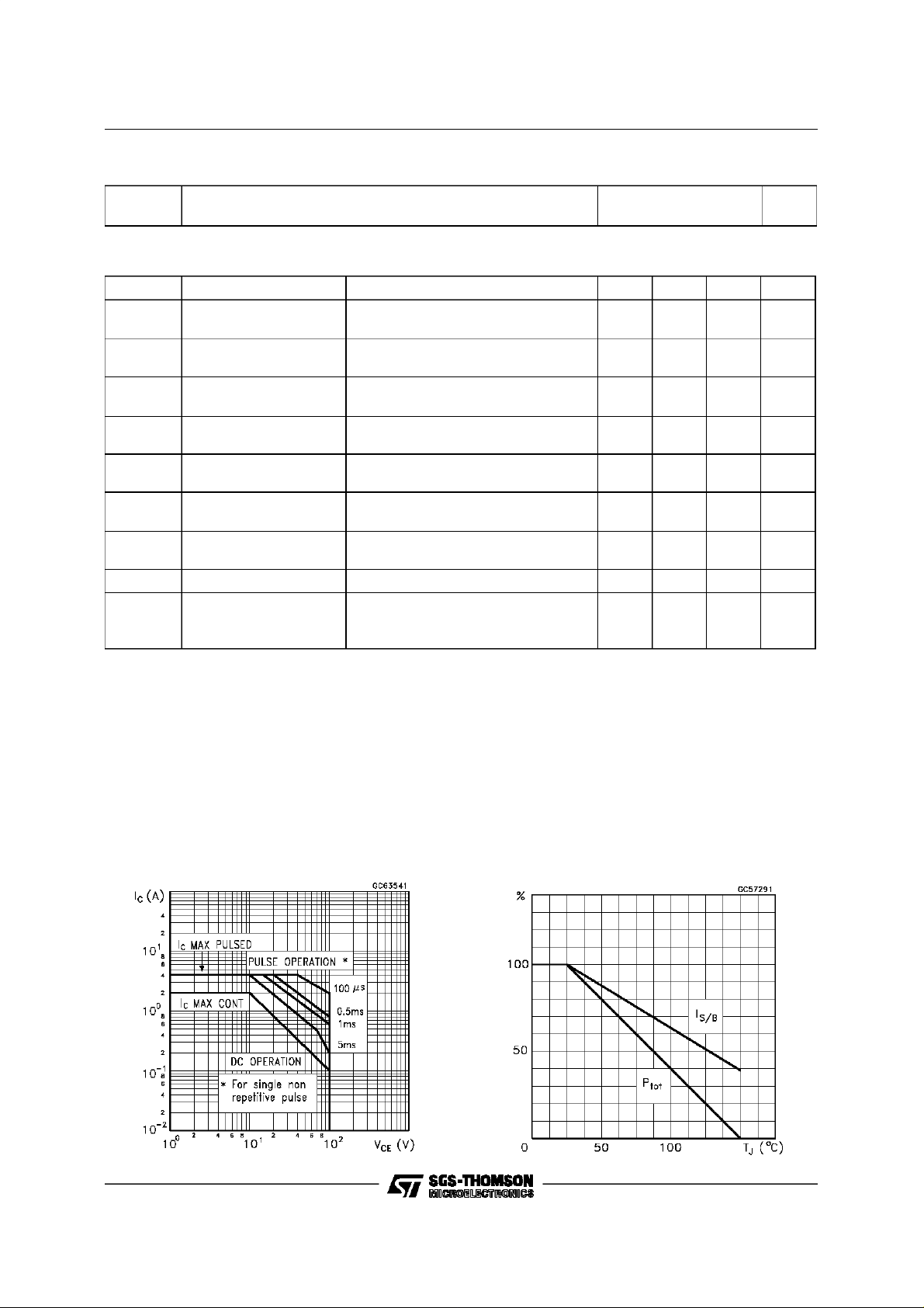
Safe OperatingAreas Derating Curve
2/6
Page 3
MJD112/MJD117
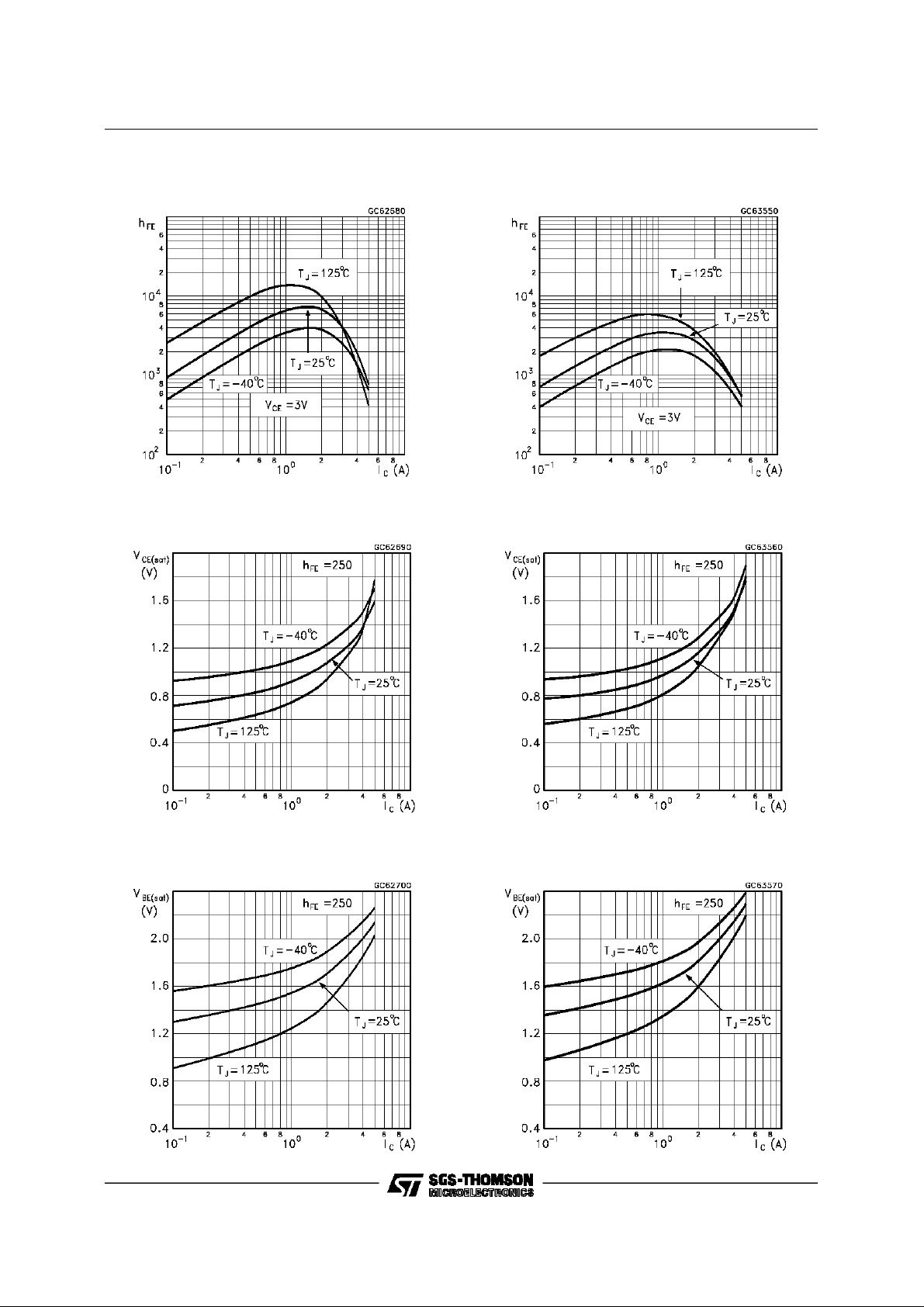
DC Current Gain (NPN type)
Collector-Emitter Saturation Voltage (NPN type)
DC Current Gain (NPN type)
Collector-Emitter Saturation Voltage (PNP type)
Base-EmitterSaturation Voltage (NPN type)
Base-Emitter Saturation Voltage (PNP type)
3/6
Page 4

MJD112/MJD117
Base-EmitterOn Voltage (NPN type) Base-Emitter On Voltage(PNP type)
Freewheel Diode Forward Voltage (NPN types) FreewheelDiode Forward Voltage (PNP types)
4/6
Page 5

TO-252 (DPAK) MECHANICAL DATA
MJD112/MJD117
DIM.
mm inch
MIN. TYP. MAX. MIN. TYP. MAX.
A 2.2 2.4 0.086 0.094
A1 0.9 1.1 0.035 0.043
A2 0.03 0.23 0.001 0.009
B 0.64 0.9 0.025 0.035
B2 5.2 5.4 0.204 0.212
C 0.45 0.6 0.017 0.023
C2 0.48 0.6 0.019 0.023
D 6 6.2 0.236 0.244
E 6.4 6.6 0.252 0.260
G 4.4 4.6 0.173 0.181
H 9.35 10.1 0.368 0.397
L2 0.8 0.031
L4 0.6 1 0.023 0.039
H
A
E
C2
L2
B2
==
==
DETAIL”A”
D
2
13
L4
A1
C
A2
DETAIL”A”
B
G
==
0068772-B
5/6
Page 6

MJD112/MJD117
Informationfurnished is believed to be accurate and reliable. However, SGS-THOMSON Microelectronicsassumes no responsability for the
consequencesof use of such information nor for any infringementof patents or otherrightsof thirdparties whichmay results from its use. No
license is grantedby implicationor otherwiseunder any patentor patentrights of SGS-THOMSON Microelectronics.Specifications mentioned
in thispublication are subjectto change withoutnotice. This publicationsupersedesand replacesall informationpreviously supplied.
SGS-THOMSON Microelectronicsproductsarenotauthorizedforuseas critical componentsin lifesupportdevices or systemswithoutexpress
written approvalof SGS-THOMSONMicroelectonics.
1997 SGS-THOMSONMicroelectronics - Printed in Italy - All RightsReserved
Australia- Brazil - Canada - China- France - Germany- Hong Kong - Italy- Japan- Korea - Malaysia - Malta - Morocco - TheNetherlands -
Singapore - Spain- Sweden - Switzerland - Taiwan - Thailand - UnitedKingdom- U.S.A
SGS-THOMSONMicroelectronicsGROUP OF COMPANIES
...
6/6
 Loading...