

Page 1
®
PNP SILICON POWER TRANSISTOR
■ SURFACE-MOUNT ING D
POWER PACKAGE IN TAPE & REEL
(SUFFIX "T4")
■ ELECTRICALLY SIMILAR TO TIP32B
APPLICATION
■ LINEAR AND SWITCHING INDUSTRIAL
EQUIPMENT
DESCRIPTION
The MJB32B is manufactured using
Epitaxial-base Technology for use in medium
power linear and switching applications.
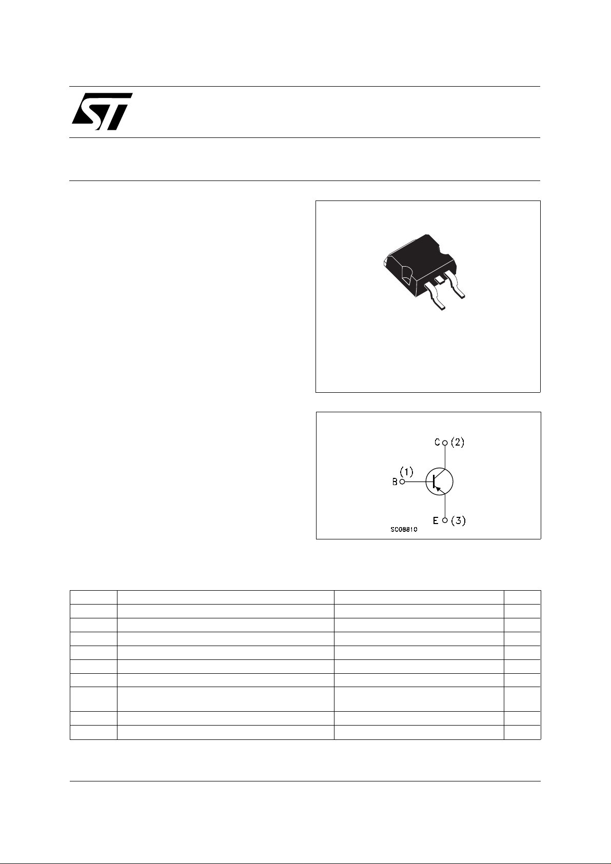
2
PAK (TO-263)
MJB32B
3
1
D2PAK
(TO-263)
(Suffix "T4")
INTER NAL SCH E M ATI C DIAG RA M
ABSOLUTE MAXIMUM RATINGS
Symbol Parameter Value Unit
V
V
V
I
P
T
Collector-Base Voltage (IE = 0) -80 V
CBO
Collector-Emitter Voltage (IB = 0) -80 V
CEO
Emitter-Base Voltage (IC = 0) -5 V
EBO
Collector Current -3 A
I
C
Collector Peak Current -5 A
CM
Base Current -1 A
I
B
Total Dissipation at T
tot
T
Storage Temperature -65 to 150
stg
T
Max. Operating Junction Temperature 150
j
case
amb
≤ 25 oC
≤ 25 oC
40
2
W
W
o
C
o
C
June 2001
1/5
Page 2
MJB32B
THERMAL DATA
R
thj-case
R
thj-amb
Thermal Resistance Junction-case Max
Thermal Resistance Junction-ambient Max
3.12
62.5
o
C/W
o
C/W
ELECTRICAL CHARACTERISTICS (T
= 25 oC unless otherwise specified)
case
Symbol Parameter Test Conditions Min. Typ. Max. Unit
I
CEO
I
CES
I
EBO
V
CEO(sus)
Collector Cut-off
Current (I
= 0)
B
Collector Cut-off
Current (V
BE
= 0)
Emitter Cut-off Current
(I
= 0)
C
∗ Collector-Emitter
= -60 V -50 µA
V
CE
= -80 V -20 µA
V
CE
= -5 V -0.1 mA
V
EB
I
= -30 mA -80 V
C
Sustaining Voltage
(I
= 0)
B
∗ Collector-Emitter
V
CE(sat)
IC = -3 A IB = -375 mA -1.2 V
Saturation Voltage
V
∗ Base-Emitter Voltage IC = -3 A VCE = -4 V -1.8 V
BE
hFE∗ DC Current Gain IC = -1 A VCE = -4 V
I
= -3 A VCE = -4 V
C
h
∗ Pulsed : pulse duration = 300 µs, duty cycle ≤ 2%
Small Signall Current
fe
Gain
IC = -0.5 A VCE = -10 V f = 1 KHz
I
= -0.5 A VCE = -10 V f = 1 MHz
C
25
10 50
20
3
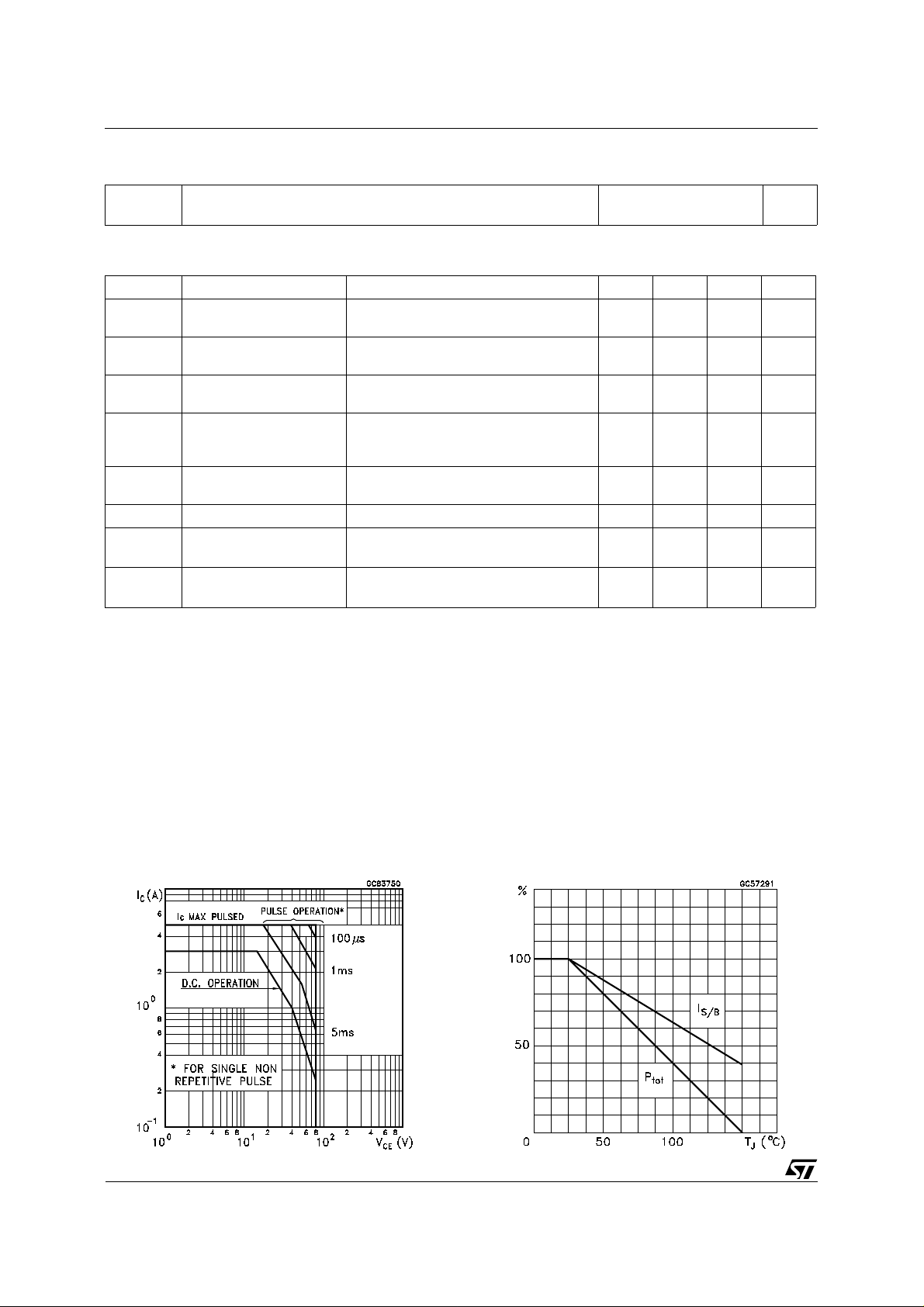
Safe Operating Are a Derating Curves
2/5
Page 3

MJB32B
DC Current Gain
Collector-Bas e Capacitance
Collector-Emitt er Sat uration Volta ge
3/5
Page 4

MJB32B
TO-263 (D2PAK) MECHANICAL DATA
DIM.
mm inch
MIN. TYP. MAX. MIN. TYP. MAX.
A 4.40 4.60 0.173 0.181
A1 2.49 2.69 0.098 0.106
A2 0.03 0.23 0.001 0.009
B 0.70 0.93 0.027 0.036
B2 1.14 1.70 0.044 0.067
C 0.45 0.60 0.017 0.023
C2 1.23 1.36 0.048 0.053
D 8.95 9.35 0.352 0.368
D1 8.00 0.315
E 10.00 10.40 0.393 0.409
E1 8.50 0.334
G 4.88 5.28 0.192 0.208
L 15.00 15.85 0.590 0.624
L2 1.27 1.4 0.050 0.055
L3 1.40 1.75 0.055 0.068
M 2.40 3.2 0.094 0.126
R 0.40 0.016
V2 0
o
o
8
o
0
o
8
- Weight : 1.38 g (typ.)
- The planaty of the slug must be within 30 µm
4/5
P011P6/G
Page 5

MJB32B
Information furnished is believed to be accurate and reliable. However, STMicroelectronics assumes no responsibility for the consequences
of use of such inform ation nor for any infringe ment o f patents or other rig hts o f third par ties which ma y resul t from i ts use. N o li cen se is
granted by implicatio n or otherwise under any patent or patent rights of STMicroelectronics. Specification mentioned in this publication are
subject to change without notice. This publication supersedes and replaces all information previously supplied. STMicroelectronics products
are not authorized for use as critical compo nents in life support devices or systems without express written approval of STMicroelectronics.
The ST logo is a trademark of STMicroelectronics
© 2001 STMicroelectro nics – Printed in Italy – All Rights Reserved
STMicroelectronics GROUP OF COMPANIES
Australia - Brazil - China - Finland - France - Germany - Hong Kong - India - Italy - Japan - Malaysia - Malta - Morocco -
Singapore - Spain - Sweden - Switzerland - United Kingdom - U.S.A.
http://www.st.com
5/5
 Loading...