

Page 1
2N3055
®
MJ2955
COMPLEMENTARY SILICON POWER TRANSISTORS
■
STMicroelectronics PREFERRED
SALESTYPES
■
COMPLEMENT A RY NPN-P NP DEVICES
DESCRIPTION
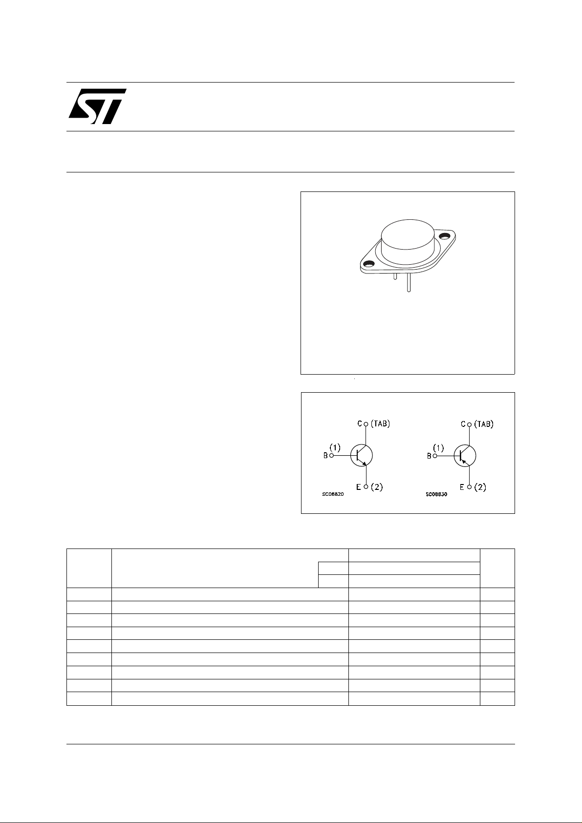
The 2N3055 is a silicon Epitaxial-Base Planar
NPN transistor mounted in Jedec TO-3 metal
case.
It is intended for power switching circuits, series
and shunt regulators, output stages and high
fidelity amplifiers.
The complementary PNP type is MJ2955.
1
2
TO-3
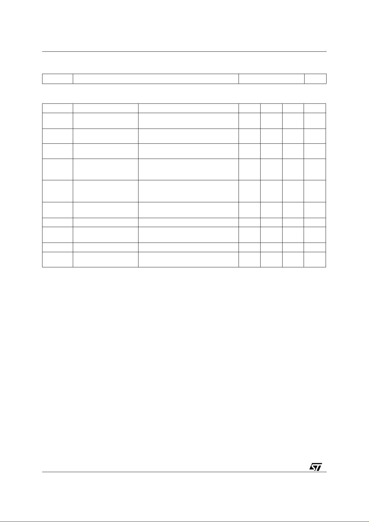
INTERNAL SCHEMATIC DIAGRAM
ABSOLUTE MAXIMUM RATINGS
Symbol Parameter Value Unit
NPN 2N3055
PNP MJ2955
V
V
V
V
P
T
For PNP types voltage and current values are negative.
Collector-Base Voltage (IE = 0) 100 V
CBO
Collector-Emitter Voltage (R
CER
Collector-Emitter Voltage (IB = 0) 60 V
CEO
Emitter-Base Voltage (IC = 0) 7 V
EBO
Collector Current 15 A
I
C
Base Current 7 A
I
B
Total Dissipation at Tc ≤ 25 oC
tot
Storage Temperature -65 to 200
stg
Max. Operating Junction Temperature 200
T
j
≤ 100Ω
BE
)
70 V
115 W
o
C
o
C
August 1999
1/4
Page 2
2N3055 / MJ2955
THERMAL DATA
R
thj-case
Thermal Resistance Junction-case Max 1.5
o
C/W
ELECTRICAL CHARACTERISTICS
= 25 oC unless otherwise specified)
(T
case
Symbol Parameter Test Conditions Min. Typ. Max. Unit
I
CEX
I
CEO
I
EBO
V
CEO(sus)
Collector Cut-off
Current (V
= -1.5V)
BE
Collector Cut-off
Current (I
= 0)
B
Emitter Cut-off Current
(I
= 0)
C
∗ Collector-Emitter
= 100 V
V
CE
V
= 100 V Tj = 150 oC
CE
= 30 V 0.7 mA
V
CE
= 7 V 5 mA
V
EB
I
= 200 mA 60 V
C
1
5
Sustaining Voltage
(I
= 0)
B
V
CER(sus)
∗ Collector-Emitter
IC = 200 mA 70 V
Sustaining
Voltage (R
V
∗ Collector-Emitter
CE(sat)
Saturation Voltage
V
∗ Base-Emitter Voltage I
BE
h
∗ DC Current Gain I
FE
f
I
s/b
Transition frequency IC = 0.5 A VCE = 10 V 3 MHz
T
∗ Second Breakdown
= 100 Ω)
BE
= 4 A IB = 400 mA
I
C
I
= 10 A IB = 3.3 A
C
= 4 A VCE = 4 A 1.8 V
C
= 4 A VCE = 4 A
C
I
= 10 A VCE = 4 A
C
= 40 V 2.87 A
V
CE
20
5
1
3
70
Collector Current
∗
Pulsed: Pulse duration = 300 µs, duty cycle 1.5 %
For PNP types voltage and current values are negative.
mA
mA
V
V
2/4
Page 3

TO-3 MECHANICAL DATA
2N3055 / MJ2955
DIM.
MIN. TYP. MAX. MIN. TYP. MAX.
A 11.00 13.10 0.433 0.516
B 0.97 1.15 0.038 0.045
C 1.50 1.65 0.059 0.065
D 8.32 8.92 0.327 0.351
E 19.00 20.00 0.748 0.787
G 10.70 11.10 0.421 0.437
N 16.50 17.20 0.649 0.677
P 25.00 26.00 0.984 1.023
R 4.00 4.09 0.157 0.161
U 38.50 39.30 1.515 1.547
V 30.00 30.30 1.187 1.193
mm inch
P
A
G
U
V
N
O
B
D
C
E
R
P003F
3/4
Page 4

2N3055 / MJ2955
Information f urnished i s believed t o be accurate an d reliabl e. How ever, STMicroelect ronics assu mes no responsib ility fo r the consequen ces
of use of such information nor for any infringement of patents or other rights of third parties which may result from its use. No license is
granted by implication or otherwise under any patent or patent rights of STMicroelectronics. Specification mentioned in this publication are
subject to chan ge w ithout notice. This publicatio n su persedes a nd r eplaces al l inf ormati on previ ously suppl ied. STMicroelect ron ics produ cts
are not auth ori zed f or use as critical component s in life support devices or systems without exp ress writ te n approval of STMicroelectronics.
The ST logo is a trademark of STMicroelectronics
© 1999 STMicroelectronics – Prin ted in Italy – All Rights Reserv ed
STMicroele ct ronics GROUP OF COMPANIES
Australia - Brazil - Canada - China - France - Germany - Italy - Japan - Korea - Malaysia - Malta - Mexico - Morocco - The Netherlands -
4/4
Singapore - Spain - Swed en - Switzerland - Taiwan - Thailand - United Kingdom - U.S. A.
http://www.st.com
.
 Loading...