

Page 1
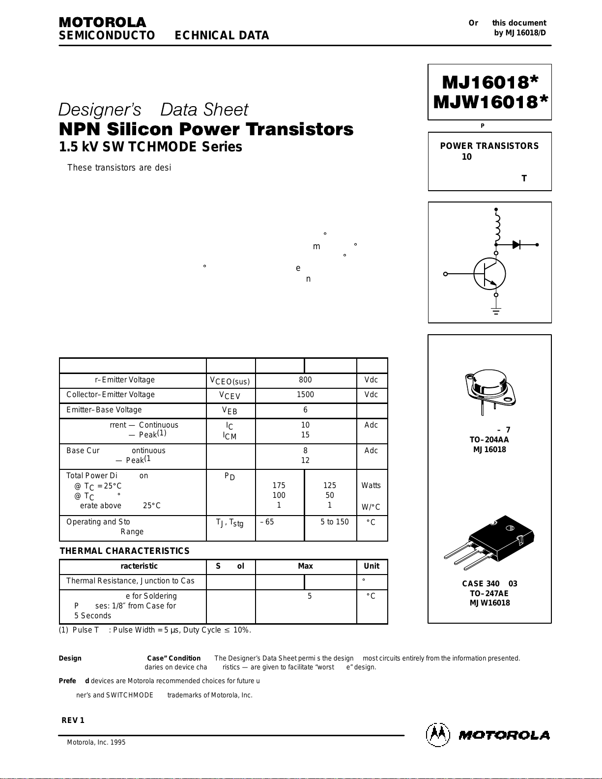
1
Motorola Bipolar Power Transistor Device Data
1.5 kV SWITCHMODE Series
These transistors are designed for high–voltage, high–speed, power switching in
inductive circuits where fall time is critical. T hey a re particularly s uited f or
line–operated switchmode applications.
Typical Applications: Features:
• Switching Regulators • Collector–Emitter Voltage — V
CEV
= 1500 Vdc
• Inverters • Fast Turn–Off Times
• Solenoids 80 ns Inductive Fall Time — 100_C (Typ)
• Relay Drivers 110 ns Inductive Crossover Time — 100_C (Typ)
• Motor Controls 4.5 µs Inductive Storage Time — 100_C (Typ)
• Deflection Circuits • 100_C Performance Specified for:
Reverse–Biased SOA with Inductive Load
Switching Times with Inductive Loads
Saturation Voltages
Leakage Currents
MAXIMUM RATINGS
Rating
Symbol
MJ16018
MJW16018
Unit
Collector–Emitter Voltage
V
CEO(sus)
800
Vdc
Collector–Emitter Voltage
V
CEV
1500
Vdc
Emitter–Base Voltage
V
EB
6
Vdc
Collector Current — Continuous
— Peak
(1)
I
C
I
CM
10
15
Adc
Base Current — Continuous
— Peak
(1)
I
B
I
BM
8
12
Adc
Total Power Dissipation
@ TC = 25_C
@ TC = 100_C
Derate above TC = 25_C
P
D
175
100
1
125
50
1
Watts
W/_C
Operating and Storage Junction
Temperature Range
TJ, T
stg
–65 to 200
–55 to 150
_
C
THERMAL CHARACTERISTICS
Characteristic
Symbol
Max
Unit
Thermal Resistance, Junction to Case
R
θJC
1
1
_
C/W
Lead Temperature for Soldering
Purposes: 1/8″ from Case for
5 Seconds
T
L
275
_
C
(1) Pulse Test: Pulse Width = 5 µs, Duty Cycle v 10%.
Designer’s Data for “Worst Case” Conditions — The Designer’s Data Sheet permits the design of most circuits entirely from the information presented. SOA Limit
curves — representing boundaries on device characteristics — are given to facilitate “worst case” design.
Preferred devices are Motorola recommended choices for future use and best overall value.
Designer’s and SWITCHMODE are trademarks of Motorola, Inc.
SEMICONDUCTOR TECHNICAL DATA
Order this document
by MJ16018/D
Motorola, Inc. 1995
POWER TRANSISTORS
10 AMPERES
800 VOLTS
125 AND 175 WATTS
*Motorola Preferred Device
CASE 1–07
TO–204AA
MJ16018
CASE 340F–03
TO–247AE
MJW16018
REV 1
Page 2
2
Motorola Bipolar Power Transistor Device Data
ELECTRICAL CHARACTERISTICS (T
C
= 25_C unless otherwise noted)
Characteristic
Symbol
Min
Typ
Max
ÎÎÎ
ÎÎÎ
ÎÎÎ
Unit
OFF CHARACTERISTICS
(1)
Collector–Emitter Sustaining Voltage (Table 1) (IC = 50 mA, IB = 0)
V
CEO(sus)
800
—
—
ÎÎÎ
ÎÎÎ
ÎÎÎ
Vdc
Collector Cutoff Current
(V
CEV
= 1500 Vdc, V
BE(off)
= 1.5 Vdc)
(V
CEV
= 1500 Vdc, V
BE(off)
= 1.5 Vdc, TC = 100_C)
I
CEV
—
—
—
—
0.25
1.5
ÎÎÎ
ÎÎÎ
ÎÎÎ
ÎÎÎ
mAdc
Collector Cutoff Current (VCE = 1500 Vdc, RBE = 50 Ω, TC = 100_C)
I
CER
—
—
2.5
ÎÎÎ
ÎÎÎ
ÎÎÎ
mAdc
Emitter Cutoff Current (VEB = 6 Vdc, IC = 0)
I
EBO
—
—
0.1
ÎÎÎ
ÎÎÎ
ÎÎÎ
mAdc
SECOND BREAKDOWN
Second Breakdown Collector Current with Base Forward Biased
I
S/b
See Figure 13
Clamped Inductive SOA with Base Reverse Biased
RBSOA
See Figure 14
ON CHARACTERISTICS
(1)
Collector–Emitter Saturation Voltage
(IC = 5 Adc, IB = 2 Adc)
(IC = 10 Adc, IB = 5 Adc)
(IC = 5 Adc, IB = 2 Adc, TC = 100_C)
V
CE(sat)
—
—
—
—
—
—
1
5
1.5
ÎÎÎ
ÎÎÎ
ÎÎÎ
ÎÎÎ
ÎÎÎ
Vdc
Base–Emitter Saturation Voltage (IC = 5 Adc, IB = 2 Adc)
Base–Emitter Saturation Voltage (IC = 5 Adc, IB = 2 Adc, TC = 100_C)
V
BE(sat)
—
—
—
—
1.5
1.5
ÎÎÎ
ÎÎÎ
ÎÎÎ
Vdc
DC Current Gain (IC = 5 Adc, VCE = 5 Vdc)
h
FE
4
—
—
ÎÎÎ
ÎÎÎ
ÎÎÎ
—
DYNAMIC CHARACTERISTICS
Output Capacitance (VCB = 10 Vdc, IE = 0, f
test
= 1 kHz)
C
ob
—
—
450
ÎÎÎ
ÎÎÎ
ÎÎÎ
pF
SWITCHING CHARACTERISTICS
Inductive Load (Table 1)
Storage Time
t
sv
—
4000
8000
ÎÎÎ
ÎÎÎ
ÎÎÎ
Fall Time
_
C)
t
fi
—
60
200
ÎÎÎ
ÎÎÎ
ÎÎÎ
Crossover Time
(IC = 5 Adc,
IB1 = 2 Adc,
J
= 25_C)
t
c
—
90
300
ÎÎÎ
ÎÎÎ
ÎÎÎ
Storage Time
B1
= 2 Adc,
V
BE(off)
= 2 Vdc,
t
sv
—
4500
9000
ÎÎÎ
ÎÎÎ
ÎÎÎ
Fall Time
V
CE(pk)
= 400 Vdc)
PW = 25 µs
_
C)
t
fi
—
80
250
ÎÎÎ
ÎÎÎ
ÎÎÎ
Crossover Time
PW = 25 µs
J
= 100_C)
t
c
—
110
375
ÎÎÎ
ÎÎÎ
ÎÎÎ
Resistive Load (Table 1)
Delay Time
t
d
—
85
200
ÎÎÎ
ÎÎÎ
ÎÎÎ
Rise Time
t
r
—
900
2000
ÎÎÎ
ÎÎÎ
ÎÎÎ
Storage Time
IB1 = 2 Adc, IB2 = 2 Adc,
RB2 = 3 Ω, PW = 25 µs,
t
s
—
4500
9000
ÎÎÎ
ÎÎÎ
ÎÎÎ
Fall Time
RB2 = 3 Ω, PW = 25 µs,
Duty Cycle v 2%)
t
f
—
200
400
ÎÎÎ
ÎÎÎ
ÎÎÎ
(1) Pulse Test: PW = 300 µs, Duty Cycle v 2%.
V
CE
, COLLECTOR–EMITTER VOLTAGE (VOLTS)
IC = 1 A
100
0.2
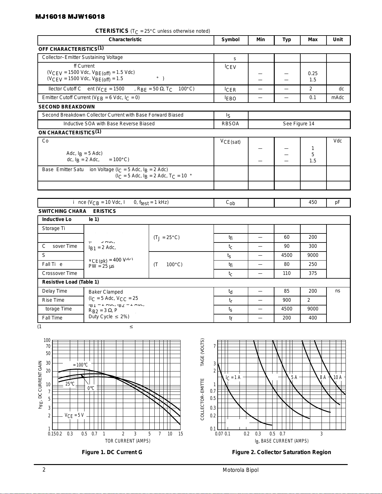
Figure 1. DC Current Gain
IC, COLLECTOR CURRENT (AMPS)
1
0.5 3 10 15
10
7
Figure 2. Collector Saturation Region
0.07
IB, BASE CURRENT (AMPS)
1
0.2 0.7
7
3
2
70
h
FE
, DC CURRENT GAIN
3
VCE = 5 V
1 2 5 7
10
5
TC = 25°C
3 A
TC = 100°C
0°C
25°C
30
1 7
50
20
5
2
0.3 0.7 20.15 5 0.3 0.5 3
0.1
0.7
0.3
0.2
0.5
10 A
0.1
5 A 8 A
Baker Clamped
(TJ = 25
(TJ = 100
Baker Clamped
(IC = 5 Adc, VCC = 250 Vdc,
ns
ns
Page 3
3
Motorola Bipolar Power Transistor Device Data
C, CAPACITANCE (pF)
V
BE
, BASE–EMITTER VOLTAGE (VOLTS)
V
CE
, COLLECTOR–EMITTER VOLTAGE (VOLTS)
0.1
IC, COLLECTOR CURRENT (AMPS)
0.2 1
5
1
0.7
0.5
10
IC, COLLECTOR CURRENT (AMPS)
7
5
1
0.5
0.2
0.2
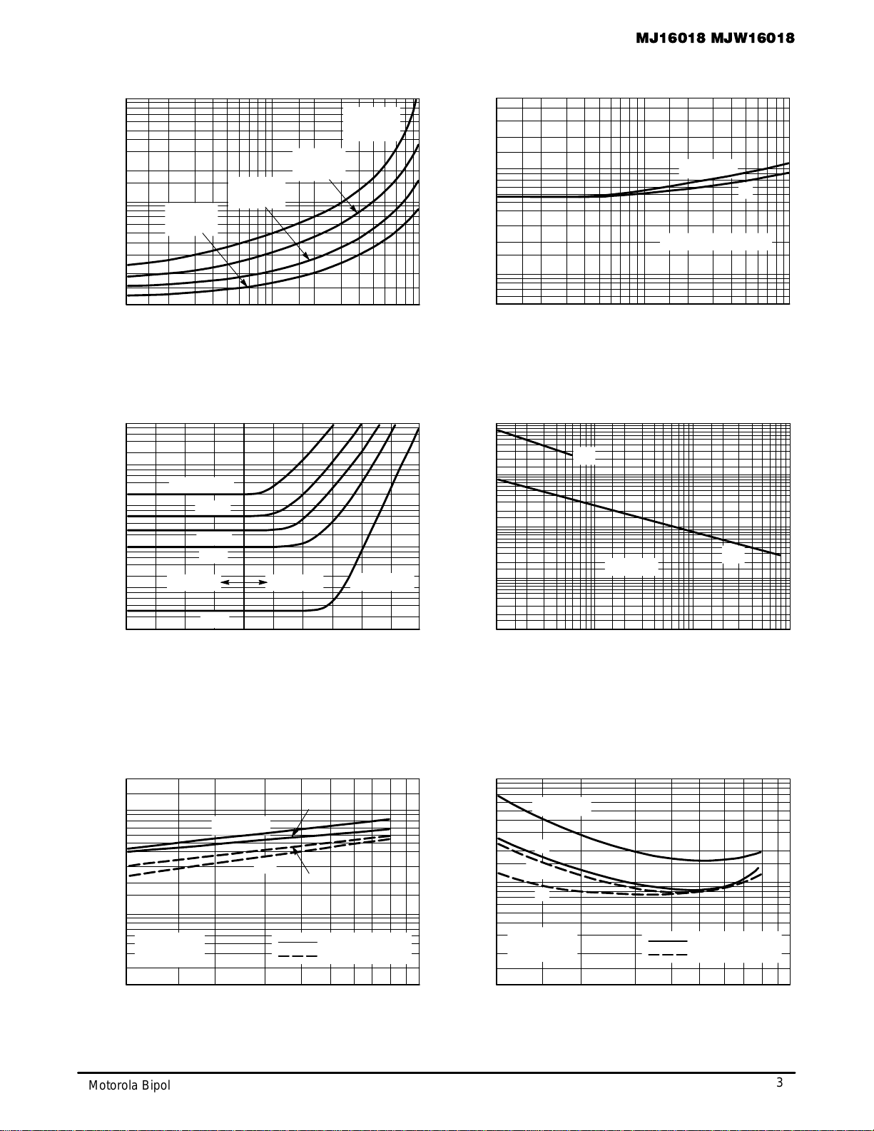
Figure 3. Collector–Emitter Saturation Region
50.50.1 0.2 0.3 1 103 7
Figure 4. Base–Emitter Saturation Region
Figure 5. Collector Cutoff Region
10
4
VBE, BASE–EMITTER VOLTAGE (VOLTS)
10
–1
0
0.1
IC/IB = 2.5
TC = 25
°
C
2 10
–0.4
Figure 6. Typical Capacitance
10K
VCB, COLLECTOR–BASE VOLTAGE (VOLTS)
TC = 25°C
C
ib
1
, COLLECTOR CURRENT ( A)
µ
I
C
0.3
TC = 25°C THRU 100°C
10
3
10
2
10
1
10
0
–0.2 +0.2 +0.4 +0.6
TJ = 150°C
125°C
100°C
75°C
REVERSE FORWARD
25°C
VCE = 250 V
1K
100
1
2 5 10 20 50 100 200 500 1K
IC/IB = 2.5
TC = 100
°
C
IC/IB = 5
TC = 25
°
C
IC/IB = 5
TC = 100
°
C
0.5 0.7 52
5
IC/IB = 2.5
0.1
0.05
0.07
3
2
10
3
2
0.7
0.3
0.3 0.7 3 7
C
ob
TYPICAL STATIC CHARACTERISTICS
t
fi
, FALL TIME (ns)
Figure 7. Storage Time Figure 8. Inductive Switching Fall Time
IC, COLLECTOR CURRENT (AMPS)
2 3 5 7 10
0.2
, STORAGE TIME ( s)t
sv
1
IC, COLLECTOR CURRENT (AMPS)
2 3 5 7 10
1000
500
200
70
30
10
1
V
BE(off)
= 2 V
TC = 100
°
C
700
300
100
50
20
NO BAKER CLAMP
BAKER CLAMPED
NO BAKER CLAMP
BAKER CLAMPED
V
BE(off)
= 2 V
TC = 100
°
C
IC/IB = 2.5
2.5
20
7
3
1
0.5
10
5
2
0.7
0.3
µ
5
5
IC/IB = 2.5
5
5
2.5
TYPICAL INDUCTIVE SWITCHING CHARACTERISTICS
Page 4
4
Motorola Bipolar Power Transistor Device Data
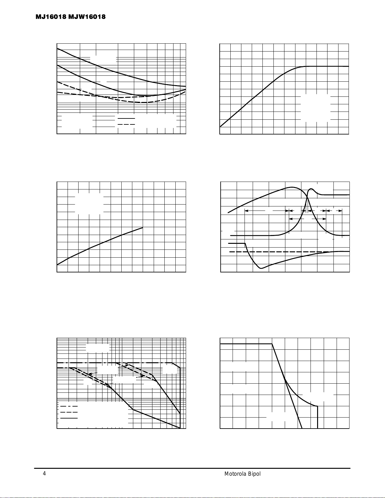
Figure 9. Inductive Switching Crossover Time Figure 10. (tsv) Storage Time versus I
B1
Pulse Width
IC, COLLECTOR CURRENT (AMPS)
2 3 5 7 101
V
BE(off)
= 2 V
TC = 100
°
C
NO BAKER CLAMP
BAKER CLAMPED
Figure 11. Reverse Base Current versus
Off Voltage
VOLTAGE AND CURRENT
IC, COLLECTOR CURRENT (AMPS)
2000
1000
500
100
50
20
PULSE WIDTH (
µ
s)
5 9 13 17 21
6
5
4
3
2
0
1
1
IC = 5 A
IB1 = 2 A
IB2 = 2 A OR
VBE = –2 V
Figure 12. Inductive Switching Measurements
700
300
200
70
30
25
I
B2
, REVERSE BASE CURRENT (AMPS)
V
BE(off)
, REVERSE BASE–EMITTER VOLTAGE (VOLTS)
6
5
–1 –2 –3 –4
4
3
2
1
IC = 5 A
IB1 = 2 A
VCE = 400 V
–5 –6
t
c
, CROSSOVER TIME (ns)
, STORAGE TIME ( s)t
sv
µ
IC/IB = 2.5
2.5
5
5
t
fi
t
rv
TIME
I
C
90% I
B1
IC pk
V
CE(pk)
90% V
CE(pk)
90% I
C(pk)
10% V
CE(pk)
10%
IC pk
2% I
C
I
B
t
sv
t
ti
t
c
V
CE
TYPICAL INDUCTIVE SWITCHING CHARACTERISTICS
I
C(pk)
, PEAK COLLECTOR CURRENT (AMPS)
10
I
C
, COLLECTOR CURRENT (AMPS)
Figure 13. Maximum Forward Bias
Safe Operating Area
Figure 14. Maximum Reverse Bias
Safe Operating Area
100
10
VCE, COLLECTOR–EMITTER VOLTAGE (VOLTS)
0.1
15 1K
30
20
2
50
1
0.5
0.3
0.2
BONDING WIRE LIMIT
THERMAL LIMIT
SECOND BREAKDOWN
LIMIT
20 50 100 200 500
TC = 25°C
10µs
1 ms
dc
5
3
MJ16018
MJW16018
30 300
16
V
CE(pk)
, PEAK COLLECTOR VOLTAGE (VOLTS)
0
2K
12
8
4
400 800 1.8K1K 1.6K
V
BE(off)
= 0 V
0 1.2K200 600 1.4K
14
10
6
2
V
BE(off)
= 2 V
IC/IB1 = 2.5, 5
TC ≤ 100°C
GUARANTEED SAFE OPERATING AREA LIMITS
Page 5
5
Motorola Bipolar Power Transistor Device Data
POWER DERATING FACTOR (%)
100
0
TC, CASE TEMPERATURE (
°
C)
0
40 200
80
60
40
20
MJ16018
MJW16018
80 120 160
Figure 15. Power Derating
SECOND BREAKDOWN
DERATING
THERMAL
DERATING
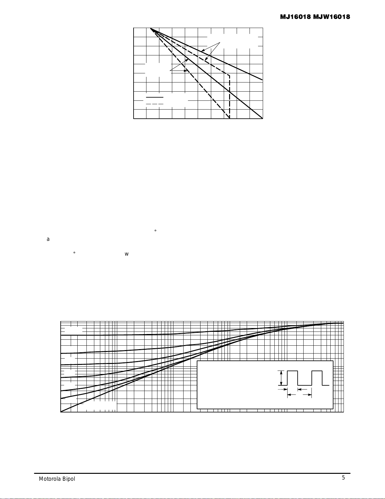
SAFE OPERATING AREA INFORMATION
FORWARD BIAS
There are two limitations on the power handling ability of a
transistor: average junction temperature and second breakdown. Safe operating area curves indicate IC – VCE limits of
the transistor that must be observed for reliable operation;
i.e., the transistor must not be subjected to greater dissipation than the curves indicate.
The data of Figure 13 is based on TC = 25_C; T
J(pk)
is
variable depending on power level. Second breakdown pulse
limits are valid for duty cycles to 10% but must be derated
when TC ≥ 25_C. Second breakdown limitations do not derate the same as thermal limitations. Allowable current at the
voltages shown on Figure 13 may be found at any case temperature by using the appropriate curve on Figure 15.
T
J(pk)
may be calculated from the data in Figure 16. At
high case temperatures, thermal limitations will reduce the
power that can be handled to values less than the limitations
imposed by second breakdown.
REVERSE BIAS
For inductive loads, high voltage and high current must be
sustained simultaneously during turn–off, in most cases, with
the base–to–emitter junction reverse biased. Under these
conditions the collector voltage must be held to a safe level
at or below a specific value of collector current. This can be
accomplished by several means such as active clamping,
RC snubbing, load line shaping, etc. The safe level for these
devices is specified as Reverse Bias Safe Operating Area
and represents the voltage current condition allowable during r everse biased turnoff. This rating is verified u nder
clamped conditions so that the device is never subjected to
an avalanche mode. Figure 14 gives the RBSOA characteristics.
t, TIME (ms)
1.0
0.01
0.01
0.7
0.2
0.1
0.05
0.02
r(t), TRANSIENT THERMAL RESISTANCE (NORMALIZED)
1.0 2.0 5.0 10 20 50 100 200 500
R
θ
JC
(t) = r(t) R
θ
JC
R
θ
JC
= 1.0
°
C/W MAX
D CURVES APPLY FOR POWER
PULSE TRAIN SHOWN
READ TIME @ t
1
T
J(pk)
– TC = P
(pk)
R
θ
JC
(t)
P
(pk)
t
1
t
2
DUTY CYCLE, D = t1/t
2
D = 0.5
0.2
0.01
SINGLE PULSE
0.1
0.1 0.50.2 1.0 k
Figure 16. Thermal Response
0.5
0.3
0.07
0.03
0.02 0.05
0.02
0.05
Page 6
6
Motorola Bipolar Power Transistor Device Data
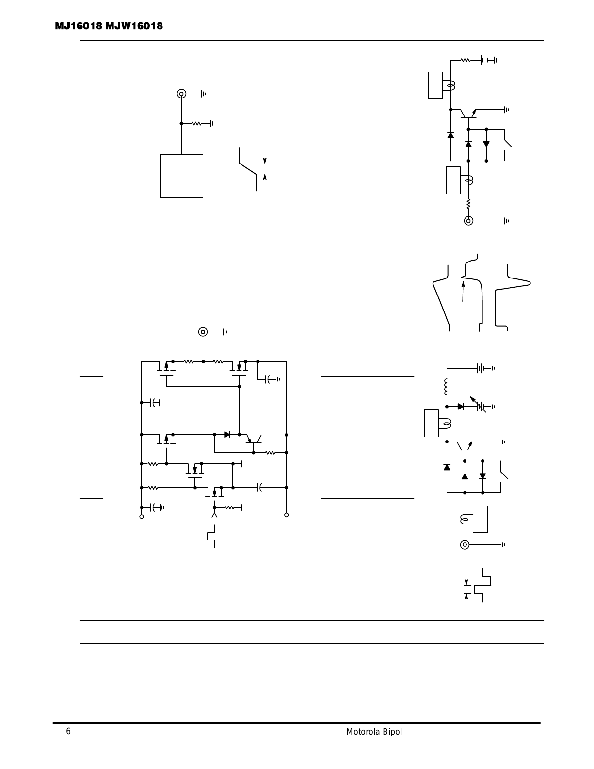
Resistive SwitchingInductive SwitchingRBSOAV
CEO(sus)
Input
Conditions
Circuit
Values
Test Circuit
Table 1. Test Conditions for Dynamic Performance
+15
1 F
µ
100 F
µ
500 F
µ
150
Ω
100
Ω
V
off
+10
50
Ω
150
Ω
MUR105
MJE210
1 F
µ
MTP12N10
MTP8P10
MTP8P10
A
R
B1
R
B2
Note: Adjust V
off
to obtain desired V
BE(off)
at Point A
Drive Circuit
For t
d
and t
f
:
H.P. 214OREQUIV.
P.G.
50
Ω
A
0
V
in
t
r
15 ns
≤
≈
11 V
For t
s
and t
f
:
Inductive Switching Drive
Circuit
L = 10 mH
R
B2
=
V
CC
= 20 Volts
I
(pk)
= 50 mA
S
1
Closed
∞
L = 200
R
B2
= 0
V
CC
= 20 Volts
S
1
Closed
µ
H
R
B1
selected for
desired I
B1
L = 200
R
B2
= 0 when V
µ
H
BE(off)
is specified or
selected for desired I
B2
V
CC
≈
20 Volts, Adjusted to obtain
desired IC
R
B1
selected for desired I
B1
S
1
= Open for baker
clamp condition
V
CC
= 250 Volts
R
B
selected for desired I
B1
R
L
selected for desired I
C
for t
d
and t
r
V
CC
= 250 Volts
for t
s
and t
f
R
B
= 0
R
B1
selected for I
B1
& R
B2
& I
B2
R
L
selected for desired I
C
T
1
0 V
+V
–V
A
MUR1100
MUR105
MUR105
T.U.T.
L
MUR8100
V
CC
V
clamp
S
1
*I
C
*I
B
V
CE
I
B
I
C
I
B1
I
B2
I
C(pk)
V
CE(pk)
A
R
B
*I
C
*I
B
S
1
MUR105
MUR105
MUR1100
T.U.T.
R
L
V
CC
*Tektronix AM503
P6302 or Equivalent
Scope — Tektronix
7403 or Equivalent
*Tektronix AM503
P6302 or Equivalent
T
1
adjusted to obtain I
C(pk)
T
1
≈
L
coil
(I
Cpk
)
V
CC
Page 7
7
Motorola Bipolar Power Transistor Device Data
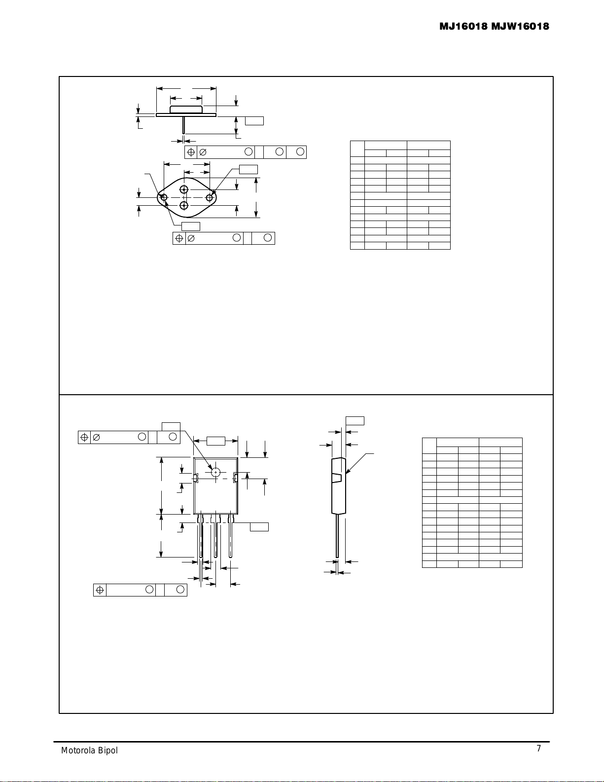
PACKAGE DIMENSIONS
NOTES:
1. DIMENSIONING AND TOLERANCING PER ANSI
Y14.5M, 1982.
2. CONTROLLING DIMENSION: INCH.
3. ALL RULES AND NOTES ASSOCIATED WITH
REFERENCED TO–204AA OUTLINE SHALL APPLY.
STYLE 1:
PIN 1. BASE
2. EMITTER
CASE: COLLECTOR
DIM MIN MAX MIN MAX
MILLIMETERSINCHES
A 1.550 REF 39.37 REF
B ––– 1.050 ––– 26.67
C 0.250 0.335 6.35 8.51
D 0.038 0.043 0.97 1.09
E 0.055 0.070 1.40 1.77
G 0.430 BSC 10.92 BSC
H 0.215 BSC 5.46 BSC
K 0.440 0.480 11.18 12.19
L 0.665 BSC 16.89 BSC
N ––– 0.830 ––– 21.08
Q 0.151 0.165 3.84 4.19
U 1.187 BSC 30.15 BSC
V 0.131 0.188 3.33 4.77
A
N
E
C
K
–T–
SEATING
PLANE
2 PLD
M
Q
M
0.13 (0.005) Y
M
T
M
Y
M
0.13 (0.005) T
–Q–
–Y–
2
1
U
L
G
B
V
H
CASE 1–07
TO–204AA (TO–3)
ISSUE Z
CASE 340F–03
TO–247AE
ISSUE E
DIMAMIN MAX MIN MAX
INCHES
20.40 20.90 0.803 0.823
MILLIMETERS
B 15.44 15.95 0.608 0.628
C 4.70 5.21 0.185 0.205
D 1.09 1.30 0.043 0.051
E 1.50 1.63 0.059 0.064
F 1.80 2.18 0.071 0.086
G 5.45 BSC 0.215 BSC
H 2.56 2.87 0.101 0.113
J 0.48 0.68 0.019 0.027
K 15.57 16.08 0.613 0.633
L 7.26 7.50 0.286 0.295
P 3.10 3.38 0.122 0.133
Q 3.50 3.70 0.138 0.145
R 3.30 3.80 0.130 0.150
U 5.30 BSC 0.209 BSC
V 3.05 3.40 0.120 0.134
NOTES:
1. DIMENSIONING AND TOLERANCING PER ANSI
Y14.5M, 1982.
2. CONTROLLING DIMENSION: MILLIMETER.
STYLE 3:
PIN 1. BASE
2. COLLECTOR
3. EMITTER
4. COLLECTOR
R
P
A
K
V
F
D
G
U
L
E
0.25 (0.010)MT B
M
0.25 (0.010)MY Q
S
J
H
C
4
1 2 3
–T–
–B–
–Y–
–Q–
Page 8
8
Motorola Bipolar Power Transistor Device Data
How to reach us:
USA /EUROPE: Motorola Literature Distribution; JAPAN: Nippon Motorola Ltd.; Tatsumi–SPD–JLDC, Toshikatsu Otsuki,
P.O. Box 20912; Phoenix, Arizona 85036. 1–800–441–2447 6F Seibu–Butsuryu–Center, 3–14–2 Tatsumi Koto–Ku, Tokyo 135, Japan. 03–3521–8315
MFAX: RMFAX0@email.sps.mot.com – TOUCHTONE (602) 244–6609 HONG KONG: Motorola Semiconductors H.K. Ltd.; 8B Tai Ping Industrial Park,
INTERNET: http://Design–NET.com 51 Ting Kok Road, Tai Po, N.T., Hong Kong. 852–26629298
Motorola reserves the right to make changes without further notice to any products herein. Motorola makes no warranty , representation or guarantee regarding
the suitability of its products for any particular purpose, nor does Motorola assume any liability arising out of the application or use of any product or circuit,
and specifically disclaims any and all liability, including without limitation consequential or incidental damages. “T ypical” parameters can and do vary in different
applications. All operating parameters, including “T ypicals” must be validated for each customer application by customer’s technical experts. Motorola does
not convey any license under its patent rights nor the rights of others. Motorola products are not designed, intended, or authorized for use as components in
systems intended for surgical implant into the body, or other applications intended to support or sustain life, or for any other application in which the failure of
the Motorola product could create a situation where personal injury or death may occur. Should Buyer purchase or use Motorola products for any such
unintended or unauthorized application, Buyer shall indemnify and hold Motorola and its officers, employees, subsidiaries, affiliates, and distributors harmless
against all claims, costs, damages, and expenses, and reasonable attorney fees arising out of, directly or indirectly, any claim of personal injury or death
associated with such unintended or unauthorized use, even if such claim alleges that Motorola was negligent regarding the design or manufacture of the part.
Motorola and are registered trademarks of Motorola, Inc. Motorola, Inc. is an Equal Opportunity/Affirmative Action Employer.
MJ16018/D
*MJ16018/D*
◊
 Loading...