

Page 1
MIC79050 Micrel
4.2V ±0.75%
Li-Ion
Cell
IN BAT
FB
GND
EN
MIC79050-4.2BMM
External PWM*
*See Applications Information
Regulated or
unregulated
wall adapter
MIC79050
Simple Lithium-Ion Battery Charger
Preliminary Information
General Description
The MIC79050 is a simple single-cell lithium-ion battery
charger. It includes an on-chip pass transistor for high precision charging. Featuring ultrahigh precision (+0.75% over the
Li-ion battery charging temperature range) and “zero” off
mode current, the MIC79050 provides a very simple, cost
effective solution for charging lithium-ion battery.
Other features of the MIC79050 include current limit and
thermal shutdown protection. In the event the input voltage to
the charger is disconnected, the MIC79050 also provides
minimal reverse-current and reversed-battery protection.
The MIC79050 is a fixed 4.2V device and comes in the
thermally-enhanced MSO-8, SO-8, and SOT-223 packages.
The 8-pin versions also come equipped with enable and
feedback inputs. All versions are specified over the temperature range of –40°C to +125°C.
Ordering Information
Part Number Voltage Junct. Temp. Range Package
MIC79050-4.2BS 4.2V –40°C to +125°C SOT-223
MIC79050-4.2BM 4.2V –40°C to +125°C SOP-8
MIC79050-4.2BMM 4.2V –40°C to +125°C MSOP-8
Features
• High accuracy charge voltage:
±0.75% over -5°C to + 60°C (Li-ion charging
temperature range)
• “Zero” off-mode current
•10µA reverse leakage
• Ultralow 380mV dropout at 500mA
• Wide input voltage range
• Logic controlled enable input (8-pin devices only)
• Thermal shutdown and current limit protection
• Power MSOP-8, Power SOP-8, and SOT-223
• Pulse charging capability
Applications
• Li-ion battery charger
• Celluar phones
• Palmtop computers
• PDAs
• Self charging battery packs
Typical Applications
Regulated or
unregulated
wall adapter
MIC79050-4.2BS
IN BAT
GND
Simplest Battery Charging Solution
Pulse-Charging Application
Micrel, Inc. • 1849 Fortune Drive • San Jose, CA 95131 • USA • tel + 1 (408) 944-0800 • fax + 1 (408) 944-0970 • http://www.micrel.com
June 2000 1 MIC79050
4.2V ±0.75% Over Temp
Li-Ion
Cell
Page 2
MIC79050 Micrel
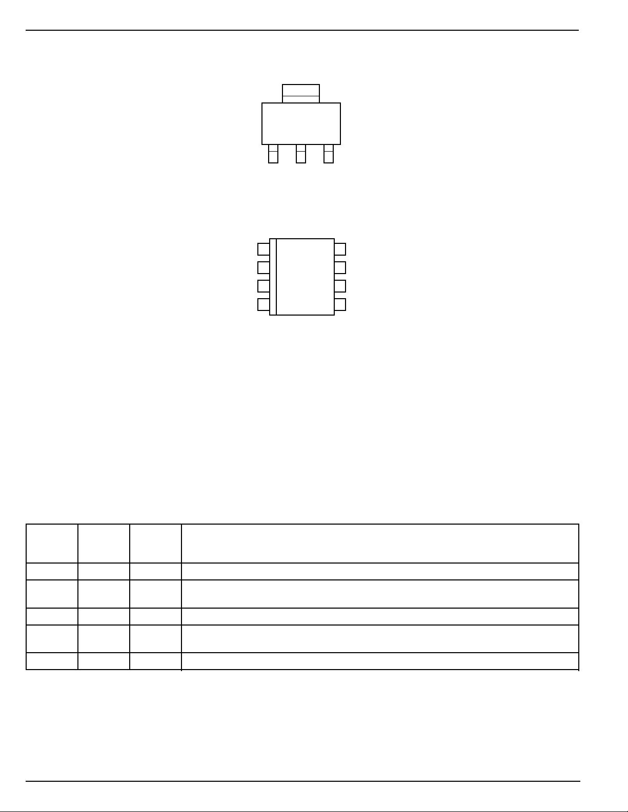
Pin Configuration
GND
TAB
132
IN
GND
BAT
MIC79050-x.xBS
SOT-223
EN
BAT
FB
IN
1
2
3
4
GND
8
GND
7
GND
6
GND
5
MIC79050-x.xBM
SOP-8 and MSOP-8
Pin Description
Pin No. Pin No. Pin Name Pin Function
SOT-223 SOP-8
MSOP-8
1 2 IN Supply Input
2,
TAB 5–8 GND Ground: SOT-223 pin 2 and TAB are internally connected. SO-8 pins 5 through 8 are
internally connected.
3 3 BAT Battery Voltage Output
1 EN Enable (Input): TTL/CMOS compatible control input. Logic high = enable; logic low or open =
shutdown.
4 FB Feedback Node
MIC79050 2 June 2000
Page 3

MIC79050 Micrel
Absolute Maximum Ratings (Note 1)
Supply Input Voltage (V
Power Dissipation (P
Junction Temperature (T
Lead Temperature (soldering, 5 sec.) ....................... 260°C
Storage Temperature (T
) ............................ –20V to +20V
IN
) ............... Internally Limited, Note 3
D
) ....................... –40°C to +125°C
J
) ....................... –65°C to +150°C
S
Operating Ratings (Note 2)
Supply Input Voltage (V
Enable Input Voltage (V
Junction Temperature (TJ) ....................... –40°C to +125°C
Package Thermal Resistance (Note 3) ...............................
MSOP-8 (θ
SOP-8(θ
)......................................................80°C/W
JA
)..........................................................63°C/W
JA
) ........................... +2.5V to +16V
IN
) .................................. 0V to V
EN
SOT-223(θJC)......................................................15°C/W
Electrical Characteristics
VIN = V
Symbol Parameter Conditions Min Typical Max Units
V
BAT
∆V
BAT
∆V
BAT/VBAT
∆V
BAT/VBAT
V
– V
IN
I
GND
I
GND
PSRR Ripple Rejection f = 120Hz 75 dB
I
LIMIT
∆V
BAT
ENABLE Input
V
ENL
I
ENL
I
ENH
BAT
+ 1.0V; C
Battery Voltage Accuracy variation from nominal V
= 4.7µF, I
OUT
= 100µA; TJ = 25°C, bold values indicate –40°C ≤ TJ ≤ +125°C; unless noted.
OUT
–5°C to +60°C –0.75 +0.75 %
OUT
/∆T Battery Voltage Note 4 40 ppm/°C
Temperature Coefficient
Line Regulation VIN = V
+ 1V to 16V 0.009 0.05 %/V
BAT
0.1 %/V
Load Regulation I
= 100µA to 500mA, Note 5 0.05 0.5 %
OUT
0.7 %
BAT
Dropout Voltage, Note 6 I
= 500mA 380 500 mV
OUT
600 mV
Ground Pin Current, Notes 7, 8 VEN ≥ 3.0V, I
= 100µA 85 130 µA
OUT
170 µA
V
≥ 3.0V, I
EN
= 500mA 11 20 mA
OUT
25 mA
Ground Pin Quiescent Current, VEN ≤ 0.4V (shutdown) 0.05 3 µA
Note 8
Current Limit V
VEN ≤ 0.18V (shutdown) 0.10 8 µA
= 0V 750 900 mA
BAT
1000 mA
/∆P
Thermal Regulation Note 9 0.05 %/W
D
Enable Input Logic-Low Voltage VEN = logic low (shutdown) 0.4 V
0.18 V
VEN = logic high (enabled) 2.0 V
Enable Input Current V
≤ 0.4V (shutdown) 0.01 –1 µA
ENL
V
≤ 0.18V (shutdown) 0.01 –2 µA
ENL
V
≥ 2.0V (enabled) 5 20 µA
ENH
25 µA
IN
Note 1. Exceeding the absolute maximum rating may damage the device.
Note 2. The device is not guaranteed to function outside its operating rating.
Note 3. The maximum allowable power dissipation at any TA (ambient temperature) is calculated using: P
maximum allowable power dissipation will result in excessive die temperature, and the regulator will go into thermal shutdown.
Note 4. Battery voltage temperature coefficient is the worst case voltage change divided by the total temperature range.
Note 5. Regulation is measured at constant junction temperature using low duty cycle pulse testing. Parts are tested for load regulation in the load
range from 100µA to 500mA. Changes in output voltage due to heating effects are covered by the thermal regulation specification.
Note 6. Dropout voltage is defined as the input to battery output differential at which the battery voltage drops 2% below its nominal value measured at
1V differential.
Note 7: Ground pin current is the charger quiescent current plus pass transistor base current. The total current drawn from the supply is the sum of the
load current plus the ground pin current.
D(max)
= (T
– TA) ÷ θJA. Exceeding the
J(max)
June 2000 3 MIC79050
Page 4

MIC79050 Micrel
Note 8: VEN is the voltage externally applied to devices with the EN (enable) input pin. [MSO-8(MM) and SO-8 (M) packages only.]
Note 9: Thermal regulation is the change in battery voltage at a time “t” after a change in power dissipation is applied, excluding load or line regulation
effects. Specifications are for a 500mA load pulse at V
= 16V for t = 10ms.
IN
MIC79050 4 June 2000
Page 5
MIC79050 Micrel
g
g
3.0
3.2
3.4
3.6
3.8
4.0
-40 0 40 80 120
GROUND CURRENT (mA)
TEMPERATURE (C)
Ground Current
vs. Temperature
0
100
200
300
400
500
600
700
800
-40 0 40 80 120
SHORT CIRCUIT CURRENT (mA)
TEMPERATURE (C)
Short Circuit Current
vs. Temperature
Typical Characteristics
Dropout Voltage
vs. Output Current
400
300
200
100
DROPOUT VOLTAGE (mV)
0
0 100 200 300 400 500
OUTPUT CURRENT (mA)
Dropout Characteristics
5
4
3
2
1
OUTPUT VOLTAGE (V)
0
0246
250mA
500mA
INPUT VOLTAGE (V)
Dropout Voltage
600
500
400
300
200
100
DROPOUT VOLTAGE (mV)
vs. Temperature
0
-40 0 40 80 120
TEMPERATURE (C)
Output Current
12
10
8
6
4
2
GROUND CURRENT (mA)
0
0 100 200 300 400 500
vs. Ground
OUTPUT CURRENT (mA)
Dropout Characteristics
5
4
3
2
1
OUTPUT VOLTAGE (V)
5mA
50mA, 150mA
0
0246810121416
INPUT VOLTAGE (V)
Ground Current
vs. Supply Volta
1.5
50mA
1
5mA
0.5
GROUND CURRENT (mA)
0
0 4 8 12 16
SUPPLY VOLTAGE (V)
e
vs. Supply Volta
25
20
15
10
5
GROUND CURRENT (mA)
0
0123456
SUPPLY VOLTAGE (V)
13.5
13.0
12.5
June 2000 5 MIC79050
12.0
11.5
GROUND CURRENT (mA)
11.0
-40 0 40 80 120
Ground Current
500mA
250mA
125mA
Ground Current
vs. Temperature
TEMPERATURE (C)
Ground Current
e
150
100
GROUND CURRENT (uA)
vs. Temperature
50
0
-40 0 40 80 120
TEMPERATURE (C)
Battery Voltage
4.210
4.205
4.200
4.195
OUTPUT VOLTAGE (V)
4.190
vs. Temperature
-40 -20 0 20 40 60 80 100120140
TEMPERATURE (C)
Page 6
MIC79050 Micrel
Typical Voltage Drift Limits
0.75
0.25
-0.25
-0.75
DRIFT FROM NOMINAL VOUT (%)
0 200 400 600 800
vs. Time
Upper
Lower
TIME (hrs)
Reverse Leakage Current
vs. Output Voltage
20
15
10
5
0
012345
REVERSE LEAKAGE CURRENT (µA)
OUTPUT VOLTAGE (V)
Reverse Leakage Current
vs. Temperature
20
4.2V
15
3.6V
10
3.0V
5
0
-5 5 1525354555
REVERSE LEAKAGE CURRENT (uA)
TEMPERATURE (C)
VIN+V
EN
GROUNDED
Reverse Leakage Current
vs. Output Voltage
20
4.2V
15
3.6V
10
3.0V
5
0
-5 5 1525354555
REVERSE LEAKAGE CURRENT (µA)
TEMPERATURE (C)
VIN+V
EN
FLOATING
MIC79050 6 June 2000
Page 7

MIC79050 Micrel
Block Diagrams
V
IN
IN
V
BAT
Bandgap
Ref.
Current Limit
Thermal Shutdown
MIC79050-x.xBS
GND
3-Pin Version
V
IN
IN
FB
V
BAT
EN
Current Limit
Thermal Shutdown
MIC79050-x.xBMM/M
5-Pin Version
Bandgap
Ref.
V
REF
GND
June 2000 7 MIC79050
Page 8

MIC79050 Micrel
Functional Description
The MIC79050 is a high-accuracy, linear battery charging
circuit designed for the simplest implementation of a single
lithium-ion (Li-ion) battery charger. The part can operate from
a regulated or unregulated power source, making it ideal for
various applications. The MIC79050 can take an unregulated
voltage source and provide an extremely accurate termination voltage. The output voltage varies only 0.75% from
nominal over the standard temperature range for Li-ion
battery charging (–5°C to 60°C). With a minimum of external
components, an accurate constant current charger can be
designed to provide constant current, constant voltage charging for Li-ion cells.
Input Voltage
The MIC79050 can operate with an input voltage up to 16V
(20V absolute maximum), ideal for applications where the
input voltage can float high, such as an unregulated wall
adapter that obeys a load-line. Higher voltages can be
sustained without any performance degradation to the output
voltage. The line regulation of the device is typically 0.009%/V;
that is, a 10V change on the input voltage corresponds to a
0.09% change in output voltage.
Enable
The MIC79050 has an enable pin that allows the charger to
be disabled when the battery is fully charged and the current
drawn by the battery has approached a minimum and/or the
maximum charging time has timed out. When disabled, the
regulator output sinks a minimum of current with the battery
voltage applied directly onto the output. This current is
typically 12µA or less.
Feedback
The feedback pin allows for external manipulation of the
control loop. This node is connected to an external resistive
divider network, which is connected to the internal error
amplifier. This amplifier compares the voltage at the feedback pin to an internal voltage reference. The loop then
corrects for changes in load current or input voltage by
monitoring the output voltage and linearly controlling the
drive to the large, PNP pass element. By externally controlling the voltage at the feedback pin the output can be disabled
or forced to the input voltage. Pulling and holding the feedback pin low forces the output low. Holding the feedback pin
high forces the pass element into saturation, where the output
will be the input minus the saturation (dropout) voltage.
Battery Output
The BAT pin is the output of the MIC79050 and connects
directly to the cell to provide charging current and voltage.
When the input is left floating or grounded, the BAT pin limits
reverse current to <12µA to minimize battery drain.
MIC79050 8 June 2000
Page 9

MIC79050 Micrel
Applications Information
Simple Lithium-Ion Battery Charger.
Figure 1A shows a simple, complete lithium-ion battery
charger. The charging circuit comprises of a cheap wall
adapter, with a load-line characteristic. This characteristic is
always present with cheap adapters due to the internal
impedance of the transformer windings. The load-line of the
unregulated output should be < 4.4V to 4.6V at somewhere
between 0.5C to 1C of the battery under charge. This 4.4 to
4.6V value is an approximate number based on the headroom needed above 4.2V for the MIC79050 to operate
correctly e.g. For a 500mAhr battery, the output of the semiregulated supply should be between 225mA to 500mA ( 0.5C
to 1C ). If it is below 225mA no damage will occur but the
battery will take longer to charge. Figure 1B shows a typical
wall adapter characteristic with an output current of 350mA at
4.5V. This natural impedance of the wall adapter will limit the
max current into the battery, so no external circuitry is needed
to accomplish this.
If extra impedance is needed to achieve the desired loadline,
extra resistance can easily be added in series with the
MIC79050 IN pin.
Impedence
MIC79050-4.2BM
V
S
IN BAT
FB
AC Load-line Wall Adapter
VV
EOC
V
REF
1
=+
REF
= 1.225V
R1
R2
EN
GND
End of Charge
1k
MIC6270
LM4041
CIM3-1.2
10k
R1
R2
Figure 1A. Load-Line Charger With End-Of-Charge Termination Circuit.
Load-Line Source
Characteristics
8
6
4
2
SOURCE VOLTAGE (V)
0
0 0.2 0.4 0.6 0.8
SOURCE CURRENT (A)
4.7µF
Figure 1B. Load-Line Characteristics
of AC Wall Adapter
June 2000 9 MIC79050
Page 10

MIC79050 Micrel
Application Information
End of Charge (V
Unregulated Input
Voltage(V
79050 Programmed
Output Voltage
(No Load Voltage)
Battery Voltage (V
Battery Current (I
EOC
)
)
B
)
B
)
B
State A
Initial Charge
Voltage Charge
Figure 1C. Charging Cycles
The Charging Cycle (See Figure 1C.)
1. State A: Initial charge. Here the battery’s charging
current is limited by the wall adapter’s natural impedance. The battery voltage approaches 4.2V.
2. State B: Constant voltage charge. Here the battery
voltage is at 4.2V ± 0.75% and the current is decaying in
the battery. When the battery has reached approximately 1/10th of its 1C rating, the battery is considered
to have reached full charge. Because of the natural
characteristic impedance of the cheap wall adapters, as
the battery voltage decreases so the input voltage
increases. The MIC6270 and the LM4041 are configured as a simple voltage monitor, indicating when the
V
EOC
State B
Open Circuit
Charger Voltage
State C
End of Charge
State D
Charge Top
State C
input voltage has reached such a level so the current in
the battery is low, indicating full charge.
3. State C: End of charge cycle. When the input voltage,
VS reaches V
an end of charge signal is indicated.
EOC,
4. State D: Top up charge. As soon as enough current is
drawn out of the input source, which pulls the voltage
lower than the V
, the end of charge flag will be
EOC
pulled low and charging will initiate.
Variations on this scheme can be implemented, such as the
circuit shown in Figure 2.
For those designs that have a zero impedance source , see
Figure 3.
5V ±5%@
400mA ±5%
0.050Ω
1k
1k
MIC7300
47k
MIC79050-4.2BM
IN BAT
EN
GND
47k
FB
LM4041
CIM3-1.2
8.06M
Q1
10k
4.7µF
MIC6270
10k
R2
Figure 2. Protected Constant-Current Charger
MIC79050 10 June 2000
Page 11

MIC79050 Micrel
Applications Information
Protected Constant-Current Charger
Another form of charging is using a simple wall adapter that
offers a fixed voltage at a controlled, maximum current rating.
The output of a typical charger will source a fixed voltage at
a maximum current unless that maximum current is exceeded. In the event that the maximum current is exceeded,
the voltage will drop while maintaining that maximum current.
Using an MIC79050 after this type of charger is ideal for
lithium-ion battery charging. The only obstacle is end of
charger termination. Using a simple differential amplifier and
a similar comparator and reference circuit, similar to Figure 1,
completes a single cell lithium-ion battery charger solution.
Figure 2 shows this solution in completion. The source is a
fixed 5V source capable of a maximum of 400mA of current.
When the battery demands full current (fast charge), the
source will provide only 400mA and the input will be pulled
down. The output of the MIC79050 will follow the input minus
a small voltage drop. When the battery approaches full
charge, the current will taper off. As the current across R
approaches 50mA, the output of the differential amplifier
(MIC7300) will approach 1.225V, the reference voltage set by
the LM4041. When it drops below the reference voltage, the
output of the comparator (MIC6270) will allow the base of Q1
to be pulled high through R2.
Zero-Output Impedance Source Charging
Input voltage sources that have very low output impedances
can be a challenge due to the nature of the source. Using the
circuit in Figure 3 will provide a constant-current and constant
voltage charging algorithm with the appropriate end-of-charge
termination. The main loop consists of an op-amp controlling
the feedback pin through the schottky diode, D1. The charge
current through RS is held constant by the op-amp circuit until
the output draws less than the set charge-current. At this
point, the output goes constant-voltage. When the current
through RS gets to less than 50mA, the difference amp output
becomes less than the reference voltage of the MIC834 and
the output pulls low. This sets the output of the MIC79050 less
than nominal, stopping current flow and terminating charge.
Lithium-Ion Battery Charging
Single lithium-ion cells are typically charged by providing a
constant current and terminating the charge with constant
voltage. The charge cycle must be initiated by ensuring that
the battery is not in deep discharge. If the battery voltage is
below 2.5V, it is commonly recommended to trickle charge
the battery with 5mA to 10mA of current until the output is
above 2.5V. At this point the battery can be charged with
constant current until it reaches its top off voltage (4.2V for a
typical single lithium-ion cell) or a time out occurs.
For the constant-voltage portion of the charging circuit, an
extremely accurate termination voltage is highly recommended. The higher the accuracy of the termination circuit,
the more energy the battery will store. Since lithium-ion cells
do not exhibit a memory effect, less accurate termination
does not harm the cell but simply stores less usable energy
in the battery. The charge cycle is completed by disabling the
charge circuit after the termination current drops below a
minimum recommended level, typically 50mA or less, depending on the manufacturer’s recommendation, or if the
circuit times out.
Time Out
The time-out aspect of lithium-ion battery charging can be
added as a safety feature of the circuit. Often times this
function is incorporated in the software portion of an application using a real-time clock to count out the maximum amount
of time allowed in the charging cycle. When the maximum
recommended charge time for the specific cell has been
exceeded, the enable pin of the MIC79050 can be pulled low,
and the output will float to the battery voltage, no longer
providing current to the output.
As a second option, the feedback pin of the MIC79050 can be
modulated as in Figure 4. Figure 4. shows a simple circuit
where the MIC834, an integrated comparator and reference,
monitors the battery voltage and disables the MIC79050
S
output after the voltage on the battery exceeds a set vaue.
When the voltage decays below this set threshold, the
MIC834 drives Q1 low allowing the MIC79050 to turn on
again and provide current to the battery until it is fully charged.
This form of pulse charging is an acceptable way of maintaining the full charge on a cell until it is ready to be used.
MIC79050-4.2BMM
VIN
GND
IN BAT
FB
EN
GND
4.7µF
MIC834
VDD OUT
R1100k
GNDINP
R2
VV1
V
==++
BAT(low) REF
=1.240V
REF
Figure 4. Pulse Charging For
Top-off Voltage
Charging Rate
Lithium-ion cells are typically charged at rates that are
fractional multiples of their rated capacity. The maximum
varies between 1C – 1.3C (1× to 1.3× the capacity of the cell).
The MIC79050 can be used for any cell size. The size of the
cell and the current capability of the input source will determine the overall circuit charge rate. For example, a 1200mAh
battery charged with the MIC79050 can be charged at a
maximum of 0.5C. There is no adverse effects to charging at
lower charge rates; that charging will just take longer. Charging at rates greater than 1C are not recommended, or do they
decrease the charge time linearly.
The MIC79050 is capable of providing 500mA of current at its
nominal rated output voltage of 4.2V. If the input is brought
Li-Ion
Cell
R1
R2
June 2000 11 MIC79050
Page 12

MIC79050 Micrel
below the nominal output voltage, the output will follow the
input, less the saturation voltage drop of the pass element. If
the cell draws more than the maximum output current of the
device, the output will be pulled low, charging the cell at
600mA to 700mA current. If the input is a fixed source with a
low output impedance, this could lead to a large drop across
the MIC79050 and excess heating. By driving the feedback
pin with an external PWM-circuit, the MIC79050 can be used
to pulse charge the battery to reduce power dissipation and
bring the device and the entire unit down to a lower operating
temperature. Figure 5 shows a typical configuration for a
PWM-based pulse-charging topology. Two circuits are shown
in Figure 5: circuit a uses an external PWM signal to control
the charger, while circuit b uses the MIC4417 as a low dutycycle oscillator to drive the base of Q1. (Consult the battery
manufacturer for optimal pulse-charging techniques).
MIC79050-4.2BMM
VIN
IN BAT
FB
EN
GND
4.7µF
External PWM
Li-Ion
Cell
Figure 5A.
MIC79050-4.2BMM
VIN=4.5V to 16V
IN BAT
FB
EN
GND
4.7µF
1kΩ
40kΩ
Li-Ion
Cell
MIC4417
200pF
Figure 5B. PWM Based Pulse-charging
Applications
Figure 6 shows another application to increase the output
current capability of the MIC79050. By adding an external
PNP power transistor, higher output current can be obtained
while maintaining the same accuracy. The internal PNP now
becomes the driver of a darlington array of PNP transistors,
obtaining much higher output currents for applications where
the charge rate of the battery is much higher.
MIC79050-4.2BMM
IN BAT
FB
EN
GND
4.7µF
Figure 6. High Current Charging
Regulated Input Source Charging
When providing a constant-current, constant-voltage, charger
solution from a well-regulated adapter circuit, the MIC79050
can be used with external components to provide a constant
voltage, constant-current charger solution. Figure 7 shows a
configuration for a high-side battery charger circuit that
monitors input current to the battery and allows a constant
current charge that is accurately terminated with the
MIC79050. The circuit works best with smaller batteries,
charging at C rates in the 300mA to 500mA range. The
MIC7300 op-amp compares the drop across a current sense
resistor and compares that to a high-side voltage reference,
the LM4041, pulling the feedback pin low when the circuit is
in the constant-current mode. When the current through the
resistor drops and the battery gets closer to full charge, the
output of the op-amp rises and allows the internal feedback
network of the regulator take over, regulating the output to
4.2V.
MIC79050-4.2BMM
IN BAT
EN
GND
MIC7300
0.01µF
FB
SD101
4.7µF
I
CC
mV
80
==
R
S
LM4041CIM3-1.2
10k
R
S
16.2k
221k
Figure 7. Constant Current,
Constant Voltage Charger
Simple Charging
The MIC79050 is available in a three-terminal package,
allowing for extremely simple battery charging. When used
with a current-limited, low-power input supply, the MIC79050-
4.2BS completes a very simple, low-charge-rate, battery-
charger circuit. It provides the accuracy required for termination, while a current-limited input supply offers the constantcurrent portion of the algorithm.
Thermal Considerations
The MIC79050 is offered in three packages for the various
applications. The SOT-223 is most thermally efficient of the
three packages, with the power SOP-8 and the power MSOP-8
following suit.
Power SOP-8 Thermal Characteristics
One of the secrets of the MIC79050’s performance is its
power SO-8 package featuring half the thermal resistance of
a standard SO-8 package. Lower thermal resistance means
more output current or higher input voltage for a given
package size.
Lower thermal resistance is achieved by joining the four
ground leads with the die attach paddle to create a singlepiece electrical and thermal conductor. This concept has
MIC79050 12 June 2000
Page 13

MIC79050 Micrel
been used by MOSFET manufacturers for years, proving
very reliable and cost effective for the user.
Thermal resistance consists of two main elements, θJC, or
thermal resistance junction to case and θCA, thermal resistance case to ambient (Figure 8). θJC is the resistance from
the die to the leads of the package. θCA is the resistance from
the leads to the ambient air and it includes θCS, thermal
resistance case to sink, and θSA, thermal resistance sink to
ambient. Using the power SOP-8 reduces the θ
dramati-
JC
cally and allows the user to reduce θCA. The total thermal
resistance, θ JA, junction to ambient thermal resistance, is the
limiting factor in calculating the maximum power dissipation
capability of the device. Typically, the power SOP-8 has a θ
JC
of 20°C/W, this is significantly lower than the standard SOP8 which is typically 75°C/W. θCA is reduced because pins 58 can now be soldered directly to a ground plane, which
significantly reduces the case to sink thermal resistance and
sink to ambient thermal resistance.
Figure 9. Copper Area vs. Power-SOP
Where ∆T = T
T
j(max)
T
a(max)
temperature
900
800
)
∆TJA =
2
700
600
500
400
300
200
COPPER AREA (mm
100
0
0 0.25 0.50 0.75 1.00 1.25 1.50
40°C
50°C
55°C
65°C
75°C
85°C
POWER DISSIPATION (W)
Power Dissipation (∆TJA)
– T
j(max)
a(max)
= 125°C
= maximum ambient operating
100°C
For example, the maximum ambient temperature is 40°C, the
∆T is determined as follows:
SOP-8
∆T = +125°C – 40°C
∆T = +85°C
Using Figure 9, the minimum amount of required copper can
be determined based on the required power dissipation.
Power dissipation in a linear regulator is calculated as fol-
θ
JA
θ
θ
JC
CA
AMBIENT
ground plane
heat sink area
lows:
PD = (Vin-Vout)*Iout + Vin*Ignd
For example, using the charging circuit in Figure 7, assume
the input is a fixed 5V and the output is pulled down to 4.2V
printed circuit board
Figure 8. Thermal Resistance
at a charge current of 500mA. The power dissipation in the
MIC79050 is calculated as follows:
PD = (5V – 4.2V)*0.5A + 5V*0.012A
The MIC79050 is rated to a maximum junction temperature
of 125°C. It is important not to exceed this maximum junction
temperature during operation of the device. To prevent this
maximum junction temperature from being exceeded, the
appropriate ground plane heat sink must be used.
Figure 9 shows curves of copper area versus power dissipation, each trace corresponding to different temperature rises
above ambient. From these curves, the minimum area of
copper necessary for the part to operate safely can be
determined. The maximum allowable temperature rise must
be calculated to determine operation along which curve.
PD = 0.460W
From Figure 9, the minimum amount of copper required to
operate this application at a ∆T of 85C is less than 50mm2.
Quick Method
Determine the power dissipation requirements for the design
along with the maximum ambient temperature at which the
device will be operated. Refer to Figure 10 , which shows safe
operating curves for 3 different ambient temperatures: +25°C,
+50°C and +85°C. From these curves, the minimum amount
of copper can be determined by knowing the maximum power
dissipation required. If the maximum ambient temperature is
+40°C and the power dissipation is as above, 0.46W, the
curve in Figure 10 shows that the required area of copper is
50mm2.
The θJA of this package is ideally 63°C/W, but it will vary
depending upon the availability of copper ground plane to
which it is attached.
June 2000 13 MIC79050
Page 14

MIC79050 Micrel
40
C
100
C
900
TJ = 125°C
800
)
2
700
600
500
400
300
200
COPPER AREA (mm
100
0
85°C 50°C 25°C
0 0.25 0.50 0.75 1.00 1.25 1.50
POWER DISSIPATION (W)
900
TJ = 125°C
800
)
2
700
600
500
400
300
200
COPPER AREA (mm
100
85°C 50°C 25°C
0
0 0.25 0.50 0.75 1.00 1.25 1.50
POWER DISSIPATION (W)
Figure 10. Copper Area vs. Power-SOP
Power Dissipation (TA)
Power MSOP-8 Thermal Characteristics
The power-MSO-8 package follows the same idea as the
power-SO-8 package, using four ground leads with the die
attach paddle to create a single-piece electrical and thermal
conductor, reducing thermal resistance and increasing power
dissipation capability.
The same method of determining the heat sink area used for
the power-SOP-8 can be applied directly to the powerMSOP-8. The same two curves showing power dissipation
versus copper area are reproduced for the power-MSOP-8
and they can be applied identically.
Quick Method
Determine the power dissipation requirements for the design
along with the maximum ambient temperature at which the
device will be operated. Refer to Figure 12, which shows safe
operating curves for 3 different ambient temperatures, +25°C,
+50°C and +85°C. From these curves, the minimum amount
of copper can be determined by knowing the maximum power
dissipation required. If the maximum ambient temperature is
+25°C and the power dissipation is 1W, the curve in Figure
12v shows that the required area of copper is 500mm2,when
using the power MSOP-8
900
800
)
2
700
600
500
400
300
200
COPPER AREA (mm
100
0
°
50°C
55°C
0 0.25 0.50 0.75 1.00 1.25 1.50
POWER DISSIPATION (W)
°
65°C
75°C
85°C
Figure 12. Copper Area vs. Power-MSOP
Power Dissipation (TA)
Figure 11. Copper Area vs. Power-MSOP
Power Dissipation (∆TJA)
MIC79050 14 June 2000
Page 15

MIC79050 Micrel
16°
10°
0.84 (0.033)
0.64 (0.025)
1.04 (0.041)
0.85 (0.033)
2.41 (0.095)
2.21 (0.087)
4.7 (0.185)
4.5 (0.177)
6.70 (0.264)
6.30 (0.248)
7.49 (0.295)
6.71 (0.264)
3.71 (0.146)
3.30 (0.130)
3.15 (0.124)
2.90 (0.114)
10°
MAX
0.10 (0.004)
0.02 (0.0008)
0.38 (0.015)
0.25 (0.010)
C
L
DIMENSIONS:
MM (INCH)
C
L
1.70 (0.067)
1.52 (0.060)
0.91 (0.036) MIN
Package Information
SOT-223 (S)
0.026 (0.65)
MAX)
0.157 (3.99)
0.150 (3.81)
0.050 (1.27)
0.064 (1.63)
0.045 (1.14)
TYP
0.197 (5.0)
0.189 (4.8)
PIN 1
0.020 (0.51)
0.013 (0.33)
0.0098 (0.249)
0.0040 (0.102)
0°–8°
SEATING
PLANE
DIMENSIONS:
INCHES (MM)
0.050 (1.27)
0.016 (0.40)
0.244 (6.20)
0.228 (5.79)
45°
0.010 (0.25)
0.007 (0.18)
8-Pin SOP (M)
June 2000 15 MIC79050
Page 16

MIC79050 Micrel
0.122 (3.10)
0.112 (2.84)
0.036 (0.90)
0.032 (0.81)
0.012 (0.03)
0.0256 (0.65) TYP
0.199 (5.05)
0.187 (4.74)
0.120 (3.05)
0.116 (2.95)
0.043 (1.09)
0.038 (0.97)
0.008 (0.20)
0.004 (0.10)
8-Pin MSOP (MM)
0.012 (0.30) R
5° MAX
0° MIN
DIMENSIONS:
INCH (MM)
0.007 (0.18)
0.005 (0.13)
0.012 (0.03) R
0.039 (0.99)
0.035 (0.89)
0.021 (0.53)
MIC79050 16 June 2000
Page 17

MIC79050 Micrel
June 2000 17 MIC79050
Page 18

MIC79050 Micrel
MICREL INC. 1849 FORTUNE DRIVE SAN JOSE, CA 95131 USA
TEL + 1 (408) 944-0800 FAX + 1 (408) 944-0970 WEB http://www.micrel.com
This information is believed to be accurate and reliable, however no responsibility is assumed by Micrel for its use nor for any infringement of patents or
other rights of third parties resulting from its use. No license is granted by implication or otherwise under any patent or patent right of Micrel Inc.
© 2000 Micrel Incorporated
MIC79050 18 June 2000
Page 19

MIC79050 Micrel
June 2000 19 MIC79050
Page 20

MIC79050 Micrel
MIC79050 20 June 2000
 Loading...